Atomic memory: 8-bit alphabet and 192-bit tune from the game Mario

From the point of view of science, our beautiful world that surrounds us is an endless stream of data. Every tweet, every comment under a video on YouTube, correspondence with relatives via instant messengers, movies, games, digital books, etc. etc. All this forms the so-called information field of the Earth. The concentration of data in it is increasing every year. So by 2025, the total amount of data in the world will be 163 zettabyte (according to forbes ). For example, I have an external drive with a volume of 1 TB, which by modern standards is not so much. 163 zettabyte is equivalent to 163 billion of my HDDs. The area of such a mass of carriers would be approximately 1.47 Tm 2 (1 Tm = 10 12 m), not to mention a mass of 26,080,000 tons.
These are all funny figures, but the problem of storing large amounts of data exists, and many scientists in the world are trying to solve it. Our today's heroes were able to improve their own invention using atomic memory technology. How they implemented it and how soon this technology will become publicly available, we learn from their report. Go.
')
The basis of the study
The keen interest of many scientists is the research and development of atomic devices. The ability to manipulate atoms prompted many to expand their purpose. Thus, the concept of “atomic memory” appeared; in other words, it is the ability to record data on the atom itself. Such ideas are not new. Back in 1959, physicist Richard Feynman said that all books written during human existence could be placed in a cube 0.1 mm wide, if each atom contains at least 1 bit of information. This truly sci-fi statement was actually a vision of the future that we have now.
Could not help but add a video where Mr. Feynman is very interesting, understandable and lively tells some interesting things about atoms.
However, it is extremely difficult to implement devices the size of an atom outside the laboratories because of their instability at room temperatures and electronic isolation from supporting substrates. Hydrogen lithography came to the rescue, that is, the removal of hydrogen atoms from a hydrogen- passivated * silicon surface. This technique helps to get rid of the above disadvantages of atomic devices without the need to introduce specific materials. Until recently, it was still impossible to create large atomic systems using hydrogen lithography that would work flawlessly.
Passivation * - the formation of a thin film on the object with high resistance.For hydrogen lithography, a scanning tunneling microscope (STM) * can be used, with which it is possible to destroy certain Si – H (silicon-hydrogen) compounds by means of low-energy inelastic scattering * of electrons, thereby exposing the dangling bond * of the underlying silicon atom.
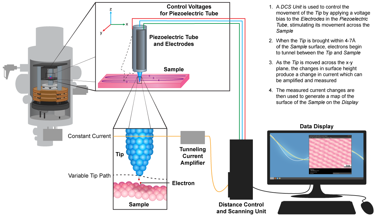
Schematic representation of STM
Inelastic scattering * is the collision of particles, which leads to a change in their state, the formation of new particles, the transformation into others, or the birth of new particles.
A dangling bond * is the unfilled shell of an atom in a molecule or solid.The dangling bonds of silicon atoms have become important components of the study because they are like a kind of atomic quantum dots * , whose electronic state remains isolated inside the forbidden zone * of silicon.
A quantum dot * (or “artificial atom”) is a semiconductor particle. Due to its extremely small size, its optical and electronic properties are very different from those of larger particles.
Forbidden zone * - the range of energy values that an electron cannot have in an ideal crystalline body.Another important feature of dangling bonds is their stability at temperatures of about 500 K (226.85 ° C).
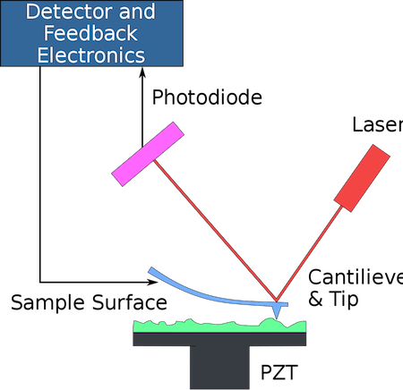
It is clear that hydrogen lithography is fraught with the way to solving the problems of atomic devices, including atomic memory. But for the practical implementation of such devices it is necessary to reach the level of 0% errors, which is extremely difficult. Therefore, the attention of scientists was aimed at increasing atomic accuracy, because the erroneous removal of at least one hydrogen atom can lead to the inoperability of the entire system. This problem could be solved by a new error correction method for hydrogen lithography using a cryogenic atomic-force microscope (AFM) * , when individual dangling bonds were repassivated by means of a microscope needle coated with hydrogen. And again, scientists are faced with a problem. This time it is the speed of the procedure. Despite the high leveling efficiency of lithography errors, the process takes 10 seconds to 1 dangling connection. Plus, delays are added due to the need to use two individual feedbacks and re-cover the needle with hydrogen after each procedure. In other words, the method, though showing excellent results, but requires a lot of time.
AFM * is a microscope that allows you to determine the surface topography with resolution down to atomic.
ASM work pattern
Sample creation details
The sample was created by STM at a temperature of 4.5 K. During the lithography process, controlled voltage pulses were used. And during repassivation, the needle moved in a straight line to the sample using a small bias voltage. For both processes, the control of the STM feedback was suspended, using as a single signal a change in the tunneling current, in which 2 unique signatures were found that contribute to the successful hydrogen repassivation. If these signatures act as control signals, automatic error correction is faster and runs much longer.
Thus, lithography and repassivation, working together, allow us to say with confidence about the possibility of creating a full-fledged atomic-sized storage device. As a demonstration, 2 samples were created: 8 bits and 192 bits.
An important component of the described experiment was also research on chlorine-passivated Cu (100), when a kilobyte of memory is created on surface vacancies without the need for vertical manipulation with atoms. This memory can operate at 77 K (−195.79 ° C) and remain stable for up to 44 hours. This temperature limit was overcome due to the use of structured dangling bonds, which demonstrate high thermal stability even at a temperature of 477 K (203.85 ° C). And the recording density can be increased by 32%, since dangling links can be located extremely close to each other. Also an important feature was the ability at any time (not only when creating a sample) to create or delete broken links, thereby giving the opportunity to overwrite information. However, this statement still remains a theory, since such processes are associated with damage to the microscope needle.
Experimental results
Hydrogen lithography
Incredible accuracy is important in hydrogen lithography. First of all, the position of each hydrogen atom in the selected area must be clearly known for the microscope needle to pass through the sample correctly. The slightest mistake can lead to the fact that the wrong atom will be removed, and this will lead to the inoperability of the sample.
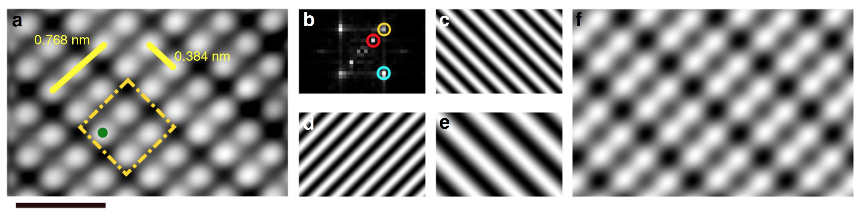
Image number 1
In addition to information about the location of hydrogen atoms, it is also necessary to know the position of other atoms, so that you do not have to repeat the scan each time after performing the lithography procedures.
Image 1a shows a snapshot of the Si (100) -2x1 surface. We can see the distinct periodicity of this surface. It is precisely this system that makes it possible to determine the position of all hydrogen atoms (images 1b-f ) using a Fourier analysis using a single image.
The whole process of Fourier analysis is clearly demonstrated on images from group No. 1. For the detection of hydrogen atoms, images of 10x10 and 40x40 nm 2 were used .
After drawing up a "map" of the surface, the desired pattern is created on the lattice, along which the microscope needle will pass. When the needle reaches the desired point, voltage pulses from 1.8 to 3.0 V are switched on for 20 ms to successfully remove the necessary hydrogen atoms. When the removal is completed, the voltage is turned off.
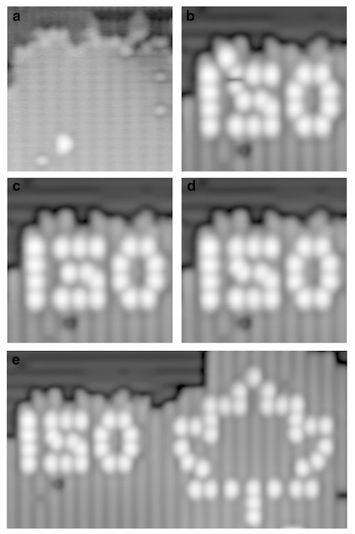
Image number 2
Images 2a , 2b, and 2d show the process of creating dangling bond structures (result on 2e ). And on 2c - hydrogen repassivation to correct errors of lithography.
Since, at a higher temperature, temperature drift * and creep * , leading to errors, begin to occur, the STM operated at a temperature of only 4.5 K. In such conditions, the processes are easy to control, and the STM can be stabilized after a short time.
Temperature drift * - change of electrical parameters under the influence of ambient temperature.
Creep * is a slow process of deformation of a solid due to constant load or mechanical stress. In this case, it is a thermal effect.If it is not possible to do this or the ambient temperature is above 4.5 K, then another method of preventing errors is used. To begin with, a control picture is taken (10x10 nm 2 ) next to the one with which the CMT will work. After a certain time, the lithography process stops and a second snapshot of the treated area is taken. A comparison is made with a control image to determine if there were deviations from a given pattern due to drift or creep. If so, the pattern is adjusted to compensate for flaws.
The researchers checked the results of lithography without such correction and with it. In the first case, the accuracy was only 35%, in the second - 85%, which is a sane result, since hydrogen repassivation can correct the remaining errors.
Hydrogen repassivation
As previously stated, in order to remove errors on the surface of the sample, hydrogen repassivation was performed using silicon needles with a hydrogen atom at the end.
The STM needle approaches the surface of a certain part of the sample and “hooks” the silicon atom, which allows forming the necessary structure of hydrogen repassivation. When the needle is combined with the hydrogen atoms, the differences become visible in the microscope images. A needle prepared for the procedure is placed over a certain broken link at a sample voltage of 1.4 V and a current of 50 pA (picoamper, 1 pA = 10 −12 A). Next, the feedback control is turned off, and the voltage changes by a factor from the range of 100 mV to 1.0 V. During registration of the tunneling current, the microscope needle moves to the sample by 500-800 pm (picometer, 1 pm = 10 −12 m). At the end of the process, the needle returns to its original position, the voltage is restored at 1.4 V, and the feedback control is turned on.
The most surprising thing is that this entire complex and optimized process starts with the push of a single button, runs automatically and takes only 1 second.
We briefly familiarized ourselves with the inherent procedures, therefore we can go on to the most important and interesting.
Atomic memory
So, using hydrogen lithography and hydrogen repassivation, 2 working samples of atomic-sized memory were created.
1 bit was delineated by the four walls of the lattice, setting a buffer of 1 atom between adjacent dangling bonds. This is seen in image 1a .
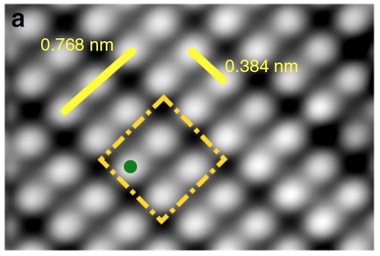
Image 1a
Due to the ideal geometry of the Si (100) -2x1 surface passivated by hydrogen, this arrangement allows to obtain a very high bit density - 1.70 bits / nm 2 .
Sample (a) - Alphabet
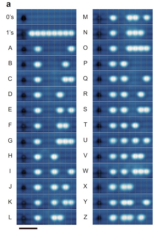
The image above shows 8-bit memory for sequentially encoding the binary ASCII representation of each letter of the English alphabet, overwriting the previous letter each time. It took from 10 to 120 seconds to write 1 letter, depending on the required number of dangling bonds. The most time consuming process in writing letters is hydrogen repassivation, since it is limited by the number of free hydrogen atoms at the tip of the microscope needle. That is, the needle must leave the working area to “replenish the reserves” of hydrogen atoms, and then continue the process. However, this problem, according to researchers, arises only when working with such small objects. If the structure has a large number of dangling bonds, the needle will self-replenish the atoms in the process. Another way to speed up the process is to apply certain materials to create the needle itself. For example, platinum is able to hold about 1000 hydrogen atoms at a time.
Sample (b) - Sound
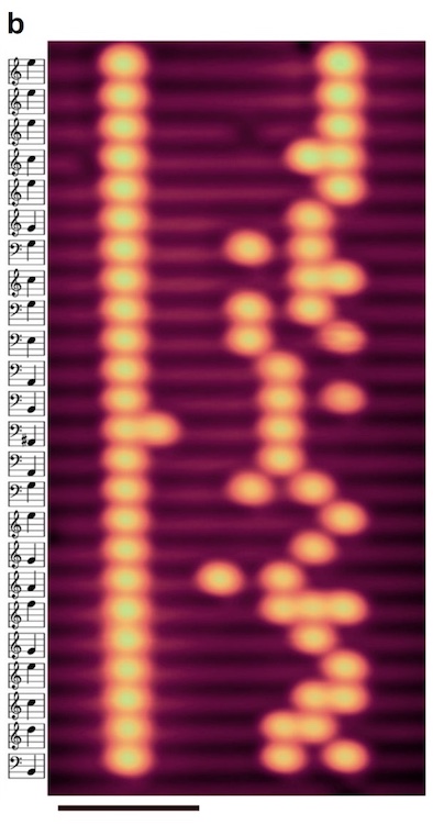
The second sample is larger than the first, it is 192-bit memory with the same bit density, on which a simplified version of the main melody of Mario is recorded. The structure consists of 62 dangling links, and its creation took 250 seconds. This melody could be reproduced both with the help of STM and using the image. You can listen to it by downloading a small video clip , which also shows what a broken link is responsible for which note.
For more detailed acquaintance with the study I strongly recommend the report of scientists, which also describes the methods of measurement and details of the experiments themselves.
Epilogue
This study demonstrated that the creation of a working atomic memory is absolutely real. At the same time, available devices and clear techniques were used. The specific features of hydrogen lithography and repassivation can be adapted for use not only with silicon, but also with other substances, for example germanium or diamond.
Let this technology be in its infancy, but, as we know, all nowadays common technologies were once in a similar situation. The implementation of any technology or device requires not only the practical use of scientific knowledge, perseverance, time, a large number of experiences, but also a little imagination. No wonder Mr. Feynman in the video said:
I do not want to take this seriously (regarding science). I think we should have fun (have fun) and stop worrying.Thank you for staying with us. Do you like our articles? Want to see more interesting materials? Support us by placing an order or recommending to friends, 30% discount for Habr users on a unique analogue of the entry-level servers that we invented for you: The whole truth about VPS (KVM) E5-2650 v4 (6 Cores) 10GB DDR4 240GB SSD 1Gbps from $ 20 or how to share the server? (Options are available with RAID1 and RAID10, up to 24 cores and up to 40GB DDR4).
Dell R730xd 2 times cheaper? Only we have 2 x Intel Dodeca-Core Xeon E5-2650v4 128GB DDR4 6x480GB SSD 1Gbps 100 TV from $ 249 in the Netherlands and the USA! Read about How to build an infrastructure building. class c using servers Dell R730xd E5-2650 v4 worth 9000 euros for a penny?
Source: https://habr.com/ru/post/418123/
All Articles