iMX6ULL. Transition to processor modules

Good day!
Attention, a lot of text and photos. There are many variations of single board PCs with shield or all-in-one solutions on the market. Some are sharpened for specific tasks, for example, data collection and display, others are universal and include all sorts of interfaces for all occasions. Significant differences are also observed in the configuration, types of fastening, connectors, form factor, etc. Why develop your device, you ask, if you can choose already commercially available? Several years ago, turning the board on the IMX6Q - “BD-SL-i.MX6” from Freescale (read NXP) - had the idea to make a module that ...
1. Covered our needs for prototyping boards on the IMX6. At that time there were already several projects implemented on this chip. It is worth explaining that having your module and developing a motherboard for a specific project, you can quickly test the entire periphery, “pick up” software, make changes and transfer everything to the same 8 layers that are necessary for IMX6Q (the line of these chips is not limited to quad-core In addition to QUAD, there is also a DUAL and SOLO option - all “pin-one-pin”, which gives ample opportunities to implement devices of different functionalities based on one “board”). Let me remind you that the motherboard can be 4-ply and even 2-ply, which significantly speeds up the time of its production and reduces costs.
2. Use the module as a component and give the customer a choice: transfer all to one board or use as is. In fairness, I will say that the use of purchased modules for commercial projects is not being considered. First, you cannot find a module that would suit everyone (either there are many connectors, or few, or there are no mounting holes, or the board is large, etc., in general, who has been looking for his needs, he will understand), but -second, its development is always safer. You can shower me with tomatoes, but I trust only myself.
3. Give the customer the opportunity to develop their device based on our module. Yes - it also turned out to be in demand, but not the one described above (about the difficulty of selecting a module), but the fact that it is Russian development and production plays a big role. Apparently, the word "import substitution" has greatly influenced our industry and development, including.
')
IMX6 start
Briefly about the main thing, but it will not be the essence of the article. Our first module on the IMX6Q is used and is now in development, has dimensions of 50x75mm. OS Linux and Android.

Fig. 1. Module on IMX6Q
I will not list its interfaces, advantages and disadvantages. It displays almost everything that has a chip, and this is quite enough for the implementation of many projects. On board are eMMC, interface connectors, Ethernet gigabit physics and power. A brief digression finished, now the essence.
What we came to
The IMX6 line does not end on the above chips. The IMX7, IMX8 in various versions has already appeared, but we were interested in a weaker version in smaller dimensions, trimmed in functionality - this is the IMX6UL / IMX6ULL (they are also pin-to-pin among themselves). We paid attention to it for a reason, and because several tasks appeared at once connected with voice over Ethernet using the SIP protocol, as well as the need to develop devices in small dimensions and without the possibility of heat removal. The IMX6UL has a pretty good onboard peripheral kit:
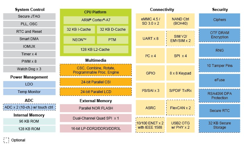
Fig. 2. IMX6UL Block Diagram
Those who have little pictures, can get on the NXP website and look at the details of the chip line. One of the advantages of using this processor is its case. The pitch of its contacts is 0.8mm, and the contact pad is 0.356mm (BGA), which means that the board can be made on 4 layers (which, in principle, is done in the NXP reference card on this chip). We use version 14x14mm (there is also a 9x9mm with 0.5mm increments).
Why exactly NXP, and not Broadcom, ST, Ali or some other processor giant? In fact, it’s all about chip availability, tech support and cross-platform. Having made a module on IMX6Q, we relatively simply ported software to IMX6UL / IMX6ULL. Pin-to-Pin chipsets, so by debugging UL software, you can switch to a cheaper ULL. The second is low power consumption and, as a consequence, low heat. I deliberately do not cite the technical parameters of the processors, so there is a lot of “water” in the article, and this information is publicly available.
One of the interesting projects implemented on the IMX6UL is a voice over Ethernet device - a SIP phone, and in fact a communication device.
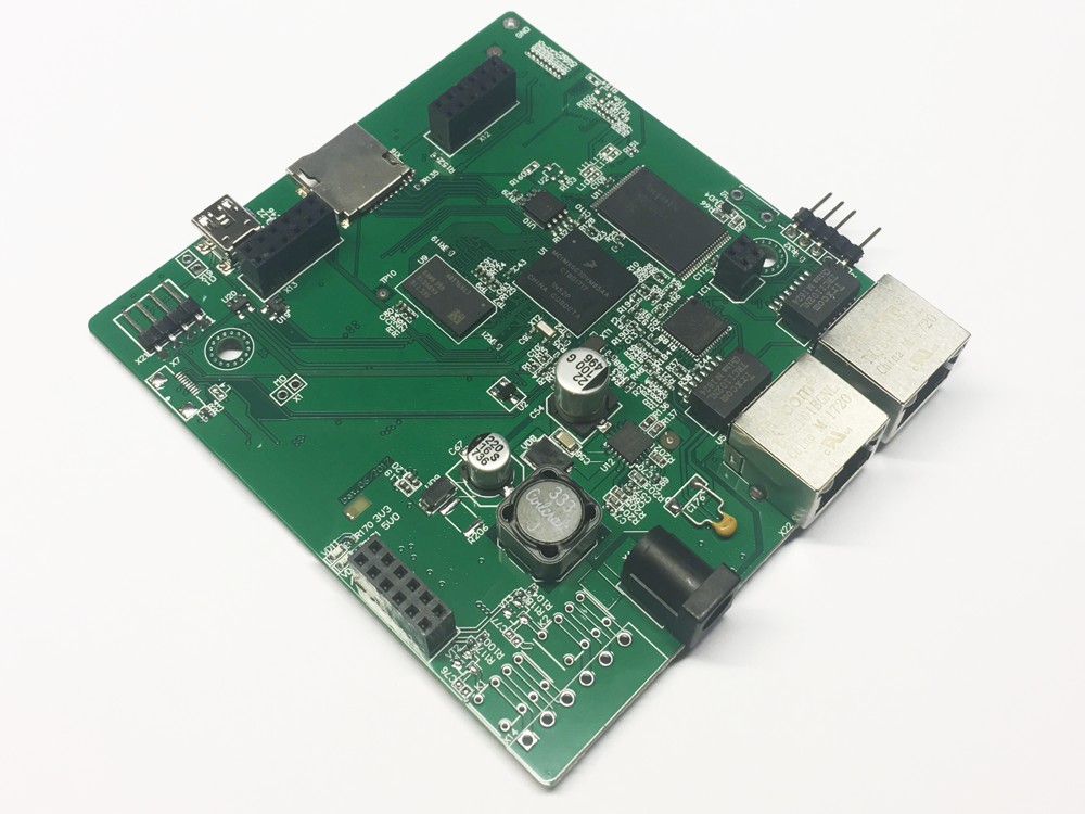
Fig. 3. SIP phone.
The main thing
The heart of the project is IMX6, on which the OS “rotates” with the SIP client installed. Before booting Linux, the u-boot (boot loader) is loaded from a separate SPI Flash. The separation of the bootloader and the main firmware was not made by chance (unlike the reference), but in order to make the device durable with an unexpected power off. If you start talking about ubifs and the read-only partition on NAND, then I’ll be very upset. Practice has shown that even the best NAND chips have the right to die and do so quite unexpectedly. For communication with the outside World there is an RMII interface, and an Ethernet switch LAN9303 - 10/100 is installed on the board (this IMX does not support gigabits) and two ports were needed. IMX6UL has two RMII ports with routing, but there was a need for precisely two independent interfaces in the form of a hub.
NAND is used to store the firmware and files (We stopped at Samsung K9F1G08U0D in the TSOP48 package. We do not begin to spit and do not close the article, since the memory in such a form factor is very cheap in small batches compared to BGA63). One DDR3 memory chip is K4B4G1646D, codec ADAU1761. The codec is worth more details. Prior to this, several projects used SGTL5000, but with ADAU, life has become much more fun. You can write a separate article about him, but I will try to summarize its essence in my project. Not only does the chip have 6 analog inputs, 7 outputs and, of course, the I2S interface, also Analog Devices together with the codec released specialized software for it to write firmware for the built-in DSP. Who cares, and who does not know you can read the info about what DSP is and what it is eaten with.
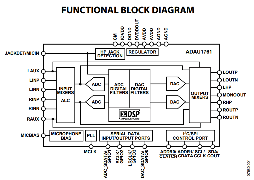
Fig. 4. ADAU1761 Block Diagram
At the time of writing the software, the first thing programmers played was with all sorts of functions of distortion, echo suppression, filtering and sound mixing. At the hearing is very impressive, I tell you. The interface is very user-friendly, many settings, filters, transformations, the possibility of redirection of sound, etc.

Fig. 5. SigmaStudio from Analog Devices
The project involves 4 channels (input / output), as there are built-in stereo speakers and microphones, as well as connectors for connecting external ones.
The board (in Fig. 3) joins the top of the peripheral board, just with the codec, the matrix keyboard scanner, etc., did not write about it.
One of the RJ45 connectors is used to power over PoE; the Si3402 chip from Silicon Laboratories is used as a Powered Device (PD). The switching circuit was used almost standard without galvanic isolation with an output of 12V (the voltage is adjusted by resistors). A little distracted, who is interested in the topic of PoE + with galvanic isolation, there is a very good chip from TI - LM5072MH-80. Excellent proven in several projects.
Secondary power supplies are implemented on DC / DC ST1S10PHR - not the cheapest, not the highest frequency, but they work fine and are available by carriages. In general, we have a whole DC / DC zoo and LDO for different needs, but when quality is important, choose well-known manufacturers.
The board also has USBHOST, USBOTG and SD card. Through USB and SD, you can roll / update the firmware. There is also a network update, but this already applies to the software and to the web interface.
Little tracing
You can endlessly post gerbera and pieces of trace boards, but I will not do this, and will only touch on the main and critical moments. The order of card layers is standard:
- TOP - signal with land polygon
- GND - land polygons
- POWER - food polygons
- BOTTOM - Signal with land plot
1. DDR3. It is necessary to be careful with self-allocation of memory, so I did not do this, but took the reference as an example. Only two layers are used for tracing (top and bot), the other two layers are not used. Through holes 0.203 / 0.406mm, line thickness 0.114mm. I changed only the ground lines under the processor and made them a bit thicker - up to 0.3mm. On the GND layer, we got a good earth, in which I had to carry out an RGB interface, which is not entirely correct, but I just did not see the other option with my number of interfaces on the board.

Fig. 6. Tracing memory
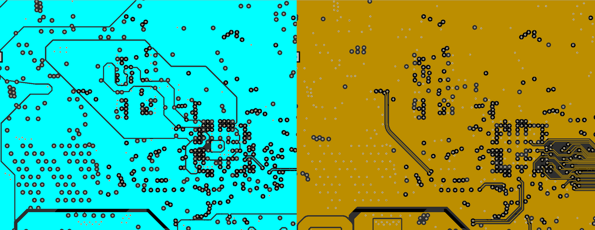
Fig. 7. Polygons of food and land
When distributing the board, you need to spend more time on the land and food landfills. It is much easier to develop 4-layer boards with the same schematics, there is a gap in the trace of signal conductors and there are always two layers for good power, which can also be competently used under non-critical data lines. The main power range is almost always I do 3.3V, the rest is inside it. All high-voltage polygons are made with large gaps to eliminate interference.
2. PoE, as I wrote earlier, is implemented on a Si3402 microcircuit. It is divorced strictly on four layers of the board with large gaps from the main polygons. I think it will also start on two layers, but no one guarantees the quality. When designing power units, I usually follow the evaluation board for microcircuits, and when testing, I check the waveforms given in the documentation. If it is impossible to do both in the reference, due to the size or configuration of the board, then you have to be guided only by experience and common sense.
In the power layer for PoE, there is a 12V polygon. The remaining layers are used for signals and polygons of the earth PoE - GND_EXT. All polygons are strictly under each other without “overlaps” on adjacent polygons in other layers. The indent between the PoE polygons and the main order is 1mm. When developing a PoE with galvanic isolation, I usually additionally make a cutout cutter (in the manufacture of boards) under the transformer and feedback optocouplers.
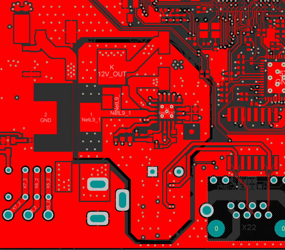
Fig. 9. PoE. TOP.
3. Peripherals. I had to do the layout of the board on the M3616 chip of the ALi Corporation, it has only 292 balls, but look at how well the processor is designed to make the board easier to trace. How clearly all the interfaces come out in the right order. Attention, the board is divorced on two layers, and the RAM is completely in one.
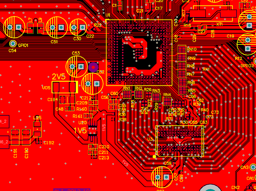
Fig. 10. Polygons of food and land
On IMX6UL / IMX6ULL it was necessary to tinker with interfaces. In fig. 6. You can see how tightly the conductors go and there is not enough space for vias, but you need to remove them from the 5th row of balls. Here the main thing is to observe the impedance in differential pairs (for example, USB) and not to overdo it with vias, as this will damage the land and power polygons.
And yet the module
What not to do, but still get a module. When the number of projects on IMX6UL / IMX6ULL exceeded expectations, and the main functionality was written, it was decided to switch to a modular system, as last time, and also to make it elegant.

Fig. 11. Module mx6ull-m02c on IMX6UL / IMX6ULL
Why elegant?
- The module is made in the form of "on the board" and has no interface connectors, allows its use as a "chip".
- Onboard, it only has everything you need: a chip, DDR3, NAND, SPI, Ethernet physics, one 1.35V feeder (which allows you to supply only one 3.3V voltage to the module), quartz and passive.
- One-sided installation. Not every modular solution can boast a lack of components on the bottom. This gives several advantages at once: heat removal to the motherboard, the possibility of tracing under the module (since there is no cutout on the board for protruding components) and cheaper production of the modules themselves (minus the stencil, board flip during installation, etc.).
- Pads on the perimeter of the board. There are no signal soldering points under the module.
- The dimensions of the module are only 45x36mm.
- Somehow I will talk about one of the devices developed on this module, but for now a photo of the motherboard for debugging and writing software.
Fig. 12. Module IMX6UL / IMX6ULL on board
The board is double layered and has interface connectors necessary for starting and running. On such boards, we conduct internal testing for cooling and heating during operation, check the stability of the work under load, and debug the software.
Conclusion
What exactly does a modular system, when developing devices?
- With the existing module, the development time of the board with external interfaces takes only a few days (provided that all interfaces are clear and used earlier in the development).
- Printed circuit boards are an order of magnitude cheaper, since in most cases you can make a double layer, or a 4-layer board with a lower class.
- The speed of getting the motherboard is much higher, because you do not need to solder components related to the module.
- The transition from the layout to the release version is faster and more painless (if you decide to make a single-board solution).
Of course, all projects are different and sometimes the peripheral circuitry is an order of magnitude more complicated than the processor itself, but debugging of individual modules is always easier, especially if the development of a single project is carried out by several engineers.
Within the framework of one article it is very difficult to write everything you want. Describing even one project takes a lot of letters, but I want to touch on several projects, share impressions about various peripherals, chips used, interface tracing features, etc. But the main thing is to stop in time.
PS: link to github.com/trotill/adk_yocto source
Thanks for attention!
Source: https://habr.com/ru/post/411151/
All Articles