My little relays: Brainfuck computer is reality
Exactly one year has passed since the last publication, and I thought that April 1 is a great day for the annual digest of my three crazy computer projects. At that time, the project existed only on paper, but now it has definitely become a reality.
Rolling up ringing relay blocks, the fastest in the world of calculations on the relay (but this is not accurate), wrap-up installation, vacuum indicators and flashing LEDs.
History reference

Figure 1: Battered by life and me personally, Wojciechowski’s volume “Radio-electronic toys”, 1979
A long time ago, when everything was big around, and I was small (the year since in 2002), my father presented me with a book by Wojciechowski, Radio Electronic Toys. At that time I didn’t have a computer, but I didn’t even hear about the Internet, and the book familiar to many turned out to be just a storehouse of entertaining electronic devices. Among them was the description of the electronic computer and the scheme of a simple model on telephone relays. This model, being a second-year university in 2008, I collected for a report on the history of computers.
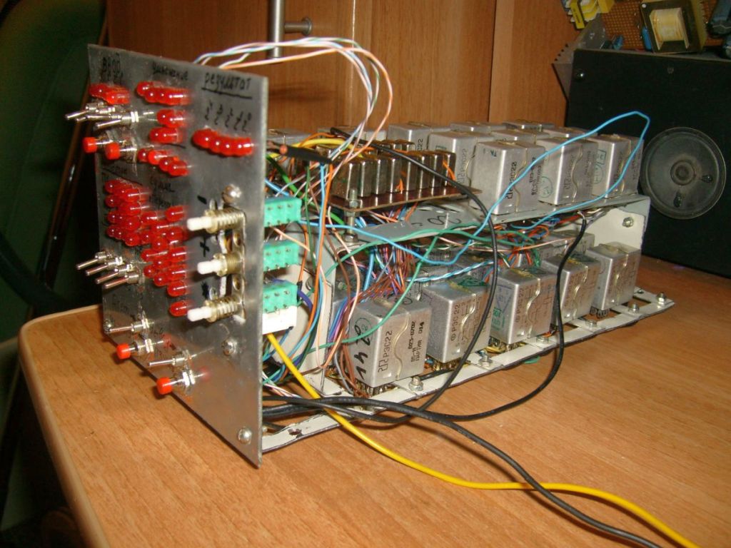
Figure 2: RCWM - 4-bit ALU
At that time, I was already studying the Internet, and being aware of the existence of Harry Porter’s relay computer , relay computer No.2 and Zuzu relay computer , I was thinking about building my own unit.
For those who have little idea what others have there, I suggest viewing my own video review of home-made relay computers. For the year it is just a bit old, but it has not ceased to be less interesting:
In the same 2008, in the classroom on the theoretical foundations of electrical engineering, I decided on the main component - the reed switch. In one of the laboratories, I was surprised to see on the oscillogram how the small RES55 worked at a frequency of 50 Hz. This made an indelible impression on me and I began to accumulate reed relays.
10 years have passed ...
And a decade later, the project is moving towards release with great speed. Everything moved from the dead point in November 2016, when the current architecture was born. Unfortunately, I decided to make all the printed circuit boards by myself ... as a result, a whole square meter of double-sided PCB turned into a black hole and sucked into several hundred man-hours of free time, which is about half a year for an employee. From April to November 2k17, almost nothing happened.
Infographics
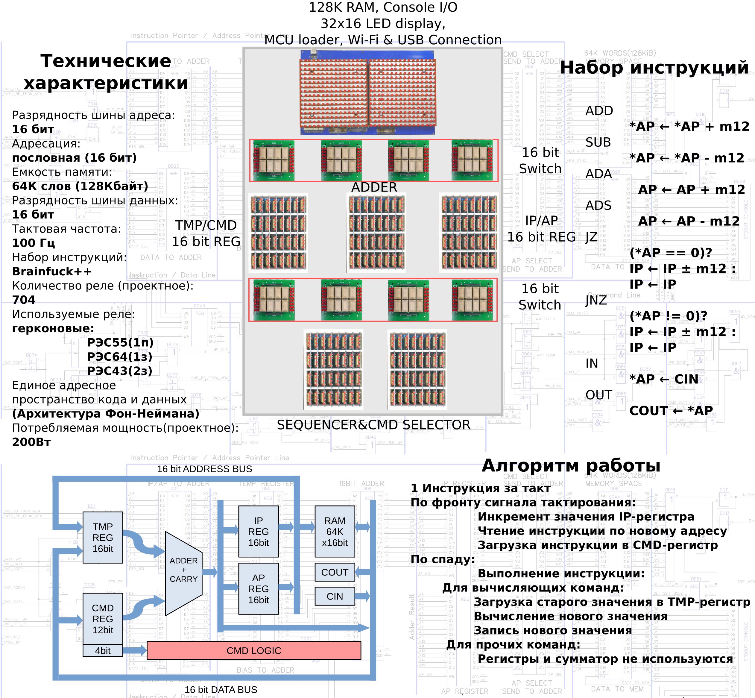
The architecture of the machine corresponds to the Turing machine. There is a tape with data - 64 kiloslova RAM (16 bit word). RAM - cache chips from some kind of mate. motherboards for Intel Pentium. For authenticity - go to ... the “Authenticity” section. Microcircuit RAM is used in most homemade relay computers known to me.
The central element is a 16-bit parallel-transfer adder. He is responsible for calculating the number of the next instruction, and works with the data and a pointer to it.
At the inputs of the adder hang 16-bit temporary register and 12-bit command register. 12 bits are also fed to the upper 4 bits of the adder, which gives a “full” 16 bits. It is important that the adder works correctly with the addition and subtraction of a 12-bit number.
The disadvantage is obvious - at a time we can jump only 2 ^ 12 instructions backward, or forward, or change the pointer or data to this value. The first is to take into account when writing programs, for the second one you can always repeat the procedure.
Subtraction is in the additional code. Parallel transfer provides a constant computation delay — only 3 series-standing relays. This is not more than 2ms.
The IP register and the AP register, as well as the RAM input, are connected to the output of the adder via latches.
Calculations
Basic operations - exactly two pieces. In one case, we work with calculating a new pointer value, in the other - a new data value.
Each rising edge starts the calculation of the new instruction number. IP ++ is essentially done. After the calculation, the IP is fed to the address input of the memory card and, via the data bus, the instruction enters the command register. The high 4 bits determine the future instruction, the low 12 most likely do not equal zero, and in the future the adder will change the number in the time register by exactly this value.
Each falling front begins the operation.
For operations with AP and IP registers, the sequence of actions is as follows:
- Through the address bus, the contents of the IP (AP) register are copied into a temporary register;
- Temporary and team registers are fed to the input of the adder. After 2ms at the output of the adder will be ready to answer.
- The response is recorded in the IP or AP register.
There are some features. For the AP + BIAS and AP-BIAS commands, everything is exactly the same, for conditional commands, when for example IP = (* AP == 0?) IP + 1 is done: IP + -BIAS, we still need to unload the current value of the data cell and remove information from a null detector.
For AP + BIAS and AP-BIAS operations, the sequence is slightly different.
- Via the data bus, the current value of the memory cell is written to the temporary register.
- Temporary and team registers are fed to the input of the adder. After 2ms at the output of the adder will be ready to answer.
- AP register continues to be fed to the input of the memory board. The answer from the adder is written directly into memory.
Calculations always happen in 16-bit mode. But the zero conditional flag is defined as:
Z = ((16bit?) *AP : (*AP) & 0x00FF == 0) ; Design
Since last time, nothing has changed.
Module
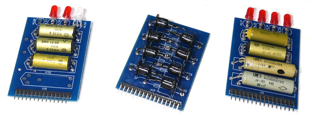
Figure 3: Computer module. Left-to-right: D-flip-flop module, diode module, 2AND / 2XOR module
At the base - a small module 40x64mm. Each module is a printed circuit board with 4 relays on which a simple logic operation is implemented. There is a connector for 16 pins (there are modules for 12 and 14 pins) and up to 4 LEDs. All sizes are strictly fixed.

Figure 4: Modules in the build process
For example:
- Module 2AND / 2XOR - 2 independent logical operations - 2AND and 2XOR. 32 pieces are used in the block adder, two modules per bit. At first, all 4 LEDs were soldered, but the module circuitry is such that two relays on each module are connected in parallel, and to reduce the power consumption by the unit, half of the LEDs were removed.
- D-flip-flop module - 64 pieces go to two register blocks. Of these, 60 are triggers without the Enable signal.
- The diode module is just 8 diodes on the board for implementing a multi-input diode OR. Dirty hack, but it allows saving both on the relay (I now have about 400 relays in reserve) and on time - as compared to the relay, the signal is transmitted to the output of such a logic element instantly.
- Module 2 & - This is the base brick. In fact - 4 relays with a switch contact for the implementation of absolutely any logic circuit. Will go to logic blocks in an unknown quantity.
- Universal 2AND / 2OR which is made so that it allows you to implement almost any logical function - 4AND, 4OR, 4AND-NOT, 4OR-NOT and so on. Also go to the block of logic in an unknown quantity.
As I said, after wasting a lot of time on making home-made printed circuit boards, I went nuts and ordered a complete set of boards from the Chinese. In the first week I collected the first modules. A month later, all the modules for the adder unit were ready.
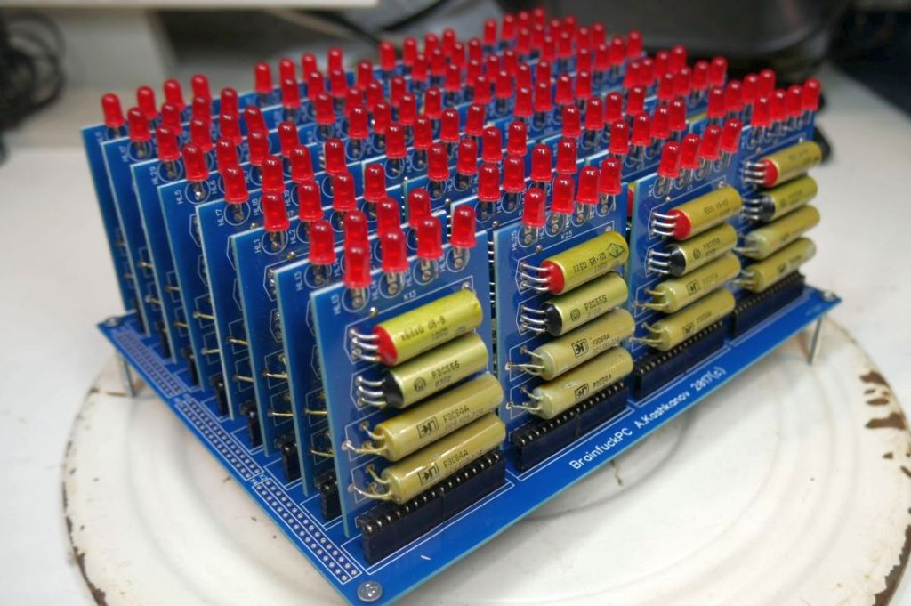
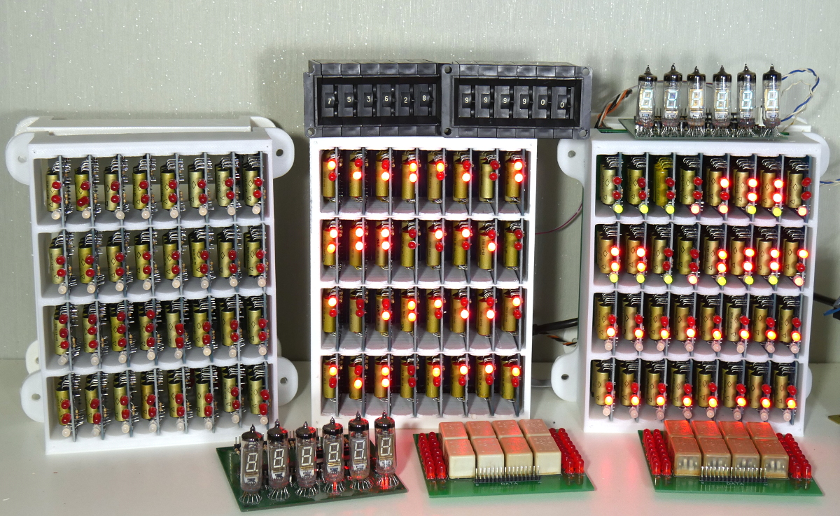
Figure 5: Adder Block
Block
32 modules of 8 modules in 4 rows are combined into a functional unit. Total blocks 5 (in the worst case - 6):
- Adder block - a 16-bit full adder. Two 16-bit inputs for numbers, 1 zero-bit carry line, Two outputs. On one - the operation of summation, on the other - XOR between the inputs. It can be used as an independent operation.
- IP / AP register block - Two independent 16-bit registers without the Enable signal. The pins Q and ~ Q are used directly and are fed through the latch where it should. It was possible to solder 4 relays, but for the sake of economy, the relay functionality was moved to external latches.
- Block registers TMP / CMD - There are three registers. One - 16-bit - temporary register. Exactly the same as IP or AP. The second one is 12-bit, its output is connected to the input of the adder via a latch. The third is 4-bit, with built-in Enable signal. It is used to store the current instruction.
- Logic blocks - 2 pieces. Or three. The scheme is still unknown. Preliminary calculations show that 64 modules will be enough (GOTO: Memory Board).
At the base of each block is a base board - 200x150 mm, without wiring. All that is on it is 32 connectors and square pins sticking out from below for mounting by wrapping.
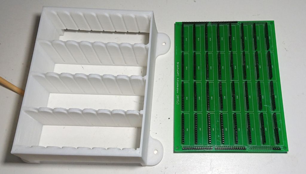
Figure 6: Baseplate and basket
Just because the modules sticking in the connector are not reliable. They will dangle back and forth, shift from shaking and in every way reduce the reliability of the structure. To fix them, I drew and printed out special baskets with grooves. They certainly will not get anywhere modules - they survived the train ride to Moscow and back without any problems.
The basket could be drawn and easier - a layer of 0.32 mm print it a little more than 10 hours. Three baskets printed with PLA-plastic, two more - HIPS. The latter, due to the lack of a casing in my printer, noticeably jars upon printing.
You may notice that the block adder has no ears for mounting. The basket for it was printed the very first. Then I either finish these ears, or print a new basket.
Figure 7: Adder block and logic block.
Wrap installation
On the baseboard we are waiting for 600 conclusions, which need to be interconnected. The blessing that you need to connect is not just everything, but only almost everything. On the other hand, it does not make it any easier.
We take in hands a special tool, a coil of wire and a leg behind the leg we wind the connection diagram.
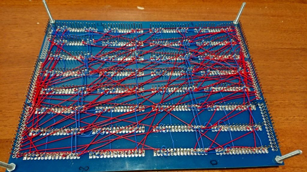
Figure 8: Mounting by wrapping an adder block
This is just the beginning of work. Well, as a start. At first there was a quiet horror - the wires lay haphazardly, some jumpers were long, others were too long ... Having learned to do a little better than it was, I took off most of the jumpers and twisted it all over again - I began to tighten the jumpers with a string. So the wires do not hang out, and the result looks much better. I tried to put so that the wires do not put pressure on the corners of not their pins. As a result - not a single circuit. From the first attempt there were only earthen lines.
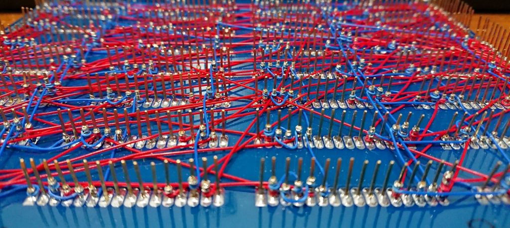
Figure 9: Mounting by wrapping a block of adder. Final result
At the moment, it’s not exactly straightforward, but for the first board it’s a very good result, I think. Until now, I have not learned to put the wire coil to the coil, or the curve tool, or the hand ...
At comrade. UA3MQJ there is a detailed article on this method of installation.
In addition to the block adder, a block of registers is needed. Rather, two blocks of registers. Another couple of months - and another 64 modules were assembled and tested. It remains to wind the base board.
How it was.
Indicator modules
Figure 10: Indicator Module
The current state of the processor registers must be displayed on something and I decided that the vacuum indicators would be just right. On the 100x100mm board (for 10 pieces of this size, you can order from the Chinese for $ 5) there are 6 IV-6 indicators, K155TM8 triggers and a microcontroller. The indication here is dynamic.
There is also a 16-bit input for direct reading of the state of the register and a UART port for receiving commands from the memory card.
Now the firmware can read the state of the 16-bit port and output it in the HEX-format to the indicator. I need a total of 4 of these modules. Three will display the current status of the registers - IP, AP and CMD register in order to have a more convenient visualization of the current stored values. Fourth - will show the total number of instructions executed.
Latch
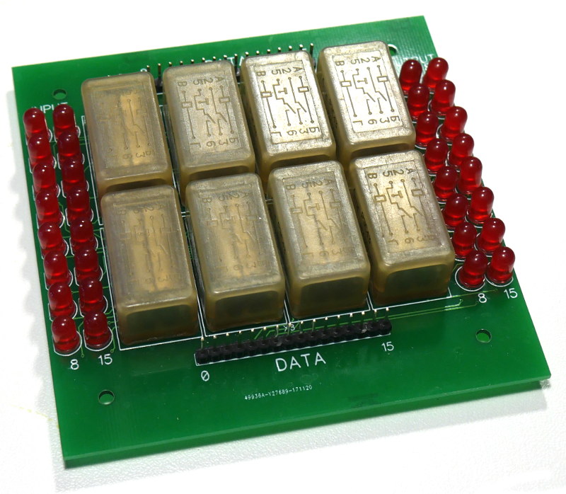
Figure 11: Latch Module
The latch module consists of 8 relays RES43. Inside - two make contact. On the left and on the right are LEDs displaying the current status of the input and output.
The size of the latch - 100x100mm. Required quantity - 8 pieces. Two are ready, it remains to collect six more.
Memory board
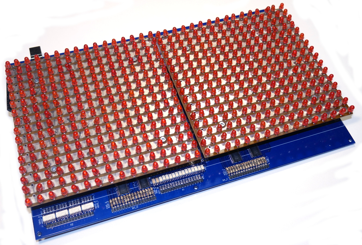
Figure 12: Memory Board. General form
The most huge block containing, first of all, two 64 KB static RAM chips and matching circuits for address inputs and a data port. The board is a microcontroller ATmega1280. He has two vital tasks:
- Download the program and the initial data in the RAM. The compiled binary should be placed in memory. To do this, it will be possible to connect to the memory card via UART or telnet (via Wi-Fi) and download the executable file. MK will read the header and decompose the sections of code and data in the RAM. I am completely lazy to do this with the help of toggle switches and buttons - a brainfuck program that knows how to do something harder HelloWorld contains thousands of instructions. There are a few trump cards in the stash on this, but about them another time.
- Implements commands to read data from the console and write to it. Yes, the instructions "." And "," are implemented using the MK. Rather, the relay logic informs the MC that it is now necessary to transfer the status of the data bus to the console, or, alternatively, output the value from the console to the data bus. In fact, the MC works as a parallel interface converter to the UART. Yes, it is quite possible to perform on any specials. microchip and I'll think about it.
Still not decided what to do with the 16-bit mode. Of course, most programs are written under the 8-bit brainfuck and everything is simple - we read and write the low byte. And in 16-bit mode, what to do? Display the entire word or also only the low byte?
In addition to the main ones, the MK has a number of side problems, which, in principle, can be done without, but they are aimed at the convenience of using the machine:
- MK is responsible for outputting a small area of memory to the LED matrix of 32x16 pixels. He does this while the address bus and the data bus are not occupied by the main logic. Here I am not sure that for MK in general there will be time on the bus, so the question requires verification. But in the program header there will be a starting address for displaying and I will try to make it work. Indication - dynamic. In one clock cycle, two data columns are displayed at once.
- When activating a protected memory mode flag in a binary, in the case of an attempt to execute a data section or writing to a memory section, the MC generates an exception “Segmentation Fault”. So we can make sure that the program does not go anywhere. Reading the memory section is not prohibited.
- When activating the code control flag, the MC activates the simulator and will follow the same instructions as the computer, comparing the expected and received results. If the result is different, the “Machine Error” exception will work. This will mean that an error has occurred in the calculations and possibly one module has begun to fail. Either we are too pulled up the clock frequency and the relay no longer has time to calculate. Just with the help of this functional, I will try to squeeze the maximum out of the car - something will have to control the correctness of work during this period.
There is also a temporary, but still vital, function of the memory board - emulation of a logic block until it is there. On the memory board there are input and output lines and we can send the necessary signals to the blocks. So, connecting all the control lines to the memory board and writing a program, issuing the necessary sequence of commands will turn out as soon as possible:
- run the first programs for execution;
- debug the logic circuitry algorithms and circuitry, which will increase the chances for its error-free assembly and operation later.
Then, collecting the necessary modules of logic blocks, all functions will be gradually transferred "to hardware". When the MC is no longer responsible for the logic - the project will be considered completed.
Authenticity
The project was not originally conceived as a purely relay, without the use of transistors and microchips. On the one hand, the computer turns out to be hybrid and loses in radiation resistance, on the other hand, most relay computers have the same ailment. In the final version of the machine, the memory chip and the microcontroller will be used. Ferrite memory will be used in another, already “Silicon-Free” project.
To compensate for the effect of the necanon, I got an electronic typewriter “Robotron S6130”
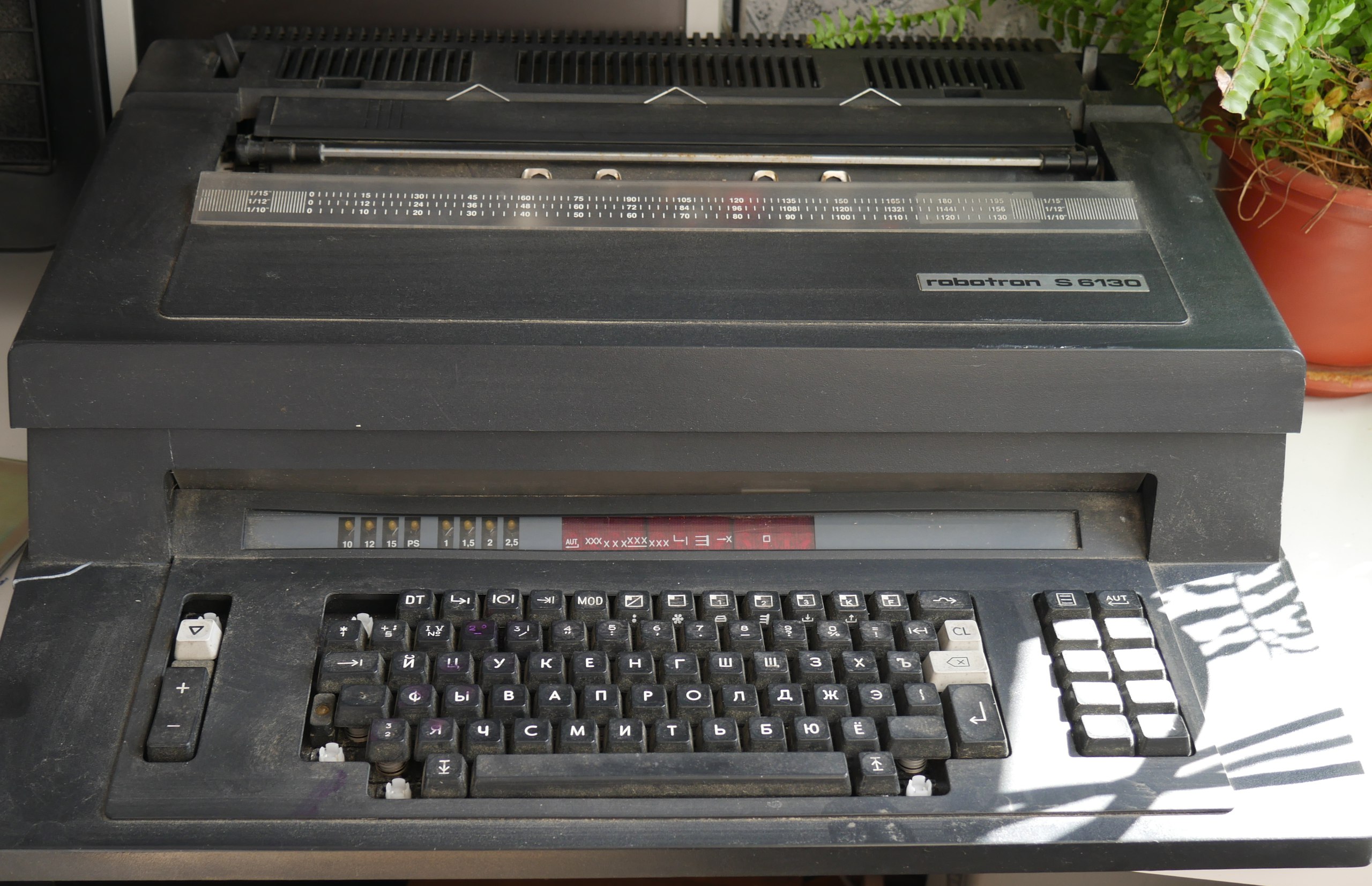
Figure 13: Chamomile type electronic typewriter.
Unfortunately, I got the machine in a state of shabby life. She was used for a long time in accounting, but in the end she was left to die in splendid isolation.
I recommend to view a unique review of this monster.
The mechanics were in good condition, but the processor board, on which a pair of D-0.25 NiCd batteries stood, was very powerful. They safely leaked and strongly filled with electrolyte all around.
I want to restore it and use it as an I / O terminal for a computer. However, in addition to the malfunction of the electronic part, the machine has a Russian chamomile (a disk with letters) and Russian keys. The second is solved by stickers, the first is to be looked for and here I have no luck yet. About the fact that a ribbon cartridge is required, I generally keep quiet. At least I have paper for it ..
If it is decided electronically that it is irretrievably lost, then I will try to find a donor, or I will develop a new electronic filling. To make a management board for a handful of footsteps is not the most difficult task. It will be harder to translate from the German manual and understand the TK. Of course, this car deserves a separate article on the results of the revival. Against her, for now, is the priority of the work being done.
Tests
All those who read up to this place are waiting for a reward in the form of crackling and buzzing relay blocks.
To begin with, let's try to send a square wave to the input of the relay, through a transistor cascade:
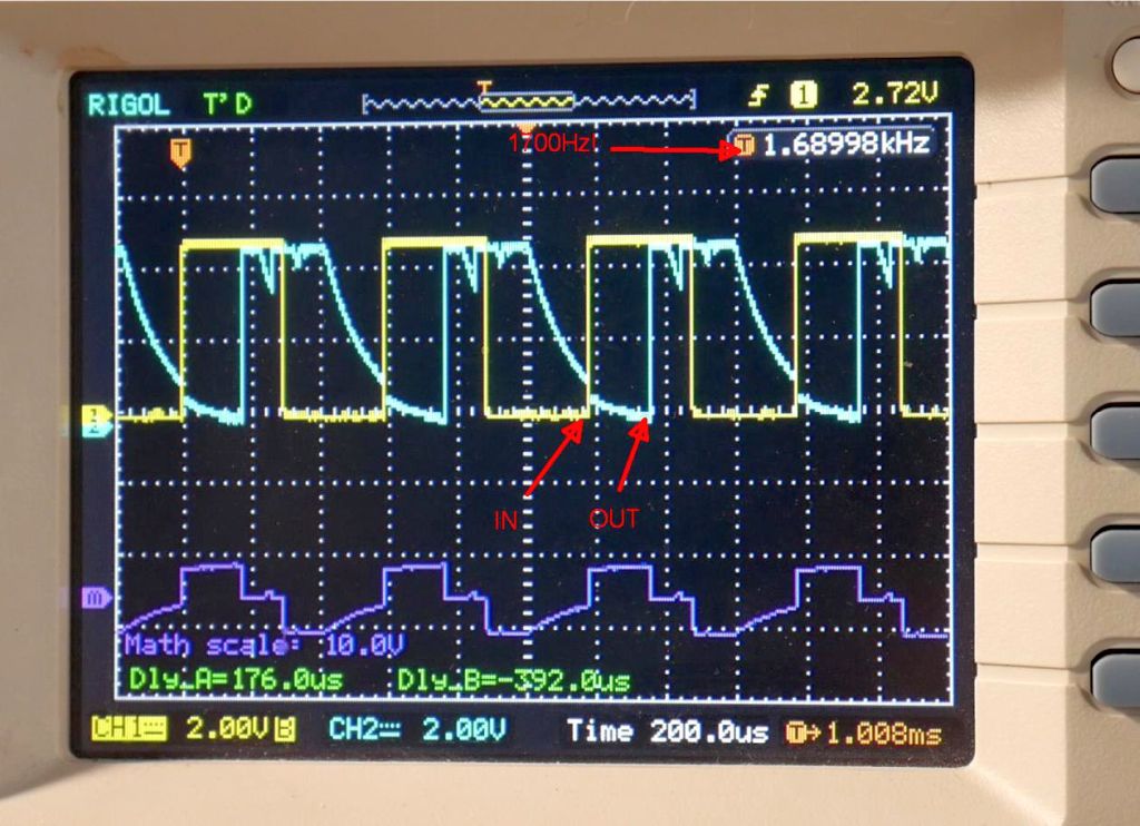
Figure 14: High-speed testing of reed relays RES55. Yellow signal - on the coil, blue - on the contacts
Since the oscilloscope input has a certain capacity and after the relay contact opens, it remains in the air and self-discharge begins, we see the opposite exponent. At a frequency of 1.7 kHz! For the relay! For one small reed switch! Conventional stall at 20Hz or slightly higher. At a nominal frequency of 100 Hz, the rising and falling fronts are approximately 600 µs each. Here they are so small (200µs), since the coil still has energy from the previous one at the time of the next switching on.
We energize the blocks, cut the switches from the Soviet gauges to the inputs.
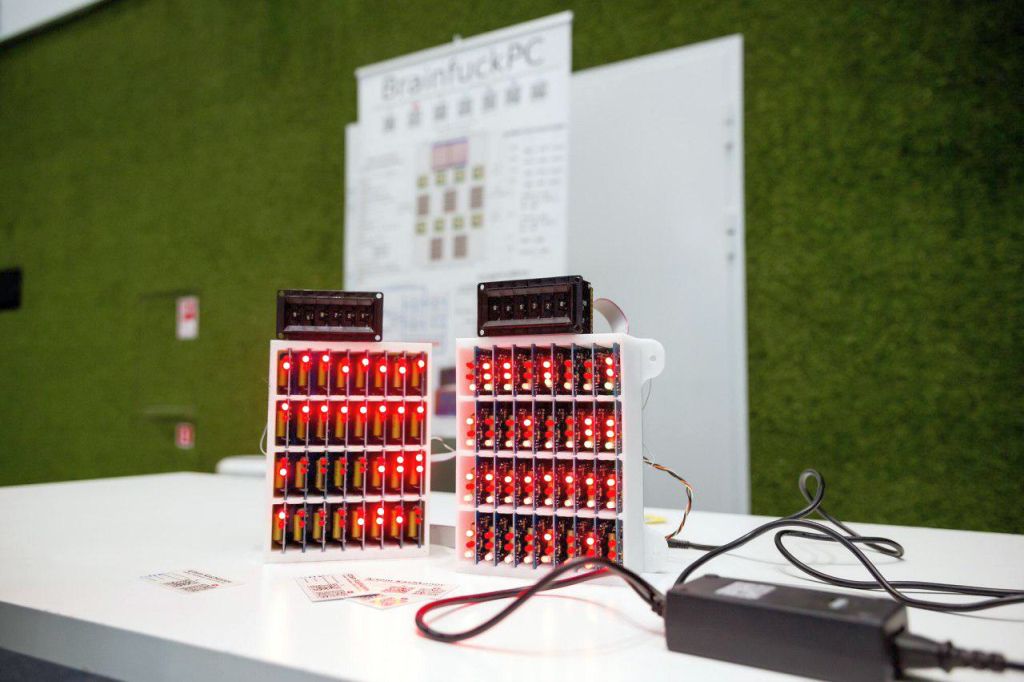
Figure 15: Adder block and register block in operation
It counts! Cool.
So it looked from the scene. At first I wanted to remake the switches under 16-bit. Connect the indicators and the input and output, but ... I could not resist.
Well, since everything works, and the relay turned out to be capable of insane speeds, we submit a square wave to the transfer line:
And we cut 500Hz. Adder copes, although the sound of this can not be said. In fact, the sound is clear, but the condenser microphone considers otherwise. As far as I know, this is the fastest relay adder in the world.
To be continued
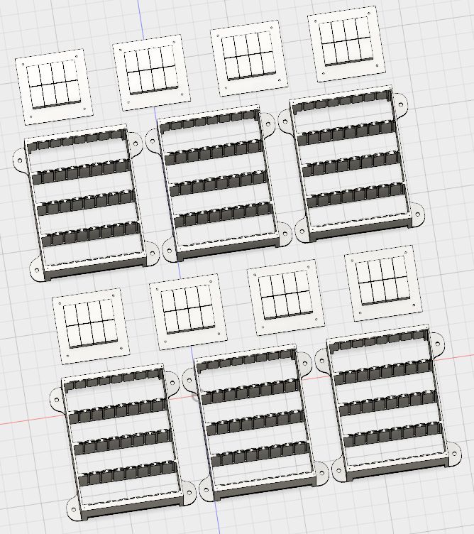
Figure 16: Computer Frame Design
The missing six pieces of the latches are gradually collected and the frame of the future car begins to be projected. There are six blocks in the drawing in case the 64 logic modules are not enough. And if that's enough - the space below the lower central unit will remain empty.
At the same time, I am writing a firmware for the memory board, so that it can replace the logic block that is still missing. In summer, the computer will be able to execute its first program.
Three computers ???
Yes, three. The first is the current BrainfuckPC. The second is a pneumonic computer, codenamed FluidicPC .
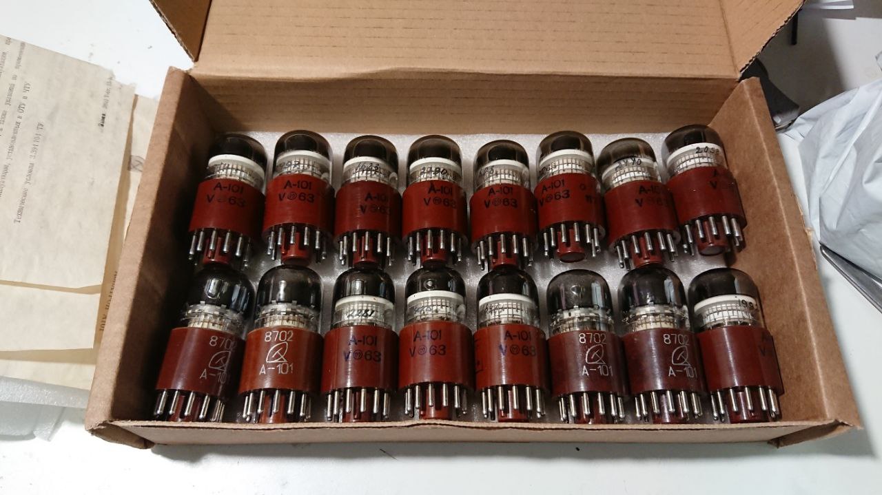
Figure 17: Commuting decatrons A101, A102 and A103
Although for this picture you can already guess what will be discussed.
Why is it ????

Links
The whole project continues to be completely open. Therefore, the main project links:
- A repository with concepts and layout of printed circuit boards . The firmware of the indicator module and the memory card are also located there.
- On this page I publish weekly and not so reports about what has been done. You are currently reading an article that is slightly more than fully composed of these notes. With translation, comments and additions.
- Compiler and emulator .
')
Source: https://habr.com/ru/post/411145/
All Articles