Trust and Verify: Approach to Verifying Circuits and Printed Circuits
Creating electrical circuits and tracing printed circuit boards are becoming increasingly simple. Component manufacturers integrate more and more functionalities into products, lay out ready-made models, conventional graphic symbols (UGO) and whole schemes, sites automatically generate power supplies, filters and much more. Nevertheless, even when designing simple printed assemblies, errors are detected, often stupid and obvious.
Today we will not talk about DRC and ERC , they should always be done and everything is more or less clear to them (if not, write in the comments). We will talk about verification by man.
When the next “last” time, before being sent to production, you leaf through layers in your board, the picture is already so familiar that the eye misses mistakes. To check the need for "second eyes" - it's time to call another engineer.
When you are for those who have these “second eyes” - the circuit and the board is completely new, and all the unusual catches the eye. However, a non-systematic check does not guarantee a total viewing of dangerous places, which can lead to a delay in the timing of debugging and to additional iterations not covered by the budget.
With the awareness of these limitations, we introduced a checklist that allows us to cut off the most common mistakes. About him today and I will tell.
There are almost no highly specialized items in the list - we are doing many diverse projects and the list is universal. For all difficult places in the digital circuitry has its own checklists, which give manufacturers of chips.
Operating procedure
According to the author, as soon as the scheme or board is ready, it sets the Redmine task of checking for another engineer (Reviewer). The reviewer, in addition to possessing knowledge and experience, should study the TOR and all additional project materials. All this takes a lot of time, which should be allocated at the planning stage of the project.
Having finished acquaintance with the documentation, it is necessary to be adjusted on a correct harmony. Verification is an aid in achieving the best possible result. Before you come down with criticism, it is important to remember that the engineer tried to do his job excellently, “from the heart,” and the task of the inspector is not to disturb this mood.

The reviewer copies the text of the checklist from the Knowledge Base to the comment to the task, and then moves through the list, leaving its notes. The following symbols are used:
- “+” And “-” to state the passage or non-applicability of an item,
- bold for obvious mistakes,
- italics for recommendations and questions.
After reviewing, as a rule, there is an oral discussion of comments, clarification of unclear points, and as a result, comments are often corrected.
Further the text of the list from our Knowledge Base, comments for you are in italics . In the list there are some points specific to Altium Designer.
For multipage schemes, the division into sheets, for one-page all items apply to one sheet. (As a rule, we use hierarchical multi-page schemes; for such schemes, for each sheet it is necessary to repeat the check “Block”, renaming “Block” into the name of the sheet of the scheme)
Check for new components
- Check by list from task (When setting the task for review, the author creates a list of newly created components so that the Reviewer does not miss anything. It is considered that the other components have already been checked by us earlier.)
- Check by datasheet:
- Contact numbers
- Purpose
- Matching references to descriptions (the link to the description of the component must be in the properties of the component)
- Seat (must match the specified partnumber)
- Partnumber (fairly complete, no errors)
First sheet
- Check project settings:
- revision (Field revision in properties - later used to generate documentation)
- compiler settings (db. configured in the project by default) (Altium compilation settings - what is possible, what is impossible. Usually we create a project from an internal template, in which everything is already well tuned)
- Compiling a project (are there any errors)
- Connectors: (rely on TK and additional wishes in the spirit of “like on the XX board”)
- type of
- pinout
- correspondence of the number to the number on the diagram
- Blocks on the first sheet:
- coverage of the functional (All functions described in the TOR are implemented)
- quantity if multichannel
- synchronization of character sheet outputs
- Registration (Registration is important. The unfinished scheme does not pass validation)
- Title block
- Location of blocks, signatures, communications
Block
(As a rule, a block is a simple circuit, often from a single chip with strapping)
- The correctness of the arrival of lines of interfaces
- UART Rx-Tx - crossed at the "slave" (This legendary error deserves a separate line, although in the paragraph all interfaces are checked)
- The correct supply of power (power required nominal, the earth comes to earth, analog power to analog, etc.)
- For any microcircuit - check on Datasheet: (Here we most often appeal to the typical inclusion scheme)
- Purpose
- FT (tolerance to 5V and other voltages at the feet of the controller)
- Other (bad item)
- On each sheet - a list of used meals, the maximum consumption of them (used to summarize the requirements for power in the device)
- Designation of classes of chains for the allocation of specific places (for example, isolation)
Power scheme
- The list of used feeds, consumption (take from all blocks and fold)
Near each source: (In simple schemes there is no requirement)- Output voltage
- Current
- Efficiency
- Power dissipation
- Designation of classes of chains: HV, Power, ... (All that is useful for tracing)
- For each source, check the inclusion scheme for Datasheet
Transfer to check for programmers
- Prepare documentation (Scheme and List Generation in pdf)
- Create a task for checking the scheme for programmers (Programmers have their own list of checks)
Design
If there is a 3D model for the device, a check is made on it. (Most often the device is assembled together in 3D CAD, there are tools for checking interferences, performing cross sections, etc.)
- Board form - Compliance to the drawing, models, TZ
- Board thickness
- Fastener
- Sufficiency (in terms of compliance with the item TK “external influencing factors”)
- Getting into places on the board
- Clearance for screw heads, washers ...
- Connectors
- Position
- First leg orientation
- Check pinout with articulated boards
- Position of specific components
- Component height
Check connectivity project
(Commands for Altium Designer, the essence is to check that there is no difference in the board and the scheme)
- Design-Import Changes from PrjPcb: There Should Be No Differences
- Design-Update Sch in PrjPcb: There should be no differences
- Project-Component Links: The first two columns must be empty (In Altium Designer, sometimes components lose connections due to renumbering, inserting something on the board, etc.)
Seat check
- Availability of a list of new (updated) seats. When re-checking the list should be new. (The principle is the same as for HBO)
- Seat verification with description in Datasheet
- The order of the findings
- amount
- Distances
- Form pads
- Silk-screen printing 0.2, the first leg a circle thickness 0.5, diameter 0.25 (registration is important)
- The presence of a 3D model, the coincidence of the legs, silk-screen printing with it (3D models allow you to additionally check the correctness of the seat, participate in the design and verification of the design, help to get beautiful render boards)
Design rules
- The thickness of the metallization layer (In the settings of the stack, everything must correspond to reality)
- Compliance with the design rules of technological standards for the selected board thickness and metal (minimum gap / conductor, holes)
- The presence of specific standards for classes of circuits identified in the diagram (gaps to high voltages, minimum thickness of conductors, etc.)
- Indents from non-metallized holes in the inner layers (different from the usual gap)
- View all rules (All rules are viewed one by one, search for all unusual)
- DRC settings (checking if the necessary checks are included in the DRC)
- DRC (Reviewer launches DRC; if not, the test stops)
Nutrition
- The general logic of the location of sources and loads (Layout should be logical, not to cause complications to the board)
- Powering complex consumers through each other (One source for several consumers that can interfere with each other)
- Continuity (bottlenecks) (thin jumpers at polygons, number of vias when going from layer to layer)
- Section of conductors (Illumination of all the power supply in turn, viewing the leads to each consumer)
- Earth (Earth is very important if the current flows through the power bus to the consumer - he needs to go back)
- Leads between feeds, neighborhood of sources
- Chip Power
- The presence of blocking pins
- Thickness of power conductors
- Separate Via for each consuming pin
- Via ThermalPad (sometimes needed)
- Power sources
- Open Datasheet, check with the recommended topology (when it is not, discuss the optimal layout)
Signals
(This block describes the sequence, and even that is not complete)
- Clocks
- Diff pairs
- Fast signals
- Are common
Silk screen printing
- Default font, height 1mm, thickness 0.2mm
- Proper placement of labels - not under the hulls, not on the holes, not on each other (It is convenient to look in 3D)
- The orientation of any inscriptions on one layer is only 0-90 or 0-270 degrees
- The designation of the first pin in the chips and connectors
- Designation of 5-10 multiple pins and rows for BGA for large chips (helps to find the right pin for debugging)
- Designation of connector assignment and test points (helps with debugging)
- Competent sequence in groups (when designations are put aside by the group due to the density of the components)
- Logo, name of the board, SVN revision, date (Often there is a customer's requirement for placing your logo, decimal number, etc. AD allows you to set text fields defined by variables, we actively use it)
Other
- In the hole editor, view all holes (for anomalies)
Check lists gradually evolve, new items are added, unnecessary items are removed.
Checking the lists allows us to find a lot of mistakes every day, and it was not so scary to send fees to production.
How do you check your fees? Share in the comments.
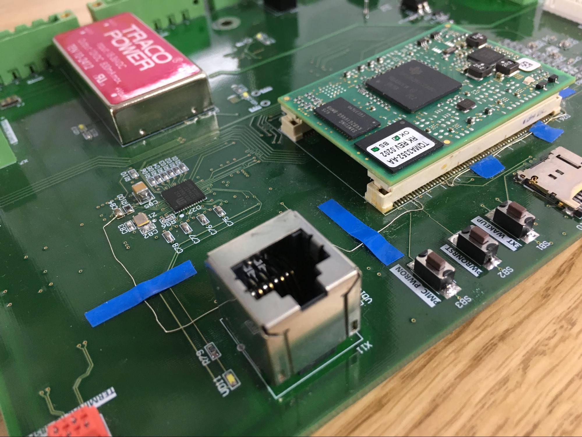
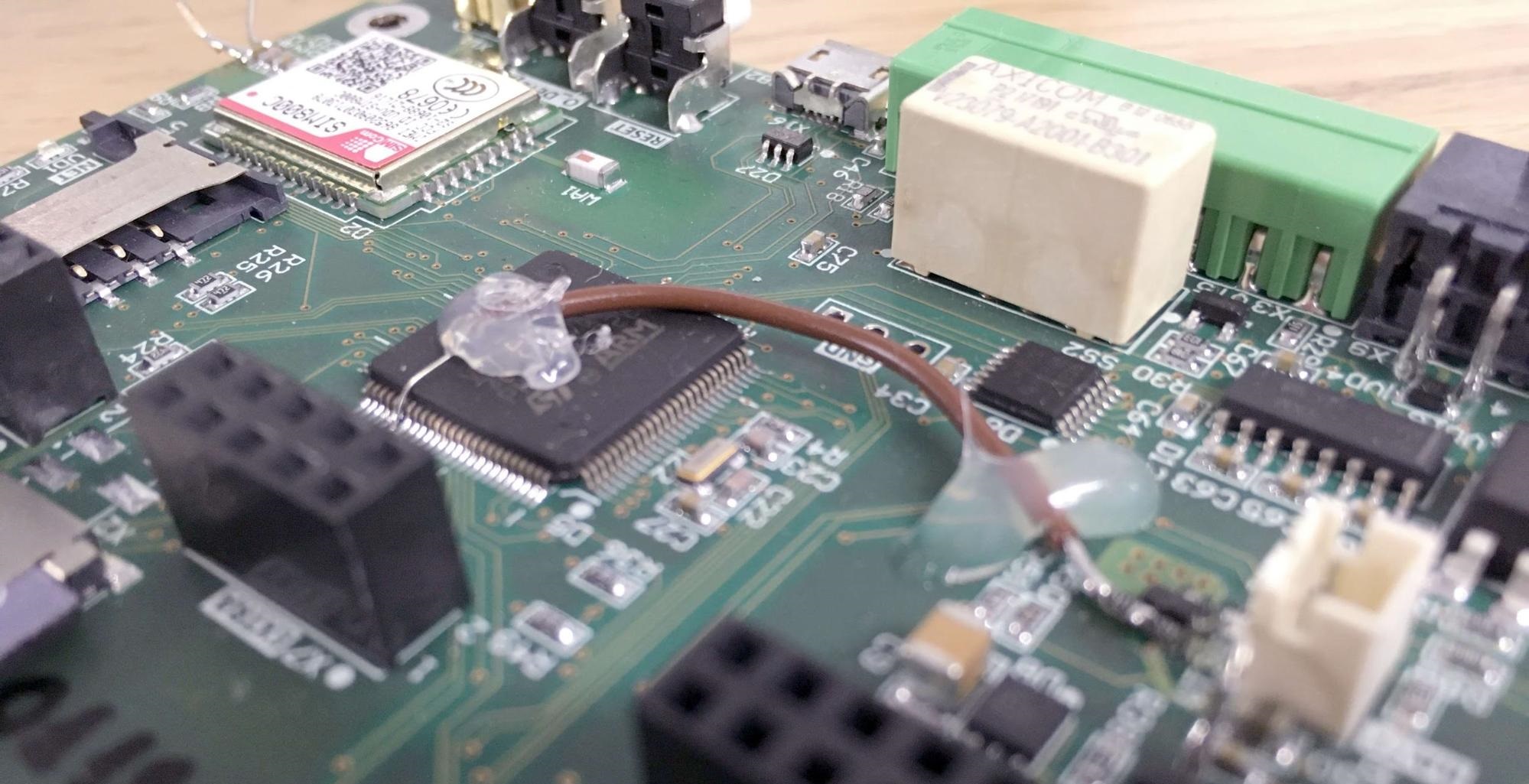
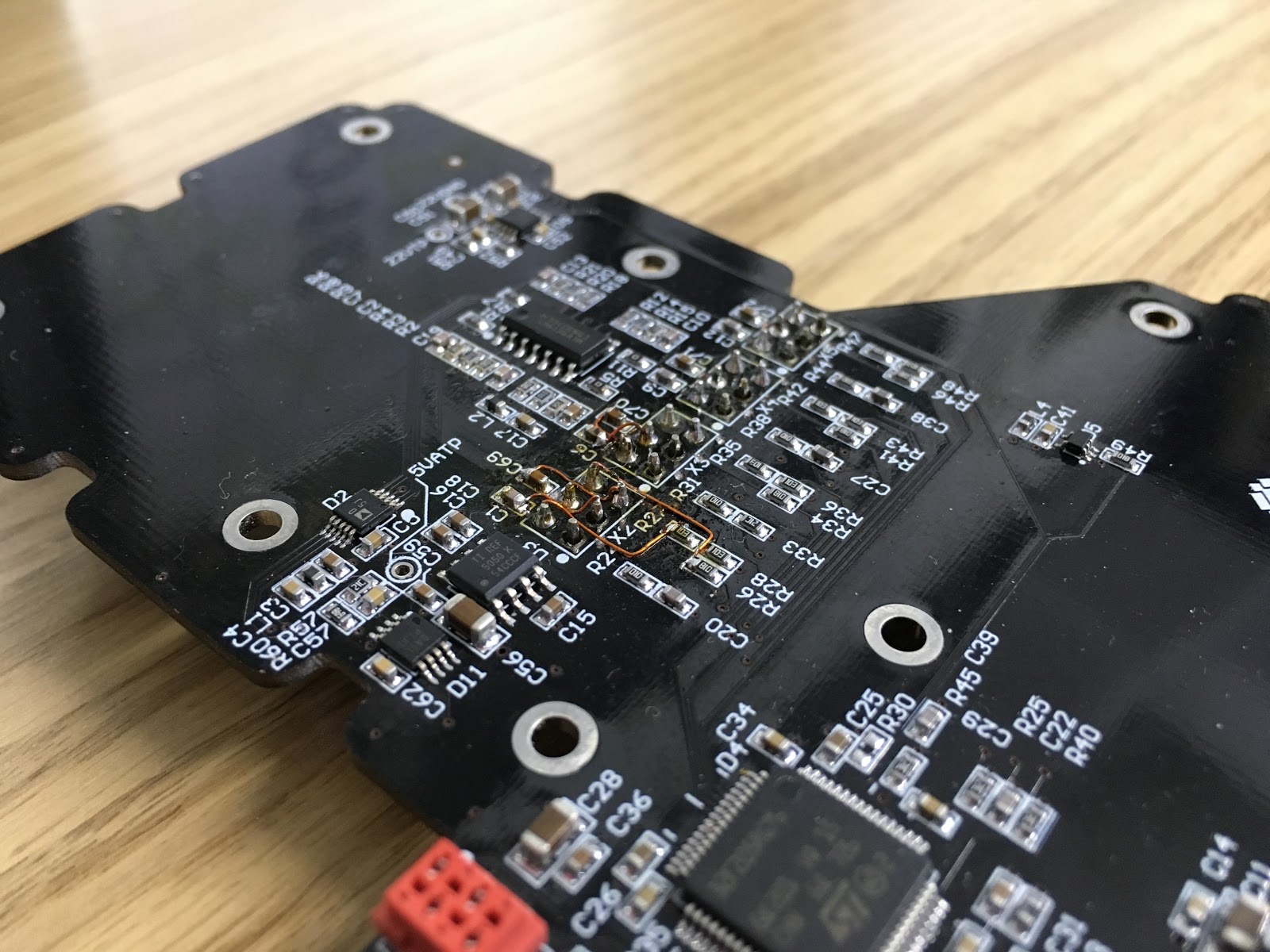
* The last picture in the text illustrates that even a thorough check will not save from an inattentive customer.
Read on
')
Source: https://habr.com/ru/post/410853/
All Articles