Semiconductor industry: the transition to process technology 10, 7, 6 and 5 nm
Samsung semiconductor factory in Austin (USA)
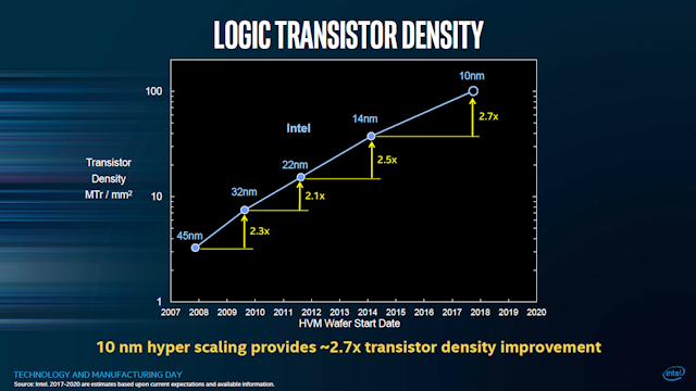
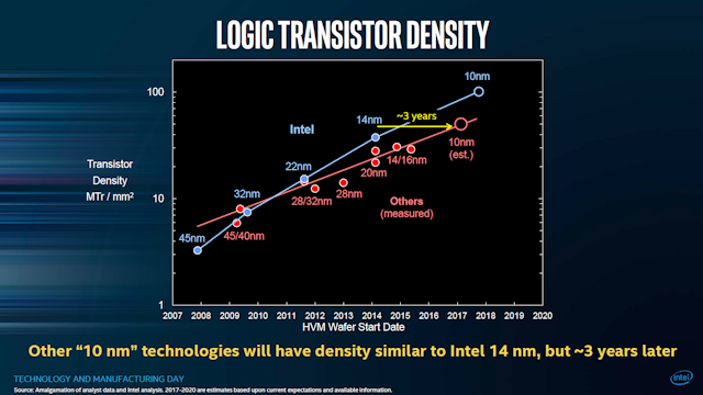
The transition from 14 nm to 10 nm will be the largest technological jump in the density of transistors in history. The density increases immediately by 2.7 times. Thus, Moore's law will continue in the coming years. AnandTech has put together information on the plans of various companies for the construction of new generation plants with technical processes of 10, 7, 6 and 5 nm.
')
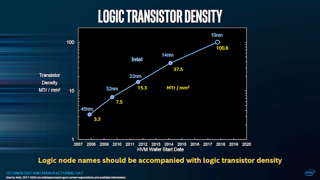
It must first be noted that measuring the density of transistors by the size of a single transistor is not a completely correct metric. For example, Intel has calculated that its 14 nm fits 23% more transistors than 14 nm from other companies. This difference is due to the smaller height of the logic cell, the smaller distance between the gates and the smaller edge pitch (see table).
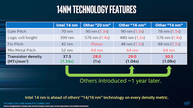
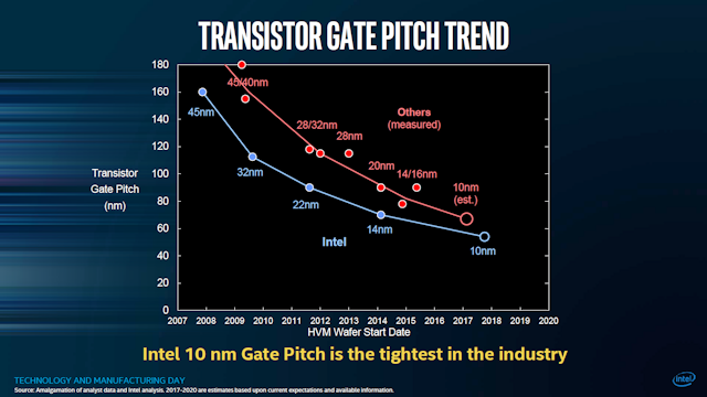
For example, the gate pitch (gate pitch, the distance between the gates of neighboring transistors, including the width of the gates themselves) is significantly less for Intel than for other manufacturers. On the 22-nanometer process technology it was about the same as the competitors are now at 14/16 nm.
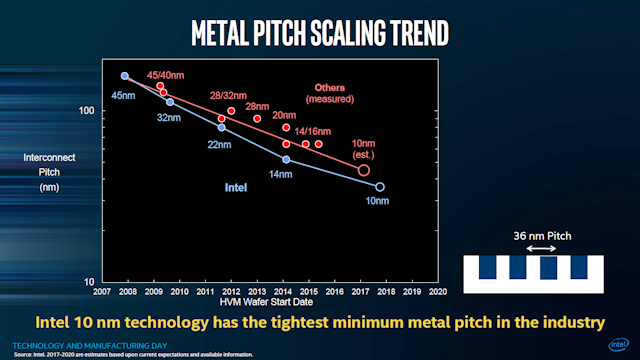
At the interconnect pitch (interconnect pitch, the minimum distance between the layers of in-circuit connections), Intel does not have such a cardinal advantage, but all the same, the competitors are still not close to the figure that Intel has already reached at 14 nm.
Thus, the “other factories” will achieve an “Intel” density of transinistors with a delay of three years: for this they need to implement a 10 nm technical process to equal 14 Intel at 14 nm, and the leader himself will then go far ahead. At least, such plans at Intel.
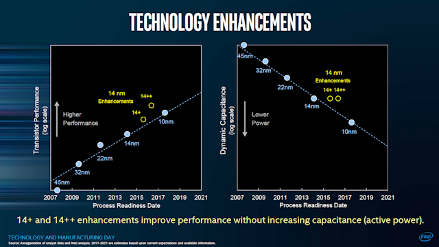
Interestingly, Intel’s third-generation, advanced third-generation 14 nm ++ technology will be better than the first 10 nm chip samples. The company itself recognizes this. Nothing can be done - new technologies still need to be tested and tested. That is, we can wait for the actual improvement in the 14 nm ++ technology somewhere around 2020, and we can only hope here for Intel, because the competitors are technologically lagging behind, despite the stated plans of 10 and 7 nm (again, again, this Intel's words, but what is actually the technological lag of competitors and whether it exists is unknown).
In fact, it would be more correct to consider the density of transistors in fact: divide the area of the chip by the number of transistors. But how to do it, if the factories themselves have not yet begun to work. Analyzing the plans of companies, you can only compare construction time with each other, equating the same rate of technical process for one company with the same parameter for another: 14 nm to 14 nm, 10 nm to 10 nm, etc.
AnandTech has collected information from all the major players in the semiconductor industry, who plan to invest in the modernization of production and construction of new factories. These are GlobalFoundries (USA), Intel (USA), Samsung (South Korea), Semiconductor Manufacturing International Corporation (SMIC, China), Taiwan Semiconductor Manufacturing Company (TSMC, Taiwan) and United Microelectronics (UMC, Taiwan). Their plans for the coming years can be summarized in the following table.
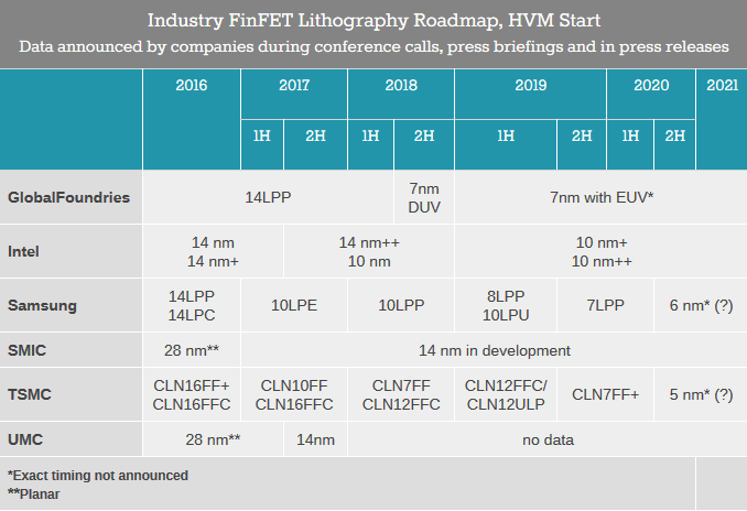
As can be seen from the table, GlobalFoundries will continue production using the 14LPP process for the next year, but at the end of 2018 it is going to begin mass production of 7 nm chips. The start of mass production and the start of sales of finished products is not the same thing. These two events can divide 4-7 months. First, GlobalFoundries intends to use traditional deep ultraviolet lithography (Deep Ultra Violet, DUV), which uses light sources with a wavelength of 193 nm, and then switches to improved EUV technology (Extreme Ultra Violet) with a wavelength of about 20 times smaller. At such scales, the wavelength is about several dozens of atoms, so EUV opens up fundamentally new opportunities in the semiconductor industry.
Intel will begin production of 10 nm chips for mobile devices already this year, although processors for desktop computers will remain at 14 nm for now. At the end of the year it is planned to set up production for the third generation of 14 nm ++. Intel is one of the first to invest in the study of EUV, but it is not making any specific statements about the use of this technology. It is understood that Intel will not use EUV up to 5 nm.
TSMC after the introduction of 10 nm plans to quickly go to 7 nm, and Samsung, on the contrary, is going to release 10 nm chips until 2019. The density of the transistors depends not only on their size, but also on the perfection of technology. Probably, 10 nm from Samsung will provide approximately the same density as 7 nm from TSMC. Here is the same situation as with the technological superiority of Intel.
Samsung plans to introduce a lithograph of the new generation EUV in the years 2019-2020 for the production of transistors such as CLN7FF +.
EUV experiments are conducted by many, but nobody still knows for sure whether it will be possible to ride this advanced technology. All the plans of companies regarding the EUV in the table so far can be regarded more as "desires".
Source: https://habr.com/ru/post/403917/
All Articles