Anatomy and cloning of the USB adapter for the SD card
... or how to supply your DIY project on MIPS or a light ARM with a fast micro SD card.
Good day to all respected community. I would like to continue my story about the box-device , namely, about how she managed to acquire a micro SD card connected to the USB 2 port.
The root of the whole problem was that USB 2, and not even one, its processor module has, and QSPI (QuadSPI) or a card interface - alas, no. How is this sad fact related to SD cards? Very simply, any SD card in the physical basis of its connection has an SPI (SerialPeripheral) interface. Classic SPI for transmitting and receiving serial data uses one physical line. Simple and economical, both in terms of money and milliamps. However, disadvantages, as is well known, are a continuation of the merits, and for SPI they first of all became a relatively low data exchange rate. To solve this problem, a four-bit mode of data exchange with an SD card was developed, which is a close relative of the QSPI protocol. When using this mode, the host controller and the card first agree on the exchange parameters in single-bit mode, and then go to four-bit when using not one line for receiving and transmitting, but four for everything about everything (plus one more to indicate the command).
What to do if the hardware does not directly support the four-bit protocol, but does it need a fast exchange? The obvious answer is to equip the project with a “fast interface” bridge - a “four-bit SD card”.
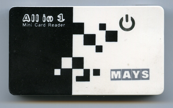
To solve this problem, a couple of USB-SD adapters were purchased and subjected to preparation (vivisection was not used - we are not what monsters). Before reheating a soldering iron and a hairdryer, a very important check was made to see if the Debian processor module sees the proposed whistle adapter. The test went off with a bang, welcome to the operating room. The bought whistle looks like this:
')

And so:

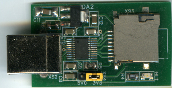
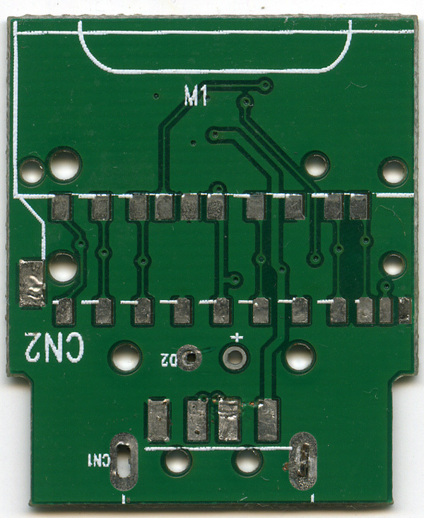
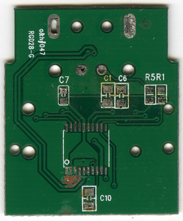
After the case was disassembled, it became possible to make out a printed circuit board (from all its two sides).


The scheme is simple, its basis is the IC GL823F - a microcontroller with an 8051 command system and with mask memory, equipped with a USB 2 interface hardware unit, apparently not of a very high quality (why do I say that - I don’t see the exact analog bias resistor and crystal oscillator , which means the restoration of the frequency of the received signal based on the internal calibrated generator). Will work, but not HiFi, no. Everything else - the minimum kit: blocking capacitors, pull-up and current-limiting resistors, LED and connectors, that's all engineering.
Blow off the components with a hair dryer and look at the printed circuit board. In many ways, the board is double-sided with plated holes. After a brief examination of the board in the microscope, drawing the wiring diagram and comparing it with the datasheet on the related ICs of the GL company, we restore the circuit diagram.
And here we begin to see one small hitch. What exactly? Our box is powered from a guaranteed voltage of 3.3V, and the GL823 circuit requires 5 volts. Well, as it requires - she was so used to it, because it is how much USB gives her. The micro SD itself is powered by 3.3V, so the built-in LDO stabilizer has been added to the GL823. Hence the question - and if the circuit is powered by 3.3V, then can it work? If an LDO is able not to drop the voltage too much, it can, but not all LDOs are equally useful. A little hint is given by datasheet — the output that powers the SD card is called PMOS. Such an abbreviation can not but rejoice - it can be assumed that the HighSide PMOS scheme is used, in which the voltage drop on the regulating element can be very small. However, all this is reasoning, and the only decisive argument is experience, it is the son of difficult mistakes.
So what kind of experience will we put? Let's try feeding the IC with two switchable voltages - from 5 V USB or from 3.3 V, received by a separate stabilizer. Now we have enough knowledge to draw a schematic diagram.
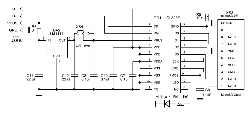
The numbering of the components in the diagram is somewhat strange for the reason that at the factory of printed circuit boards a multi-stock was ordered with several more test circuits, and all of them had a continuous numbering of components. Preparing the article, the concept I brought into line with the photo, and it turned out what happened.
What do we see in the diagram? Clearly, the core is GL823F. The micro-SD connector is obviously connected to it. The only thing to note is that the pin 9 at the connector is a sliding contact of the presence of a card in the slot, when the card is in place, it is closed to the ground. C7-C10 - blocking capacitors on the power supply. If you want to slightly increase noise immunity, then conclusions 2 and 16 of the DD1 can be connected via a ferrite choke. R4 limits the current through HL1, R5 pulls up the GPIO line to one in the absence of a card in the slot. DA2, C11 and C12 form a 3.3V linear voltage regulator.
Since at that moment, when the scheme was being drawn, on the one hand, it was not clear how much it would consume, and on the other there was an unpleasant experience of using some USB flash drives (it would not point with a finger) that consumed 400mA when recording, it was decided to add R6. In general, this is a standard technique - with a noticeable consumption in the linear LDO circuit (the keywords here are LowDropout), put a low-impedance high-power resistor at the input and dissipate some of the heat on it, and not on the stabilizer. Experience, however, showed that there is no need for R6, and you will see it later on the photo of the board.
XS4 is just designed for the experience - switching power DD1 between 5 and 3.3 volts. XS2 is a standard USBB connector, so that you can put it in front of you, and not climb to free USB ports under your desk to your PC.
Here is what happened after tracing, PP manufacturing and installation:
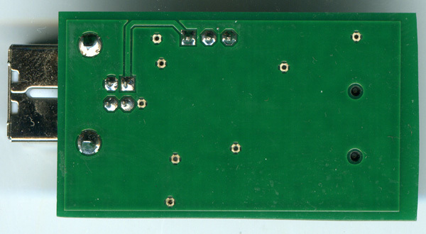
As you can see, the lower side of the board is completely uncomplicated, and the upper one is not much more complicated.
I am not going to delay the plot decoupling, I will say straight away that experience has shown that it is possible to power the GL823F from a 3.3V source without problems, switching the XS4 does not affect anything other than the power consumption (not current).
To make sure that the board made is working normally, the recording speed and current consumption for three different micro-SD cards was measured. Photo contestants - in the studio!

The evaluation of the current consumed (by measuring what was done, my language cannot be called naked) was carried out with the help of such a combined current-voltage meter-quantity of the battery charge. To be frank, some surprise for me was that it also transmits USB data.

Only the current consumption reading was used, the division price of this, if I may say so, device is 0.01A, plus at least a sampling error of 1 lower order digit is 0.01A. Therefore, the table shows only the ranges of indications between which the figure of current consumption jumped. I hope, however, that for those who would be interested to apply GL823 in their decisions, it will still be possible to evaluate the upper bar of consumption.
In addition to testing the board made, to improve objectivity, a couple of control measurements were made using another SD card reader. Here is this:
This sample was not prepared, I borrowed it from my daughter for 5 minutes, and if I had gutted it, I would have been gutted right there. One thing is for sure - the chip in it does not belong to the GL823 family, whose members know how to work with the SD standard so much, the multistandard is too tough for them.
The read-write speeds were measured in the simplest way: the same file with the size of 1058268 KBytes was written to and read from the test card. The control experiment (on another reader) was conducted only in order to eliminate system errors for one or the other decimal order, the data on it were not processed, I just made sure that approximately the times and currents of consumption fight with those obtained at the previous stage.

If you want to use the described scheme in your project, then when estimating consumption, make an amendment to the fact that the supply current came from a USB voltage of 5 Volts, but the GL823 was powered from a voltage of 3.3 V and the difference was 5-3.3 = 1.7 (and this is 50 % of 3.3) was simply lost on DA2. When powered from a centralized (and, I hope, pulsed) source of 3.3 volts, you get a decent savings.
Source: https://habr.com/ru/post/403199/
All Articles