My little relays: Brainfuck computer is magic
Introduction
A long time ago, when everything was big around, and I was small, I read Wojciechowski’s “Radio-electronic toys” book, burning with the desire to realize one or other devices described in it. So, in the already distant 2008 year, out of several dozen electromagnetic relays, a 4-bit ALU was assembled ( RCVM1 - Relay Digital Computing Machine - version 1 ) capable of adding and subtracting. And I thought then - what if you assemble a substantially larger number of relays and build a full-fledged relay computer? On the unhurried assembly of the relay, it took here only 8 years to reach the required amount, and I began to create.
Let me introduce you to your project to create a second version of a relay digital computer, code-named "BrainfuckPC" - a 16-bit computer with Von-Neumann architecture and a set of instructions for the Brainfuck language. Design work has been completed, and I am in the process of making this monster.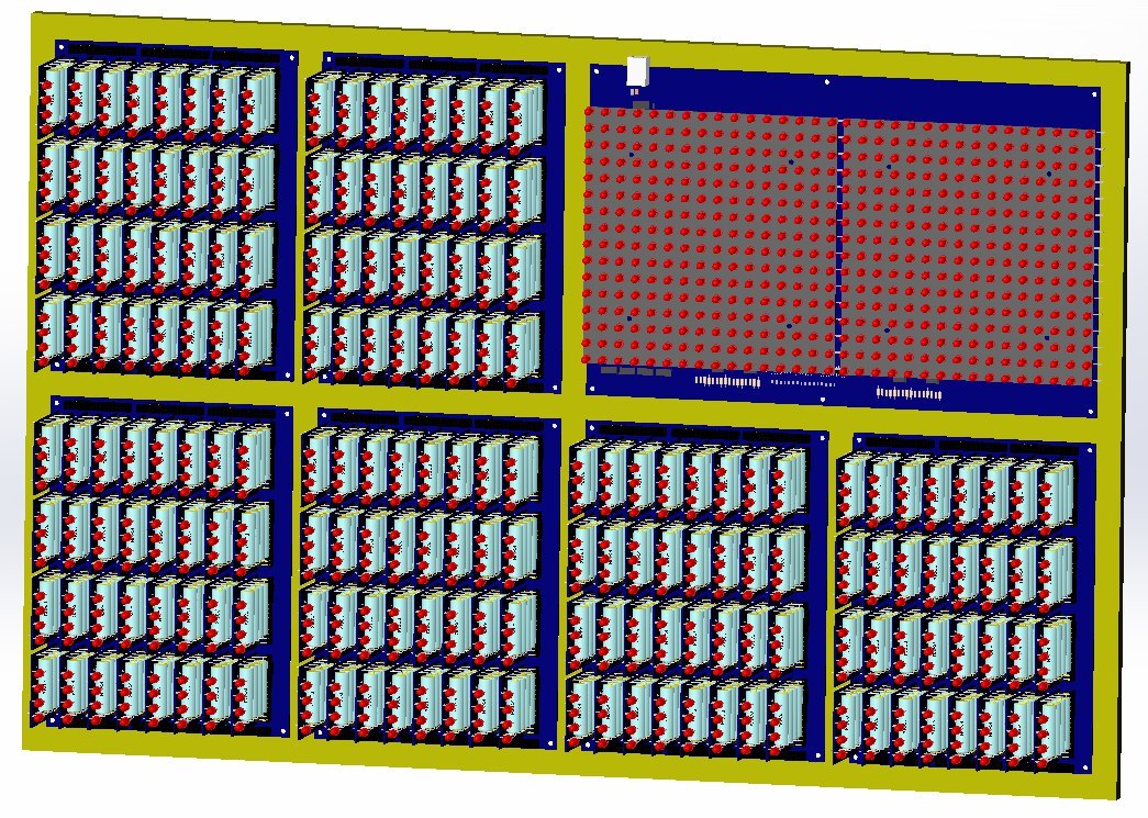
1 Specifications
- Address bus width: 16 bits
- Addressing: word for word, 16 bits / word
- Memory Capacity: 64 kiloslova (128Kbytes)
- Data bus width: 16 bits
- Single address code and data space (Von-Neumann architecture)
- Clock frequency (design): 100 Hz, 1 instruction / cycle
- Instruction Set: Brainfuck ++
- Number of relays (design): 792
- Used relays: reed, RES55 (1p), RES64 (1h)
Details tackle
General principle of work
Consider the generalized structure of the computer:
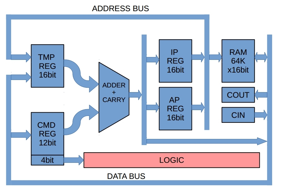
Figure 1: Generalized Computer Structure
The central element is the adder, and not simple, but with parallel transfer. Why this is needed - I will tell a little lower.
The program and data are stored in a block of memory. They are accessed at the address recorded in the IP instruction register, or in the AP address register, based on what we now want to read — the data at the address specified in the AP, or the instruction recorded at the IP address.
To operate this Turing tape (and Brainfuck, the programming language identifies it), we need to be able to do one of three things:
- To change the value in the current data cell, that is, to do the operations Add / Sub. In Brainfuck, the value in the cell can only be changed by one, i.e. +1 or -1. But having a full adder is a sin not to collapse long chains ++++++++++++ (------------) into one operation AP + = N ( AP- = N), significantly speeding up the process calculations. (also, let's not forget to turn [-] (or [+]) into * AP = 0);
- Change the number of the currently selected data cell. I mean, walking through the data memory (AP ++, AP--);
- Change the current instruction number. First, we need to increase the value in the IP register by one after the execution of each instruction. Secondly, to change this value in the presence of branches in the code (the default for the organization of cycles). The control flag is only one - Z. Accordingly, there are teams JumpIfZero and JumpIfNotZero.
In total, we need to be able to apply the value of any of the following three blocks to one adder - AP-register, IP-register, DATA-bus. We will do this through a temporary register in which we will save one of the required values, connecting the required one using 16-bit keys.
To the second input of the adder we will submit a number, to which one of these values should be changed in plus or minus. In view of the limited width of the instruction, you can only change to a + -12bit number. But for Brainfuck it is more than enough ("enough for everyone", yeah).
We will take these 12 bits from the register of commands, in the presence of such commands naturally, because some of the commands do not use an adder at all. Do not forget that negative numbers will be submitted in the amended code, with the filing of the add. unit transfer input (i.e., A + invB + 1)
The result of the calculation is immediately loaded to where we got it from. Because of the temporary register, we can do this without serious consequences.
In more detail (I would even say - boring) about the architecture can be found in this video:
Instruction set
Having drawn a general concept, capable of implementing 8 basic Brainfuck instructions, I realized that it has much greater potential. Therefore, I have developed a wider set of instructions that is compatible with Brainfuck, but requires compiling each original Brainfuck instruction into a 16-bit computer instruction.
General description of the instruction
All instructions are 16-bit. Formed from several parts.
- Bits 15, 14, 13 - determine the instruction class
- Bit 12 - Sign bit for sign instructions
- Bits 11-0 - contain the lower 12 bits of the signed int-a. The upper 4 bits are formed according to the value of the 12th bit.
Instruction table
| Instruction | Opcode | Operation | Equivalent of Brainfuck | Description |
|---|---|---|---|---|
| add m16 | 0X XX | AP ← AP + m16 | '+' (Repeat m16 times) | Adds a base to the current value of the selected cell. |
| sub m16 | 1X XX | AP ← AP - m16 | '-' (repeat m16 times) | Respectively subtracts the base from the number |
| ada m16 | 2X XX | AP ← AP + m16 | '>' (Repeat m16 times) | Increases address value |
| ads m16 | 3X XX | AP ← AP - m16 | '<' (Repeat m16 times) | Reduces the value of the address |
| jz m16 | 4X XX | (* AP == 0)? IP ← IP + m16: IP ← IP | '[' | Go to IP + m16 if the value of the current cell is zero |
| jz m16 | 5X XX | (* AP == 0)? IP ← IP - m16: IP ← IP | Not | Go to IP - m16 if the value of the current cell is zero |
| jnz m16 | 6X XX | (* AP! = 0)? IP ← IP + m16: IP ← IP | Not | Go to IP + m16 if the value of the current cell is not zero |
| jnz m16 | 7X XX | (* AP! = 0)? IP ← IP - m16: IP ← IP | ']' | Go to IP - m16 if the value of the current cell is not zero |
| and m16 | 8X XX | AP ← AP AND m16 | Not | Logical AND with a positive number |
| and m16 | 9X XX | AP ← AP AND m16 | Not | Logical AND with a negative number (someone must form the upper 4 bits) |
| or m16 | aX XX | AP ← AP OR m16 | Not | Boolean OR with positive constant |
| or m16 | bX XX | AP ← AP OR m16 | Not | Boolean OR with negative constant |
| in | c0 00 | * AP ← CIN | ',' | Read one m8 character from the console. If the input buffer is empty - wait for it. |
| out | c0 01 | COUT ← * AP | '.' | Print m8 character to console |
| clr.ap | d0 01 | AP ← 0 | Not | Clear AP register. Command allows combination |
| clr.ip | d0 02 | IP ← 0 | Not | Clear IP register. Command allows combination |
| clr.dp | d0 04 | * AP ← 0 | '[+]' or '[-]' | Clear the memory cell. Command allows combination |
| set.ap | d0 10 | AP ← * AP | Not | Write current value to AP register |
| set.ip | d0 20 | IP ← * AP | Not | Write current value to IP register |
| get.ap | d1 00 | * AP ← AP | Not | Read current value from AP register |
| get.ip | d2 00 | * AP ← IP | Not | Read current value from IP register |
| mode.b8 | e1 00 | Not | Activate 8-bit mode (1) | |
| mode.b16 | e2 00 | Not | 16-bit activation | |
| halt | f0 00 | Not | Stop machine |
- AP - Address Register
- IP - Register of Instructions
- * AP - Current Memory
- CIN - Console Input
- COUT - Console output
- When activating 8-bit mode, the adder continues to operate in 16-bit mode. However, the conditional commands (namely, the test value of the current memory cell for equality to zero) becomes 8-bit. ( AP & 0x00FF == 0)? and ( AP & 0x00FF! = 0)? Console input and output while decided to leave always 8-bit. Not in unicode to print in the end?
In this video, I described in detail (but little understood) what each instruction does and what kind of brainfuck instructions it corresponds to:
Parallel adder
A relay computer must be not only relay, but also fast. Like any other computer, mine will also be a synchronous machine equipped with a clock generator. Naturally, I would like not to waste the clocking cycles and try to fit each operation in one cycle - that is, for the rising and falling fronts of the synchronous generator, have time to load a new command and execute it. It is desirable at the same time that all commands were executed for the same period of time.
Each relay has a certain delay of operation and release, which we take for 1 conditional unit of time (cu). If we use the relay RES22, 1u.e. will be equal to 12-15ms (reference), RES64 - 1.3ms (reference). The most expensive (and most frequent) operation in my car is the adder.
By itself, it is quite simple and fast, but "there is one nuance", which consists in the method of calculating and transmitting the transfer signal.
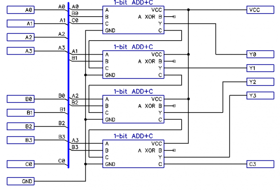
Figure 2: Adder with sequential carry.
I originally planned to use a sequential transfer adder. In such an adder, each subsequent discharge depends on the state of the transfer signal of the current discharge. As a result, the duration of the calculation operation will fluctuate between 2 USD. - N * 2 AU, where N is the number of digits. As a result, a 16-bit sequential transfer adder will have a maximum delay of 32 cu.
Parallel transfer adders have maximum performance. There are no processes for the spread of hyphenation from discharge to discharge. Output values are simultaneously generated in each digit:

Figure 3: Parallel Transfer Adder
The ability to build an adder with the specified properties is based on reproducing the sum and transfer functions that depend only on the values of the terms, regardless of the location of the discharge in the discharge grid. The catch is that the parallel transfer scheme itself becomes more complicated with each successive discharge. Here, see what happens:
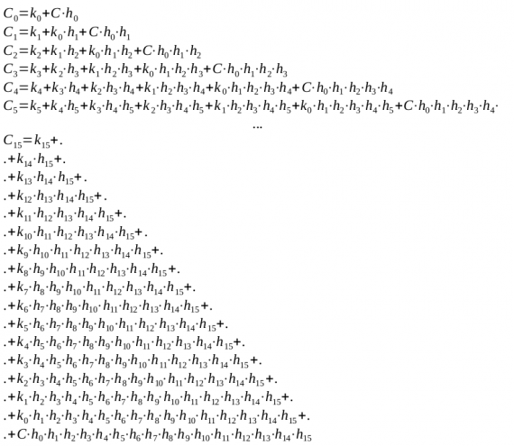
Figure 4: (Which should have been in the form of a LaTeX formula, but not) The transfer signal calculation equation for the bits. Where - bitwise AND, - bitwise OR
As a result, implementing a parallel transfer is quite expensive. However, it can be noted that the subsequent discharge contains the equation for calculating the previous one (there should be a meme "yes okay" with Nicolas Cage), so in principle it will be enough to make a transfer calculation scheme only for the senior level, and collect the rest from it, providing output intermediate results.
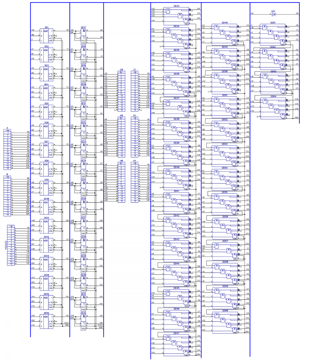
Figure 5: The complete circuit of a 16-bit parallel-transfer adder
In Figure 5, the first two columns are the adders themselves. Then come the 2AND and 2OR blocks, which form the intermediate values of h and k appearing in Figure 4. Their presence prompted me to expand the list of commands with logical addition and multiplication, for which I need to add only a couple of latches and the corresponding microcode.
Everything else is 5AND units based on 4 RES64 relays, which can be soldered so that one module can be used, for example, 2AND + 3AND. These blocks each logical step And output through the diode, which allows you to collect intermediate signals transfer.
Estimated signal propagation time: adders cope for 1 $, at this time, signals are generated at the outputs of the 2AND / 2OR units, then, 1 $. - multiplication in 5AND blocks, logical addition on diodes, does not introduce a delay. Well, the last one cu. spent on the calculation of the adder.
Total 3 cu. suprotiv 32, or not more than 4.5 ms to work the adder.
Registers
In the car, four 16-bit specialized register. No RON s. Only a tight binding, only hardcore! It consists of D-flip-flops, each D-flip-flop is a separate module for 4 RES55 relays with the following scheme:

Figure 6: Schematic diagram of the module D-trigger. Somewhere there is another connector, but here it is not important, because everything is signed.
The data comes to the Data input, the relay of which determines where the synchronization signal goes - to reset the trigger, or to set it (for which two more relays are responsible, one with self-blocking). The fourth relay gets the switching output Q. A very useful feature.
Memory board

Figure 7: Memory Board. Board dimensions 315x200mm
A very complex and important element, although the memory scheme itself constitutes a small part of the total filling of the block. The task of this board is, first of all, to carry 64 kilograms of shared memory of programs and data. It is assembled on the basis of two 64 KB cache chips. The address input through the protection circuit and the switch connects to the computer address bus, and from the data bus side there is a complex system from the input buffer and the output driver, also with the switch. Two lines W / R and Sync are responsible for reading and writing to memory. The first chooses what we will do, the second will actually do it.
And while this Sync itself is gone, the memory board naturally lives its own life. On the render you can see two 16x16 LED arrays. This display displays some memory. A kind of VideoRAM, determined by software, by the way. Interrogates the memory chip and controls the output of the Atmega1280 microcontroller.
For this task, the microcontroller does not end. It hangs console input and output. Where it will lead to - I have not decided yet, therefore, the motherboard is divorced with a USB-Serial converter for a regular console and ESp8266 for Wi-Fi. According to the latest, the most relevant plans are to have a web page with the ability to download programs for a computer into memory and the console itself. Yes, the tasks of the MC also include the initial download of the program to the RAM, for which it has full access to the RAM, as well as a small 1Mbit EEPROM for storing programs.
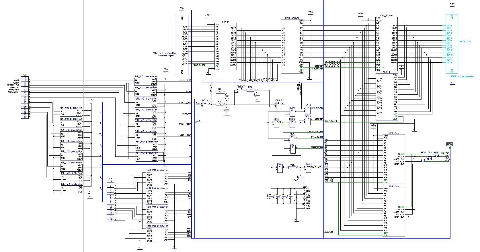
Figure 8: Schematic diagram of the memory board. Microcontroller and block circuit not shown
Logic block
I have no idea how it will look like in the end. The latest version is present on the general scheme of the computer, but I do not like it. Most likely I will do a 12-step sequencer and with the help of the keys I will send signals to separate blocks.
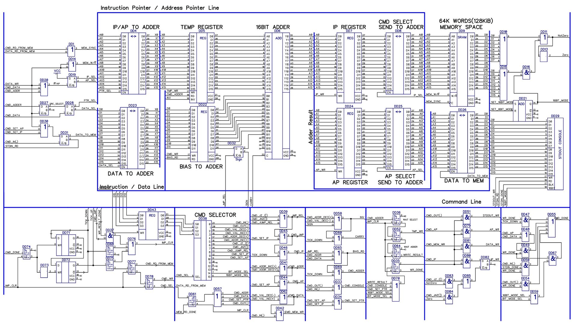
Figure 9: Everything around the 16-bit blocks is the logic block.
Design
The machine is modular, block-frame. On it is visually shown as the stuffing of the car will settle down. But first things first:
Module
The basic element of the computer is a 60x44mm module, with a 16-pin connector, carrying 4 relays, their binding, and 4 LEDs for indication:

Figure 10: 3D model of the module
Modules of various types:
- 1-bit transfer adder - 16;
- Module 5AND for parallel transfer scheme - 32 pcs;
- D-flip-flop module - 64 pcs per registers, plus a bit of logic;
- Module 4x2AND_SW, for the organization of latches. There are just 4 closing relays;
- 4x2AND module, for the organization of latches. Here are 3 relays of 4 with a changeover contact. 4 relays did not have enough output connector;
- Diode module, 8 D226D diodes. To organize a multi-input OR
- The universal 2AND / 2OR module allows you to create 2AND-NOT, 2OR-NOT, 4AND, 4AND-NOT, 4OR, 4OR-NOT and any combinations. Based on 4 relays with switching contacts and common points;
Since I invented the control logic block, I already rejected it, I don’t know the exact number of modules of each type. I'll figure it out on the way. The estimated number of modules - 192 pieces.
Block
We take a 150x200mm board, solder 32 connectors for 16 pins on it, and not simple ones, but install it with wrap and install our modules on an 8x4 matrix, getting such a block:
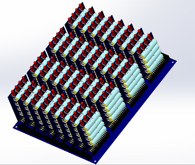
Figure 11: Block
In my car there will be 6 such units - two blocks for an adder, two for registers and two for logic. Scratching a turnip for a couple more blocks of latches, but if they do, they will be flat and soldered
Wrap-up installation was chosen because: firstly, the circuitry of each baseboard is known in advance, but it can be changed and error prone. Secondly, in principle, it is impossible to dilute a block of logic from the first time correctly, and if everything is clear for the block of registers as a whole and one can make a mistake with, say, a synchronization line, then the logic will have to be redone a thousand and one times. It will be much better if you build each component of the logic block gradually. Thirdly, it is a purely mechanical factor - it is physically impossible to separate these blocks on a double-layer board :) 16-bit tires diverge in all directions, which intersect with each other many times.
Total each block contains 32 modules, with a total number of relays 128 pieces. Power supply of each unit - 5V 2A.
Computer
On a large frame, 640x480mm in size (in fact a little more, but a beautiful number) six relay blocks and a memory board are placed:
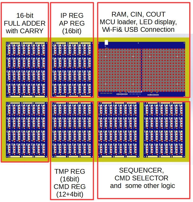
Figure 12: Machine Block Arrangement
The entire computer is inserted into a wooden frame of precious wood, with glass in front and behind.
Manufacturing
Despite today's date, the project actually exists :-) And is not in the most active, but still the manufacturing stage.
Relay
I have them. In large quantities, but the problem is that out of a more kilo-tight supply there are three hundred - a 27-volt relay and a 5-volt RES55 might not be enough for me. The scale of the disaster cannot be assessed definitively, but I think in the ensuing time that I will be collecting this hellish machine, the problem will disappear due to the replenishment of stocks from outside.
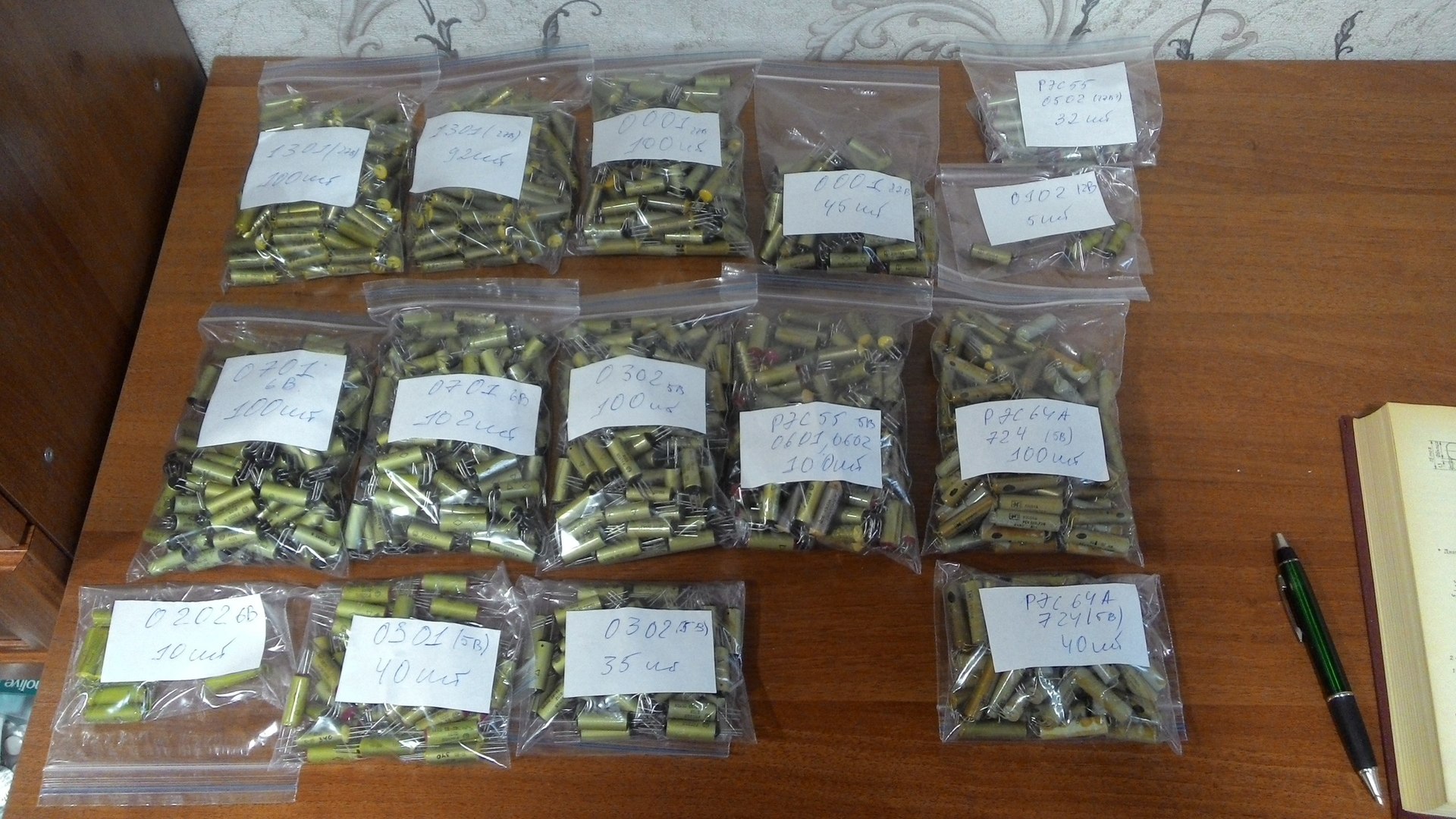
Figure 13: Relay Stocks. 800 relay units - new, successfully picked up at the Mitinsky radio market for a penny
One of the sources of replenishment of stocks are relay boards DAC from laboratory power supplies. Here are these:

Figure 14: Boards from power supply units of type BP, purchased on the radio market (no, I myself don’t bother with BPshniki)
Printed circuit boards
All the printed circuit boards I decided to do myself. I pinned 300 bucks to the Chinese and for 4 months I have been engaged in covering the workpiece with a photoresist, showing through, hounding, covering it with a solder mask, showing it, drilling it in a milling cutter.
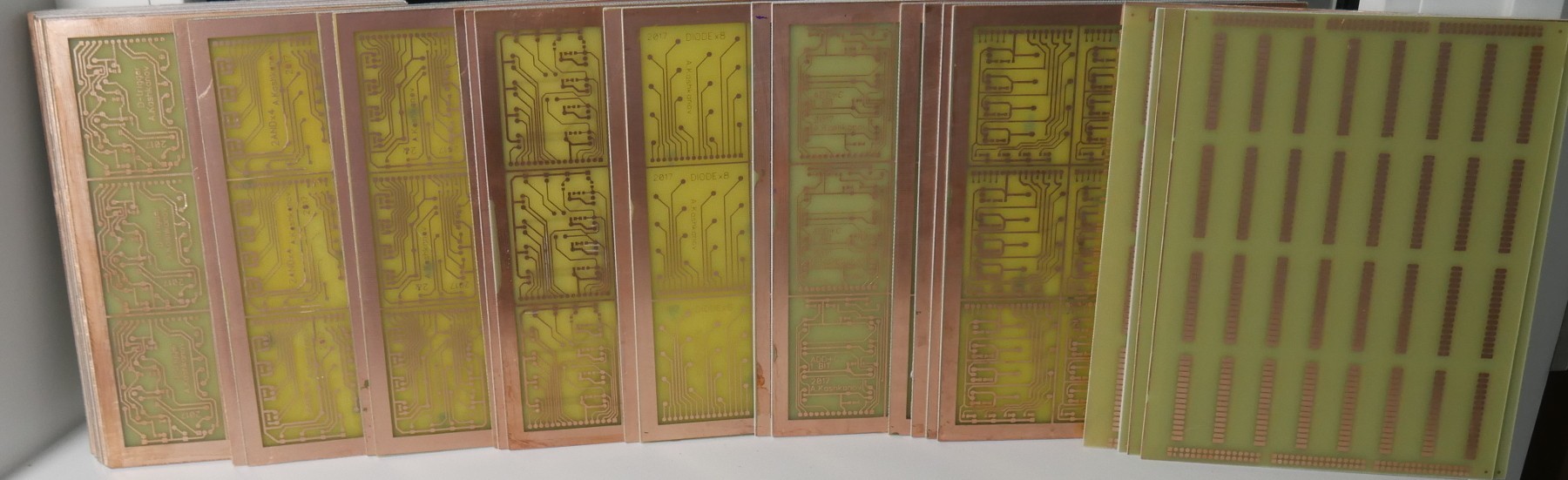
Figure 15: Etched Panels of Various Types
I make the boards with plates, 9 modules on a 200x150mm plate. Rinse 30 plates and stuck on applying a solder mask. All I can not begin. My solder mask for me is FSR-8000 blue, two-component and I have already dealt with it earlier.
Plates 200x150mm were not chosen by chance - on our radio market, in one secret place, such ones have been selling steadily for many years, and all of my adaptations are customized for this format.
In the word photoresist (MPF-VShch from Diazonium) I began to apply using a laminator and this is just miracles. The quality of bonding has increased significantly.
Then it will be necessary to cut and drill these boards, for which I even have a 3D router.
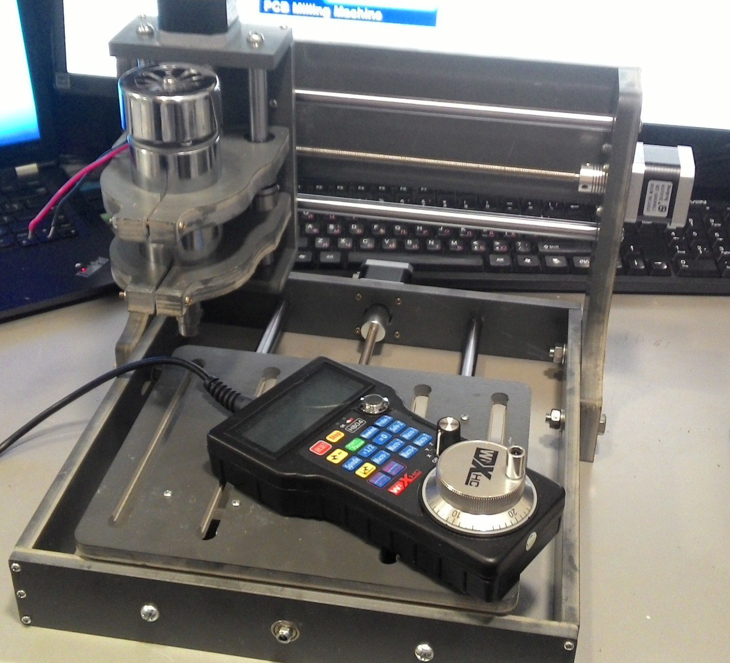
Figure 16: 3D Chinese milling machine DIY 2020CNC
I took it for a modest $ 175 exclusively for electronics. Boards to drill and mill will suffice, and I already glance at the sets of ball screw + rails for 3D machines. Ready to buy such a little expensive, and collect yourself when he begins to be required - the very thing.
Here in this review you can learn more about my machine:
Programs
Programs are loaded into the computer using a microcontroller, which means that he should know what and where to ship. For this there is a special format (in the state of the draft, of course) of the binary file a la Elf. The number, size and addresses of sections of code and data (as well as where the contents of these sections lie in the file) are written in the file header. // TODO Do not forget to add a section of video memory - we also have an LED panel, it is necessary to tell the microcontroller what kind of display it should be .
Having a microcontroller allows me to: a. control the correctness of the program, b. provide a secure memory mode. You can catch Segmentation Fault!
In general, you need a compiler. I tried dozens of different popular interpreters - everyone executes the same program in different ways. LeBrainfuck turned out to be the most stable , it does broadcast the program into its format and executes it correctly.
I wrote my compiler , at the moment its code is terrible, but it allows you to translate the usual Brainfuck into a binary format of my machine. Supports minimizing + - <> commands, but the conversion of the [-] sequence to cell reset is not implemented. Well, a bunch of other features, including support for add. instructions are also not made.
There is a simple emulator. The emulator at the time of this writing also supports only the basic 8 instructions. Here is what he does with the fractal program:

Execution time - a little less than 10 seconds. An adequate LLVM version found in the fields can cope in 0.9 seconds. About how I using Intel Vtune Amplifier optimized my emulator and clocked from 120 seconds to 10 deserves a separate article.
But it is not important. To derive this fractal, it took 3 billion optimized brainfuck instructions. Taking into account the design frequency of 100 Hz and 50 lines of text, we get 347 machine days - i.e. almost a YEAR per program, or a line of output per week! In fact, we will wait for the first line by the end of the first day, but the farther, the slower. On the other hand, it is the fastest on-off relay computer out of all existing and designed.
Behind this, the information is essentially over, so I suggest watching a small video review of other relay computers that exist in nature
Here is the most comprehensive in my opinion list of all relay machines at the moment.
Thoughts
I want to use a part of stocks of vacuum indicators IV-6 in the form of a long board in the upper part of the machine, which displays in real time the values of all the registers, as well as the total number of instructions executed and the total time of the computer. But here I can not decide on the source of this data - the MK in the memory board is packed to capacity, and it can only emulate some of the values. The best option is to read the values directly. According to the control scheme of IV-shkami themselves, I also cannot come to a unanimous opinion - it is more problematic to make a dynamic display of 30-40 IV-shek than for 6 pieces of a desk clock.
WHY? ???? 777

Links
The whole project in openSource. Therefore, here are the main links on the project:
- https://github.com/radiolok/RelayComputer2 is a repository with schematics and PCB layout. A link to the repository of the memory card firmware I will add later
- https://github.com/radiolok/RelayComputer2/blob/master/roadmap.md I will separately note this page with the project roadmap, on which key changes are recorded.
- https://hackaday.io/project/18599-brainfuck-relay-computer on this page I publish detailed reports about what has been done. On a set of critical mass, they will turn into an article on the GT.
- https://github.com/radiolok/bfutils compiler and emulator.
')
Source: https://habr.com/ru/post/402629/
All Articles