Milling of printed circuit boards at home
I do not like to persecute printed circuit boards. Well, I do not like the process itself fussing with ferric chloride. Print it here, press it, expose the photoresist here - the whole story every time. And then think about where to remove the ferric chloride. I do not argue, this is an affordable and simple method, but personally I try to avoid it. And then I had the happiness: I completed the CNC router. Immediately the thought appeared: would you try to mill the printed circuit boards? No sooner said than done. I draw a simple adapter with a crap esp-wroom-02 and begin my excursion into the milling of printed circuit boards. Tracks specifically made small - 0.5 mm. For if these do not come out - well, well, nafig this technology.
Here you need a small digression. There are several ways to get a set of gcode for milling a PCB from cad. In my opinion, they differ depending on which CAD system you use. If you are an Eagle lover, there are specialized and well-integrated solutions for it: PCB-GCode , the ability to directly open BRD files in chilipeppr. Unfortunately, not so long ago, Autodesk changed the licensing policy of the eagle, and now the community does not like it so much (you can see the opinion of one prominent member of the community ).
Since I personally make printed circuit boards every five years on major holidays, KiCAD is enough for me to design. For him, I did not find any specialized convenient solutions, but there is a more universal way - using gerber-files. In this case, everything is relatively simple: take the pcb, export the desired layer to the gerber (no mirrors and other magic!), Run pcb2gcode - and get the finished nc-file, which can be given to the frezer. As always, reality is a wicked infection and everything turns out to be somewhat more complicated.
Getting gcode from gerber files
So, how to get a gerber-file, I do not particularly plan to describe, I think everyone can do it. Next you need to run pcb2gcode. It turns out that it requires about a million command line parameters to produce something acceptable. In principle, his documentation is not bad, I mastered it and understood how to get some kind of gcode even so, but I still wanted to be casual. Because pcb2gcode GUI was found. This, as the name suggests, is a GUI for configuring the basic parameters of pcb2gcode with checkboxes, and even with a preview.
Actually, at this stage some kind of gcode was obtained and you can try to mill it. But while I was poking at the checkboxes, it turned out that the default depth value that this software offers is 0.05 mm. Accordingly, the board should be installed in the router at least with an accuracy higher than this. I do not know how anyone, but my desktop at the router is much more curve. The simplest solution that came to mind was to put sacrificial plywood on the table, to cut a pocket in it to match the dimensions of the boards — and it would be perfect in the plane of the router.
For those who already have a good router, this part is uninteresting. After a couple of experiments, I found out that it is necessary to mill the pocket in one direction (for example, feed per tooth) and with an overlap of at least thirty percent. The Fusion 360 offered me an overly small overlap and drove back and forth. In my case, the result was unsatisfactory.
Accounting for PCB Curvature
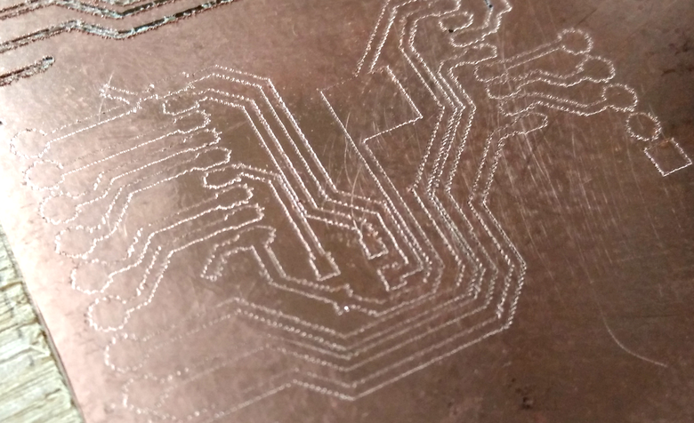
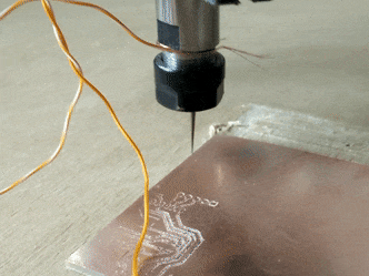
Having leveled the site, I poked a double-sided tape on it, put the textolite and started milling. Here is the result:
As you can see, from one edge of the board, the cutter barely touches the copper, on the other, it is too deep into the board, while milling the PCB chips went. Looking carefully at the board itself, I noticed that it was initially uneven: slightly arched, and, no matter how hard you try with it, there will be some deviations in height. Then, by the way, I looked and found out that for printed circuit boards with a thickness of more than 0.8 mm, a tolerance of ± 8% is considered normal.
The first variant of the struggle that comes to mind is autocalibration. According to the logic of things - which is much simpler, the board is copper-plated, a steel mill, attached one wiring to copper, another to a milling cutter - here’s a finished probe for you. Take it and build a surface.
My machine is driven by grbl on a cheap Chinese screen. The grbl has support for the probe on pin A5, but for some reason, there is no special connector on my board. Having carefully considered it, I nevertheless found that the pin A5 is connected to the SPI port connector (signed as SCL), there is also some ground there. With this "sensor" one trick - you need to twist the wires together. In the router it is extremely up to the fig interference, and without this the sensor will constantly give false positives. Even after interlacing will continue, but very much less.
So, the sensor is assembled, the tester is checked, then the important question is how to check in grbl that everything is in order and I won’t break a single engraver. A little googling showed that he needed to send the command G38.2 Z-10 F5.
The team says: start going down down to –10 in Z (absolute or relative height depends on the mode in which the firmware is now). It will descend very slowly - at a speed of 5 mm / min. This is caused by the fact that the developers themselves do not guarantee that the descent will stop exactly at the moment the sensor is triggered, and not a little later. Therefore, it is better to descend slowly so that everything stops on time and does not have time to go to pay for not indulging in the most. It is best to carry out the first test, raising your head to a height much more than 10 mm and dropping the coordinate system. In this case, even if everything doesn’t work and you don’t have time to reach the E-Stop button, the cutter will not be locked. You can do two tests: the first is to do nothing (and upon reaching –10 grbl will give out “Alarm: Probe Fail”), the second is while it is going down, to close the circuit with something and make sure that everything has stopped.
Next you need to find a method, how, in fact, measure the matrix and distort gcode as needed. At first glance, pcb2gcode has some sort of autoleveling support, but grbl doesn’t have support. There is an opportunity to ask the team to start the test hands, but with this we need to understand, but I, frankly, was lazy. An inquiring mind might notice that with LinuxCNC, the sample launch command is the same as the grbl command. But then comes the irreparable difference: all the “adult” interpreters of gcode save the result of the performed test to the machine variable, and grbl simply outputs the value to the port.
Easy googling suggested that there are still quite a few different options, but I came across a project chillpeppr :
This is a two-component system designed to play with WebNi hardware. The first component - Serial JSON Server, written on go, runs on a machine connected directly to the piece of hardware, and is able to give control of the serial port via web socket. The second one works in your browser. They have a whole framework for building widgets with some kind of functionality, which can then be thrust onto the page. In particular, they already have a ready-made workspace (set of widgets) for grbl and tinyg.
And chillpeppr has autoleveling support. Yes, and apparently it is much more convenient UniversalGcodeSender'a, which I used before. I put the server, launch the browser part, spend half an hour trying to figure out the interface, upload my board's gcode there and see some kind of garbage:
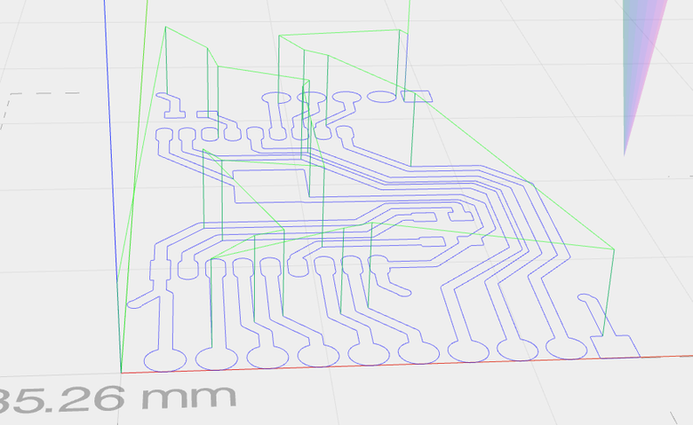
Looking at the gcode itself, which generates pcb2gcode, I see that it uses notation, when the following lines do not repeat the command (G1), but only new coordinates are given:
G00 X1.84843 Y34.97110 ( rapid move to begin. ) F100.00000 G01 Z-0.12000 G04 P0 ( dwell for no time -- G64 should not smooth over this point ) F200.00000 X1.84843 Y34.97110 X2.64622 Y34.17332 X2.69481 Y34.11185 X2.73962 Y34.00364 X2.74876 Y31.85178 X3.01828 Y31.84988 X3.06946 Y31.82249 X3.09684 Y31.77131 Judging by the fact that chilipeppr shows only vertical movements, it sees the string G01 Z-0.12 here, but does not understand everything that comes after F200. It is necessary to alter notation on explict. Of course, you can work with your hands or file some post-processing script. But no one has yet canceled the G-Code Ripper , which among other things knows how to beat complex gcode commands (like the same arcs) with simpler ones. He, by the way, is also able to bend gcode by the autoprobe matrix, but there is no built-in support for grbl again. But you can do the same split. The standard settings quite suited me (except that in the config I had to change the units of measurement to mm in advance). The resulting file began to appear normally in chilipeppr:
Then we run autoprobe, not forgetting to specify the distance from which to lower the sample, and its depth. In my case, I indicated that it is necessary to lower from 1 to –2 mm. The lower limit is not so important, it can be set at least –10, but I would not advise: a couple of times unsuccessfully set the starting point from which the test should be run, and the end points turned out to be outside the board. If the depth is greater, the engraver can be broken. And just a mistake. The level of the upper boundary directly determines how long it will measure the surface. In my case, the board almost never really went beyond 0.25 mm up or down, but 1 mm was somehow more reliable. We press treasured run and run to the mill, to meditate:
And in the interface chilipeppr appears slowly measured surface:
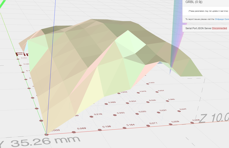
Here it is necessary to pay attention that all values in Z are multiplied by 50 in order to better visualize the resulting surface. This is a configurable parameter, but 10 and 50 work well, in my opinion. I often encounter the fact that any one point is much higher than can be expected from it. Personally, I attribute this to the fact that the sensor catches interferences and gives false positives. Fortunately, chilipeppr allows you to unload the elevation map in the form of a json'ki, you can fix it with your hands after that, and then load it with your hands. Next, click the button "Send Auto-Leveled Gcode to Workspace" - and in the pepper is already loaded corrected gcode:
N40 G1 X 2.6948 Y 34.1118 Z0.1047 (al new z) N41 G1 X 2.7396 Y 34.0036 Z0.1057 (al new z) N42 G1 X 2.7488 Y 31.8518 Z0.1077 (al new z) N43 G1 X 3.0183 Y 31.8499 Z0.1127 (al new z) N44 G1 X 3.0695 Y 31.8225 Z0.1137 (al new z) N45 G1 X 3.0968 Y 31.7713 Z0.1142 (al new z) Z motions added to the code that should compensate for surface irregularities.
Selection of milling parameters
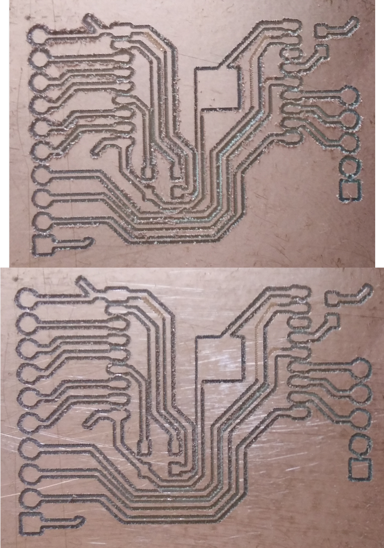
I start the milling, I get this result:
Here you can see three points at once:
- The problem with the unevenness of the surface is gone: everything is cut (more precisely, scratched) almost to the same depth, there are no gaps anywhere, nowhere has it deepened too much.
- Deepening is insufficient: 0.05 mm is clearly not enough for this foil. The boards, by the way, are some unknown beast with AliExpress, the thickness of the copper was not indicated there. The copper layer is different, the most common - from 18 to 140 microns (0.018–0.14 mm).
- The beats of the engraver are clearly visible.
About deepening. Pick up how deep it is necessary to lower the engraver is easy. But there is a specificity. The conical engraver has the shape of a triangle in projection. On the one hand, the angle of convergence to the working point determines how hard the tool is to break and how long it will live, and on the other, the larger the angle, the wider the cut will be at a given depth.
The formula for calculating the width of the cut for a given depth looks like this (immodestly taken from reprap.org and corrected):
2 * penetration depth * tangens (tool tip angle) + tip width We count on it: for an engraver with an angle of 10 degrees and a contact point of 0.1 mm with a depth of 0.1 mm, we get a cutting width of almost 0.15 mm. Based on this, by the way, you can estimate what the minimum distance between the tracks will make the selected engraver on the foil of the selected thickness. And still, even if you don’t need very small distances between the tracks, you shouldn’t lower the cutter too deeply anyway, since the fiberglass laminate is very hard on the cutters, even from hard alloys.
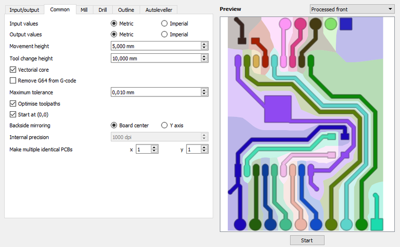
Well, there is still a funny moment. Suppose we have two tracks that are 0.5 mm apart. When we run pcb2gcode, it will look at the value of the Toolpath offset parameter (as far as retreating from the track during milling) and actually make two passes between the tracks by (0.5 - 2 * toolpath_offset) mm, between them will remain (or rather of all, a piece of copper will break loose), and it will be ugly. If we make toolpath_offset larger than the distance between the tracks, then pcb2gcode will issue a warning, but will generate only one line between the tracks. In general, for my applications, this behavior is more preferable, since the tracks are wider, the milling cutter cuts less - beauty. True, there may be a problem with smd-components, but it is unlikely.
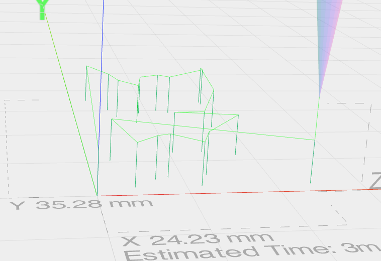
There is a pronounced case of this behavior: if you specify a very large toolpath_offset, then we will get a printed circuit board in mind of the Voronoi diagram. At a minimum - it is beautiful;) The effect can be seen in the first screenshot of pcb2gcode that I gave. It shows how it will look.
Now about the beats of the engraver. This is what I call them for nothing. My spindle is not bad, it seems, and so, of course, it doesn’t. Here, rather, the tip of the engraver, when moving, bends and jumps between the points, giving this strange picture with dots. The first and main idea - the mill does not have time to cut through and therefore jumps over. Easy googling showed that people are milling PCBs with a spindle of 50k revolutions at a speed of about 1000 mm / min. My spindle gives 10k without load, and we can assume that it is necessary to cut with a speed of 200 mm / min.
Results and conclusion
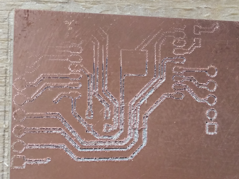
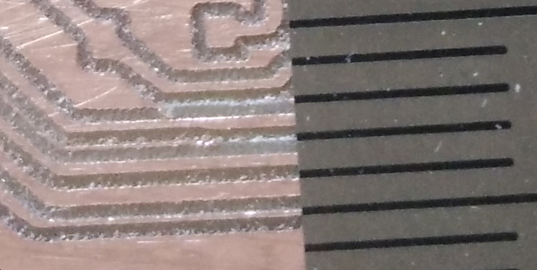
Taking into account all this, I am measuring a new piece of PCB, I start milling and I get the following result:
The top one is exactly the same as it came out of the router, the bottom one - after running the usual grinding stone on it a couple of times. As you can see, the tracks were not cut in three places. In general, the width of the tracks floats across the board. We still have to deal with this, but I have an idea what the reason is. At first, I fixed the board on double-sided tape, and it often went away. Then, in a couple of places, I grabbed more with the edges of the screws' heads. It seems to keep getting better, but still plays a little. I suspect that at the time of milling it is pressed against the platform and because of this, in fact, it does not cut through.
In general, the prospects for this all have. When the process is completed, building a matrix of heights takes about five to seven minutes, then directly milling - a couple of minutes. It seems you can experiment further. But then you can do the drilling on the same machine. Another buy rivets, and there will be happiness! If the topic is interesting, then I can write another article about drilling, double-sided boards, etc.
')
Source: https://habr.com/ru/post/402047/
All Articles