Almost universal converter on TPS63000, or catering for the smallest
Good day to you, dear geeks and sympathizers! For those who like to spend their free time on the development of
So, to begin with, we formulate a list of requirements for a power source:
')
1. Stable regulated output voltage from 1.5 to 5.5 V
2. Input voltage from 1.8 V (minimum voltage of two series-connected NiMH batteries) to 5.5 V (maximum USB voltage).
3. Power not less than three watts.
4. Automatic switching from boost (boost) to buck mode (buck) and vice versa.
5. High efficiency - efficiency not less than 95%
6. Compactness - in any case not wider than the diameter of a standard AA-size element
7. Minimum size
8. The minimum number of components, the absence of unreliable and rapidly aging electrolytic capacitors.
All these requirements are met by the TPS63000 integrated circuit. The only relatively inconvenient feature of this IC is its ultra-compact SMD VSON 3x3 mm case with eleven contact pads on the bottom side. The microcircuit does not need an external diode, and the dimensions of the cumulative choke due to the high conversion frequency are very small.
My option to turn on the chip looks like this:
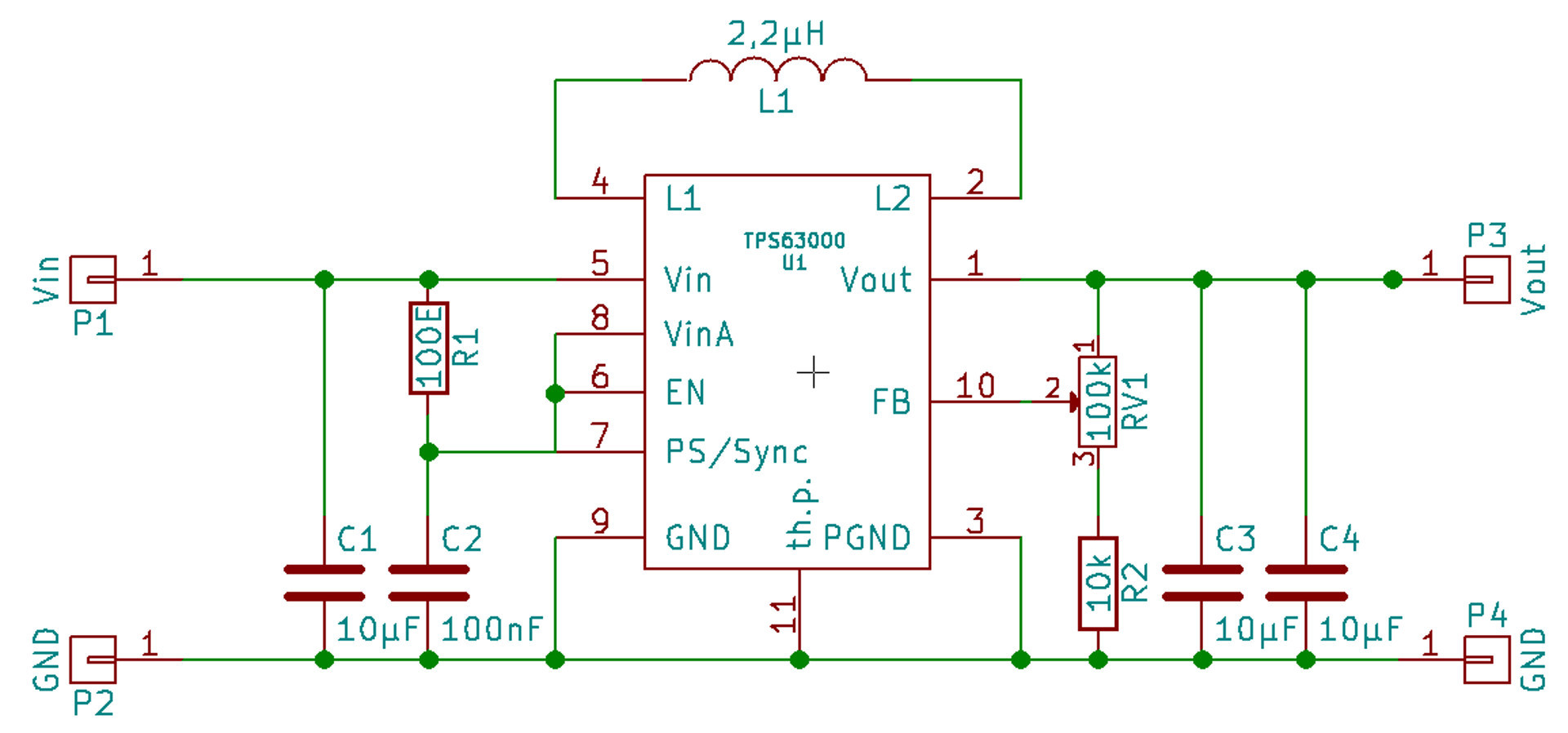
As can be seen from the above schematic diagram, the number of components is minimal, and they all exist in the performance of SMD.
A little about the properties and ratings of the components:
All multilayer ceramic capacitors, frame size 1206 with insulation material X7R and rated voltage 10 V.
Why is size 1206 instead of 0603 recommended in datasheet? The fact is that the desired compactness of the module and finding it in a closed case can lead to significant heating of the printed circuit board and components. Ceramic multilayer capacitors can lose up to 70% of their capacity when heated. This publication describes a significant improvement in the temperature stability of the capacitance of capacitors with increasing frame size. In addition, larger components are easier to solder to the board (with manual soldering, of course). Why the rated voltage of 10 V instead of the recommended 6.3 V? Because paranoia: for me, it is better to overpay a couple of cents, but to get more reliability than to destroy your nervous system due to a non-working device.
We now turn to the cumulative choke. Its size has been slightly increased compared with the technical documentation: instead of 4012, 4018 was used. This is explained. One of the most important parameters of the cumulative choke is the saturation current. Simply put, this is the magnitude of the current, at which the inductance of the choke begins to decrease sharply, and with a further increase in current, it turns into a piece of wire. The negative consequences of this: increased load on the control keys of the chip, the heating of the inductor, reducing the efficiency of the converter. For 4012, the saturation current ranges from 2.3 A (inductance reduction by 10%) to 2.5 A (inductance reduction by 30%), and for LPS 4018 it is already from 2.7 A (10%) to 2.9 A ( thirty%). The TPS63000 has a current limit of 3 A on the internal keys. Accordingly, LPS4018 is more suitable for
Accordingly, the heat loss in the choke will also be lower. By the way, in favor of choosing a choke with a large saturation current, the fact that with increasing temperature this parameter also deteriorates, and some stock will be completely superfluous, also speaks. Now about the choice of the inductor inductance value: in the technical documentation, an inductance of 2.2 μH is indicated as average for the average case, while it is mentioned that an increase in inductance reduces the voltage ripple on the load, but worsens the response to a load change. In addition, due to a heartless lady named physics, as the inductance increases and the size remains, the saturation current decreases and the resistance increases. In general, I did not increase the inductance value. How do I estimate the maximum current theoretically capable of arising in a choke? I use the most primitive method (damn, I'm just sure that there are special formulas for this!): To create a “point of reference”, we take the hardest mode - increase the voltage to 5 V, with a load of 800 mA DC. Accordingly, the output power is 4 watts. Four watts at 1.8 V (minimum input voltage TPS63000) means a direct current of 2.2 A. It seems that the choke 4012 should be enough in excess.
But in this case it is necessary to take into account that the pulse converter “pumps” half the time of the throttle, and the other half of the time “discharges” it into the load (this is, of course, a very rough description of the principle of operation, but for our purposes it is enough). Accordingly, to provide a constant input current of 2.2 A, a pulsating current of 4.4 A is needed. Since the internal keys of the chip are limited to 3 A, you can forget about conversion from 1.8 V and 2.2 A to 5 V and 800 mA . Given the imperfection of the components, losses and heating, 700 mA at 5 V at the output, respectively 1.5 A at 2.3 V at the input, is realistic. If you push off from 1.8 V input voltage, then the maximum output current at 5 V will be 500 mA. It is easy to calculate that in this maximum “inconvenient” mode for the chip, the output power will be only 2.5 watts.
The remaining elements of the device are not critical, resistors and 100 nF capacitor I took the frame size 1206 because of the ease of installation.
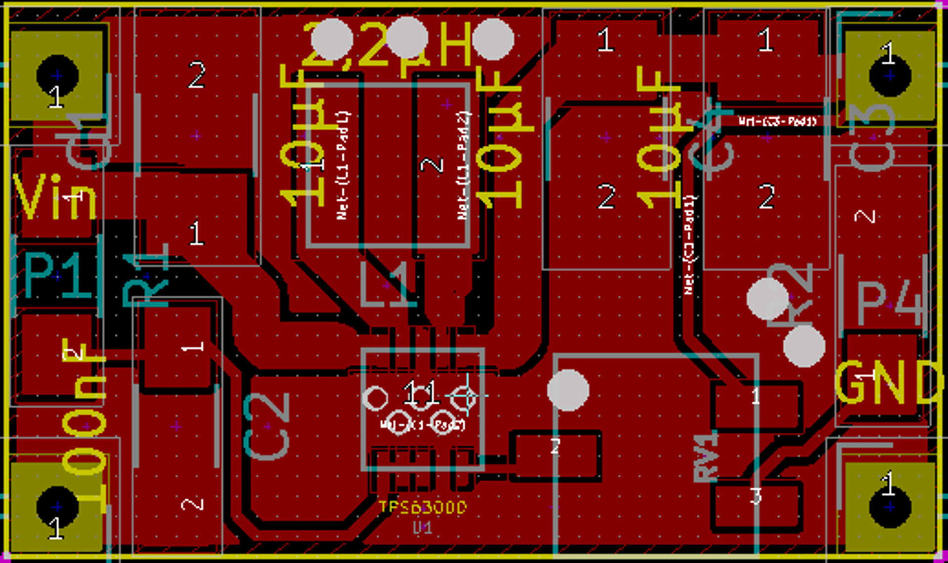
Printed circuit board developed in KiCAD. It is two-sided, the back side is a continuous layer of copper that serves as a radiator. On the platform under the heat transfer contact of the microcircuit, through holes with metallization are made to transfer heat to the back side of the board.
Picture of the board, size 14x24 mm. Of course, it could have been done two times smaller, but in this case the area of the heat sink could be insufficient. I'm just sure that when creating the board I violated all the guidelines for creating high-frequency devices:
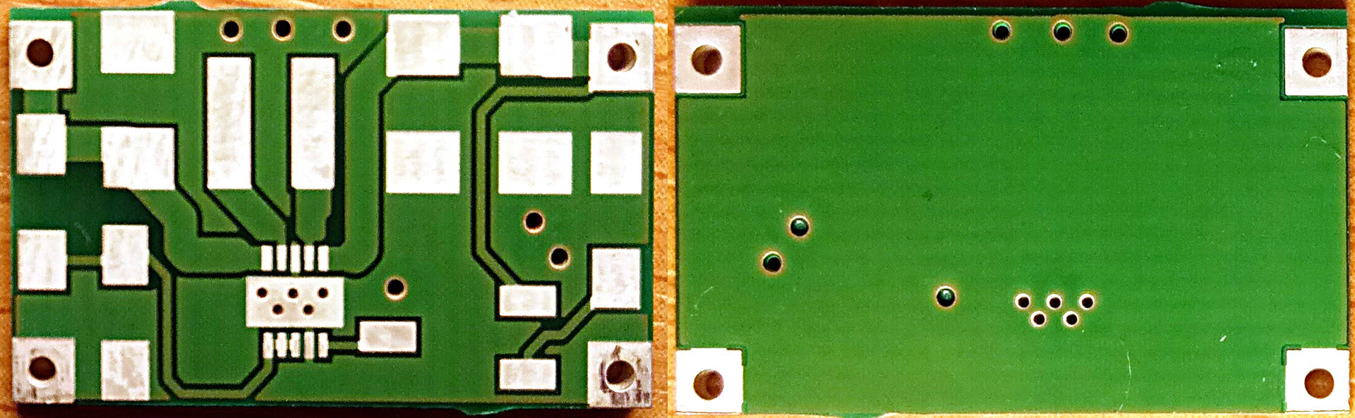
Ready copy:
The device assembly, in this photo, my rations look especially disgusting:

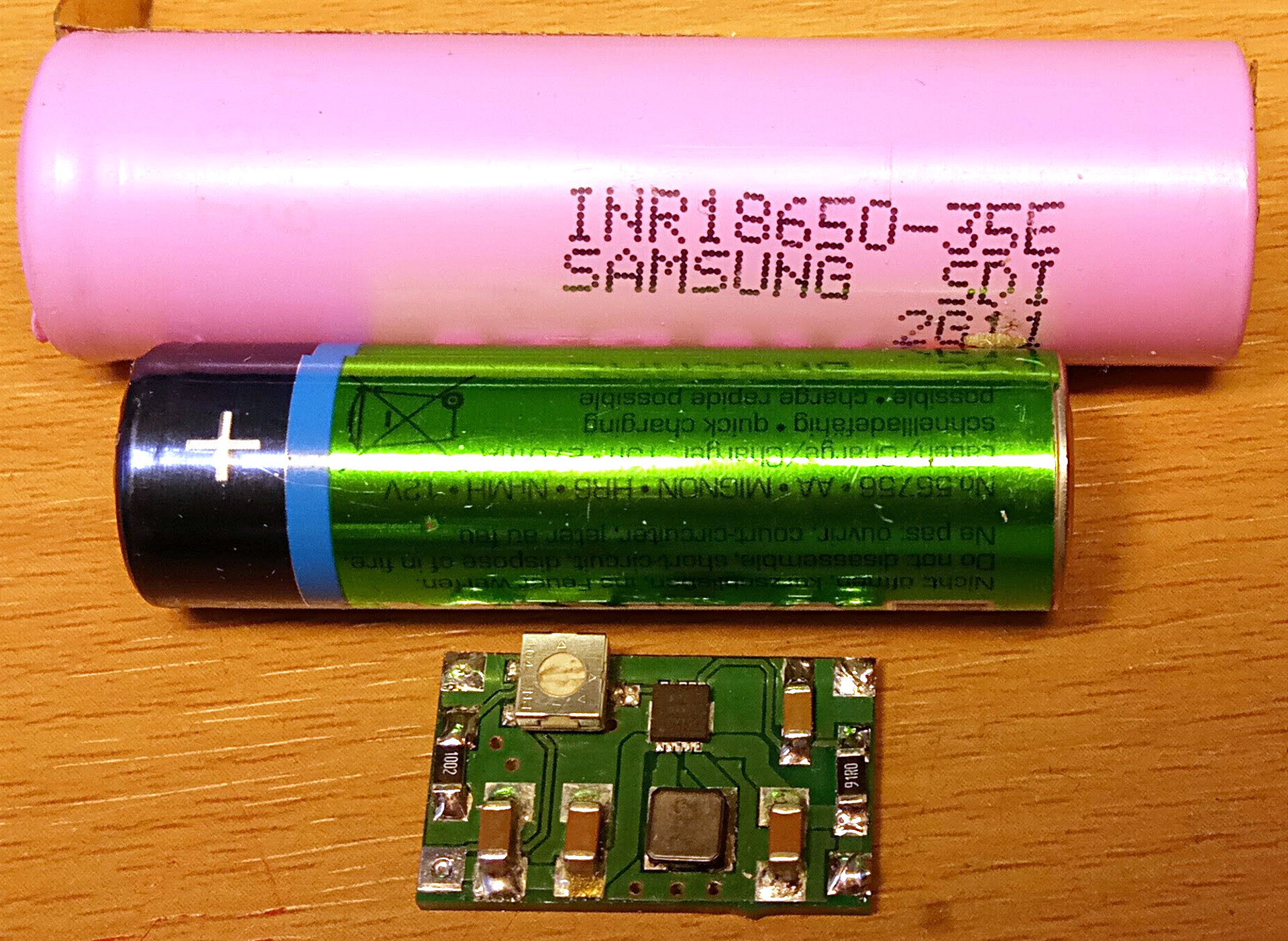
Compared with AA and 18650 batteries:
The transducer tests showed the device to be fully operational, the maximum output current at 5 V was 720 mA, i.e. about 3.6 watts. These parameters were possible only at an input voltage not lower than 2.3 V (one volt less than indicated in the technical documentation). The board at the same time heats up to 63 ° C, which is quite acceptable for the components used in the device. Adjusting the output voltage works well. No interference with the powered device and the adjacent equipment is noticed.
There is a folder with the project KiCAD.
Published under the WTFPL license.
Well, and traditional: Have fun!
Source: https://habr.com/ru/post/400617/
All Articles