Designing a switching power supply with active CMC. Episode I
Foreword
In my previous article I said that I would continue the story about working with current sensors on the Hall effect. Not a little time has passed since that moment, the continuation output has been delayed, and I am not an amateur writing a “boring theory”, so I was waiting for a practical task.
Another reason for the lack of articles was my work in one “modern successful IT-hardware-company”, now at last I left it and finally moved to freelancing, so time for the article appeared))
Recently my old mentor addressed me and just a very good person. Naturally, I could not refuse to help, but it turned out to be quite simple - I was asked to make a power supply for the FT-450 HF transceiver, which will be more stable in operation, especially with a lower input voltage than the already existing Mean Well. Please note, I’m not saying that Mean Well is a bad company, just in this case, the load is quite specific, and they have quite a good product.
')
The diagnosis is approximately as follows:
- Declared output current of 40A, in fact, when the consumption of 30-35A (in transmission) unit goes into protection;
- There is a strong heat during continuous load;
- It becomes quite bad when using it at the dacha, where the voltage in the network is 160-180V;
- The maximum voltage is 13.2-13.4V, but I would like to 13.8-14V with the ability to tweak + -20%.
A feature of this article will be that the project is moving along with it. I just sat down for him and therefore I can tell you about all the stages of development: from the TK to the finished prototype. In this format, I did not find any articles with a swoop on the geek, usually people write already having done all the work and having forgotten half the little things that often carry the main interest. I also want to write this article in an accessible language for newbies, so local gurus should be a little easier to relate to the “nonacademicism” of my syllable.
Technical requirements
Any project always begins with technical specifications and discussions. Discussions we went through, TK remains. My project is not commercial, and so to say open source, so I will not spend a lot of time and I will limit myself to the list of technical requirements.
What is it for? Those who work in companies involved in the development of something will understand me - “without a TK, the project does not take off,” but for people not connected with industrial development this moment may not be obvious. Therefore, I will explain a little ...
In the development process, if you do not rely on TK, then with a probability of about 100% you will leave from the initially desired result. For example, at first you wanted to get 1000 watts of power from the power supply, but you did not find a suitable transformer and put the one that came handy. As a result, the piece of iron became 700 W, and you were planning on 1000! For an amateur, this is not fatal, he will simply kill a lot of money and time without getting a result. For an engineer’s employer, this is a financial catastrophe, an overdue project, and for an engineer it’s often just a kick in the street. And there will be a sea of such nuances, something else will not be found past the transformer, an apple will fall on your head and you will decide to add some kind of “lightning” and so on.
How to avoid it? That is why the gloomy Soviet genius came up with "GOST 34. Development of an automated control system (ACS)" . It is enough just to do as it is necessary TK for this GOST, which will take 30-50 pages and your project at the idea stage will correspond to the end result in the form of a piece of iron, you just have to go through the points. If it says “1000 W transformer”, then you look for / extract it at 1000 W, and not at random take “a little bit less”. I worked in the military industrial complex and in private companies: the first to pray for adequate technical specifications and those. projects that usually look like a war and peace book, so our tanks are the best. The second ones are slaughtered "for the stupid damage to the forest", so civilian electronic products at the outlet in Russia in most cases are "guano on Arduin".
And so, to avoid "trash" at the exit, we will make a list of technical requirements that our prototype should have. Until he reached them - the project is considered to be incomplete. It seems simple.
Pulse Power Supply Requirements:
- Output voltage with adjustable within 10-15V DC;
- Input mains voltage: 160-255V AC;
- Secondary current: 40A
- The presence of common-mode filter;
- Availability of power factor corrector (CMC);
- Cosine fi: not less than 0.9;
- Galvanic isolation of the entrance with the exit;
- Protection against short circuit in the secondary circuit;
- Current protection response time: not more than 1 ms;
- Output voltage stability: not worse than 0.1%;
- The temperature of the power elements of the device: no more than 55 degrees at 100% load;
- The overall efficiency of the device: at least 90%;
- Availability of voltage and current indicator.
I would also like to note one feature of the designed SMPS - it is completely analog. This was quite an important requirement, since In recent years, I have mainly designed using DSP processors as a control “brain”, but this scares the “customer”. For at the moment he lives 2500 km away from me and in case of a breakdown, the repair will be delayed for a long time, therefore it is necessary to make the device with maximum maintainability. The customer is experienced in analog circuitry and will repair in case of problems without any transfers, the maximum will have to call and discuss the problem.
To summarize: when I develop, produce, and then test the SMPS and get test results that are at least as good as the ones described above, we can assume that the project is successful, the unit can be given to the owner, and be happy about another successful piece of hardware. But this is all far ahead ...
Functional diagram
I usually fought with my superiors on the topic that functional schemes for teapots and refused to draw, but since The article is still intended for beginners in electronics and for everyone to be interested in reading, I still draw it and write out what each block does. And in the absence of a full-fledged TZ, this scheme will allow me not to deviate from the original idea in the process of work.
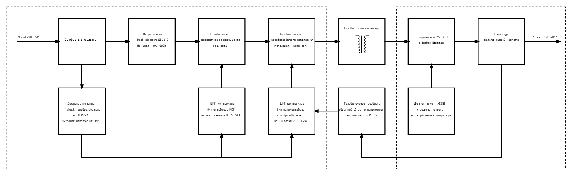
Figure 1 - Functional diagram of the SMPS
Now briefly go over each block, and in more detail these solutions will be disassembled at the design stage of circuitry. And so the modules themselves:
1) Common-mode filter - it is designed to save the network and household appliances connected to it from the interference that generates our power supply. Do not worry - any switching power supply gives them, so 90% of the SMPS has a common mode filter. He also protects our unit from interference coming from the network. I recently stumbled upon a bachelor's work on this topic, everything is quite clear there - the article . The author of the diploma Kurinkov AV, for which we thank him heartily, at least one bachelor's degree in this world will be useful))
2) The “classic” standby power supply on the TOP227 microcircuit is likely to be taken directly from the datasheet with the addition of a galvanic isolation from the network through an optocoupler. The output will be implemented as 2 windings of 15V and 1A each separated from each other. One will power the PWM controller corrector, the second PWM controller half bridge.
3) The rectifier is made on a diode bridge. Initially I wanted to apply synchronous on N-channel Mosfet, but at such voltages and at a current of 3-4 A it would be a waste of resources.
4) Active power corrector - without it, nowhere, as soon as it is a question of good efficiency, and in accordance with the requirements of the legislation, the use of CMC is mandatory. KKM is in fact an ordinary booster converter, which will close 2 problems: low input voltage, since at its output, it will consistently produce 380V and will allow it to evenly draw power from the network. The chip used a very popular, the Chinese (and not only) like to put it in the welding inverter for the same purposes - ICE2PCS01 . I won't conceal it - I took it as a time-tested solution, I collected 6 KVA CMC for a semi-automatic machine on it and there are no problems for more than a year, reliability bribes me.
5) Directly voltage converter is implemented in topology - “half bridge”, I advise you to read the chapter in the book by Semenov “Power electronics: from simple to complex” to get acquainted with it. The half-bridge controller is implemented on a “classic”
6) I plan to implement a power transformer on Epcos core of the type ETD44 / 22/15 from material N95. Perhaps my choice will change further when I will calculate hank data and overall power.
7) For a long time hesitated between the choice of type of rectifier on the secondary winding between the dual Schottky diode and the synchronous rectifier. You can put a dual Schottky diode, but this is P = 0.6V * 40A = 24 W to heat, with a small output power of about 650 W, a loss of 4% is obtained! When using the most common IRF3205 in a synchronous rectifier with the resistance of the heat channel, P = 0.008 Ohm * 40A * 40A = 12.8 W will stand out. It turns out we win 2 times or 2% efficiency! Everything was beautiful until I assembled a solution on the IR11688S on the layout . Dynamic losses for switching were added to the static losses on the channel, as a result, that was exactly what happened. The capacity of field vehicles for large currents is still large. This is treated by drivers like HCPL3120, but this is an increase in the price of the product and an excessive complication of the circuit design. Actually from these considerations, it was decided to put the double Schottky and sleep peacefully.
8) The LC circuit at the output, firstly, will reduce the ripple current, and secondly, will allow to “cut off” all harmonics. The latter problem is extremely relevant when powering devices operating in the radio frequency range and incorporating high-frequency analog circuits. We are talking about the HF transceiver, so here the filter is simply vital, otherwise the interference will "climb through" on the air. In ideals, you can still put a linear stabilizer on the output and get minimal pulsations in units of mV, but in fact, the OS speed will allow you to get voltage pulsations within 20-30 mV without a “reboiler”, the critical nodes are powered inside the transceiver through their LDOs, so its redundancy is obvious.
Well, we ran through the functional and this is just the beginning)) But nothing, it will continue to be more cheerful because the most interesting part begins - the calculations of everything and everything!
Calculation of power transformer for half-bridge voltage converter
Now it’s worth a little to think about constructive and topology. I plan to use field-effect transistors, not IGBTs, so the working frequency can be chosen more, while thinking about 100 or 125 kHz, the same frequency will be on the CMC by the way. Increasing the frequency will reduce the size of the transformer. On the other hand, I do not want to pick up the frequency very much, because I use TL494 as a controller, after 150 kHz it shows itself not so well, and the dynamic losses will increase.
Proceeding from such input, we will count our transformer. I have several sets of ETD44 / 22/15 available and therefore, while I am guided by it, the list of initial data is as follows:
1) Material N95;
2) Core type ETD44 / 22/15;
3) Operating frequency - 100 kHz;
4) Output voltage - 15V;
5) Output current - 40A.
For the calculations of transformers up to 5 kW using the program "Old Man", it is convenient and quite accurately considers. After 5 kW magic begins, the frequencies grow to reduce the size, and the field and current densities reach such values that even the skin effect is able to change the parameters almost 2 times, therefore for large powers I use the old-fashioned method “with formulas and output with a pencil on paper. " Entering into the program its input data the following result was obtained:
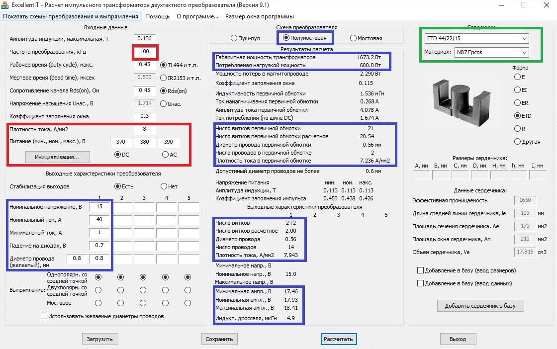
Figure 2 - The result of the calculation of the transformer for half bridge
The figure on the left side is marked with input data, I described them above. In the center, in purple, the results that interest us most of all are highlighted ; I will briefly go over them:
1) The input voltage is 380V DC, it is stabilized, because half bridge eats with KKM. This power simplifies the design of many nodes, because ripple currents are minimal and the transformer does not have to pull the voltage at the input mains voltage 140V.
2) The power consumed (pumped through the core) turned out to be 600 W, which is 2 times less overall (that which the core can pump without being saturated) power, which means everything is good. I didn’t find the material N95 in the program, but on the Epcos website in the datasheet I saw that the N87 and N95 would give very similar results, checking on a piece of paper that I found out that the difference of 50 watts of overall power is not a terrible error.
3) Data on the primary winding: 21 turns we wind in 2 wires with a diameter of 0.8 mm, I think everything is clear here? The current density is about 8A / mm2, which means that the windings will not overheat - all is well.
4) Data on the secondary winding: we wind 2 windings with 2 turns in each wire, also 0.8 mm, but already at 14 - all the same, the current is 40A! Next, we connect the beginning of one winding and the end of another, as I will explain further, for some reason, often people assemble into this stupor at this moment. There is no magic either.
5) The inductance of the output choke is 4.9 μH, the current, respectively, 40A. We need it, so that at the output of our unit there is no huge ripple current, in the process of debugging I will show on the oscilloscope work with it and without it, everything will become clear.
The calculation took 5 minutes, if someone has questions, then in the comments or drugs ask - I will. In order not to look for the program itself, I suggest downloading it from the cloud by the link . And my great thanks to the old man for his work!
The next logical step will be to calculate the output choke for the half bridge, this is exactly the one that is 4.9 μH.
Calculation of winding parameters for the output choke
The input data we received in the previous paragraph when calculating the transformer is:
1) Inductance - 4.9 μH;
2) Rated current - 40A;
3) Amplitude in front of the choke - 18V;
4) The voltage after the choke is 15V.
Use the same program from the old man (they are all in the link above) and get the following data:
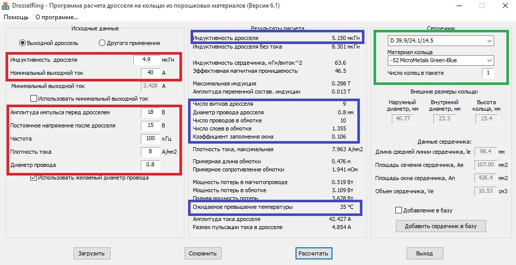
Figure 3 - Calculated data for winding the output choke
Now let's go over the results:
1) According to the input data, there are 2 nuances: the frequency is chosen the same, on which the converter works, I think this is logical. The second point is related to the current density, I note right away - the throttle should be heated ! That's just how much we already determine, I chose a current density of 8A / mm 2 to get a temperature of 35 degrees, which is visible in the output (marked in green). After all, as we remember according to the requirements of the output, we need a “cold IIP”. Just want to note for beginners maybe not quite the obvious point - the choke will warm less, if a large current flows through it, that is, at a nominal load of 40A, the choke will have a minimum heat. When the current is less than the rated current, for a part of the energy it starts working as a resistive load (resistor) and turns all the excess energy into heat;
2) The maximum induction, this value can not be exceeded, otherwise the magnetic field will saturate the core and everything will be very bad. This parameter depends on the material and its dimensions. For modern sputtered iron cores, a typical value is 0.5-0.55 T;
3) Winding data: 9 turns are wound with an oblique of 10 cores with a diameter of 0.8 mm. The program even approximately indicates how many layers are needed for this. I will wind in 9 lived, because then it will be convenient to divide the big braid into 3 "pigtails" with 3 cores each and without any problems to unsolder them on the board;
4) Actually the ring itself on which I will wind has dimensions - 40/24/14.5 mm, it is enough with a margin. Material number 52, I think many have seen in the ATC blocks yellow-blue color rings, they are often used in group stabilization chokes (DGS).
Calculation of the transformer on duty power supply
The functional diagram shows that I want to use the “classic” flayback on TOP227 as an on-duty power supply unit, all PWM controllers, indications and cooling fans will be powered from it. The fact that the fans will be powered from the duty rooms, I realized only after some time, so this moment is not displayed on the diagram, but nothing is the same real-time development))
Let's adjust our input data a bit, what we need:
1) Output windings for PWM: 15V 1A + 15V 1A;
2) Self-powered output winding: 15V 0.1A;
3) Output winding for cooling: 15V 1A.
We get the need for a power supply with a total power of 2 * 15W + 1.5W + 15W = 46.5 W. This is the normal power for TOP227, I use it in small SMEs up to 75 W for all sorts of batteries, screwdrivers and other junk, for many years
We go to another program of the Old Man and consider the transformer for flayback:
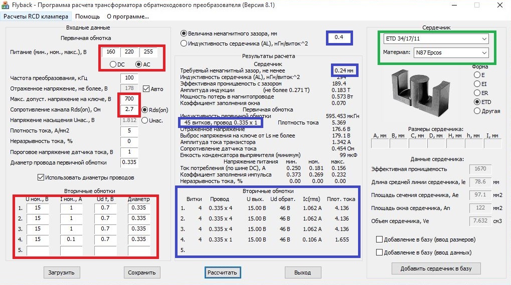
Figure 4 - Calculated data for standby power transformer
1) The choice of the core is justified simply - I have it in the amount of the box and the very 75 watts it pulls)) The data on the core is here . It is made of material N87 and has a gap of 0.2 mm in each half or 0.4 mm, the so-called full gap. This core is directly intended for chokes, and for flyback converters, this inductance is the choke, but I will not get into the jungle so far.If there was no gap in the half-bridge transformer, it is mandatory for the flyback converter, otherwise, like any choke, it simply goes into saturation without a gap.
2) Data on the 700V “drain-source” key and 2.7 ohm channel resistance are taken from the datasheet on TOP227, this controller has a power switch built into the microcircuit itself.
3) The input voltage took the minimum with a margin of 160V, this is done so that in case of switching off the power supply itself, there is a duty room and an indication in the work, they will report an abnormally low supply voltage.
4) Our primary winding consists of 45 turns with a wire of 0.335 mm in one core. The secondary windings are 4 turns and 4 cores with a wire of 0.335 mm (diameter), the self-power winding has the same parameters, so everything is the same, only 1 core, because the current is much lower.
Calculation of the power throttle active power corrector
I think the most interesting part of this project is the power factor corrector, since there is little information on them on the Internet, and there are even fewer working and described schemes.
We select the program for the calculation - PFC_ring (PFC is KCM-like bass mode), we use the following
inputs : 1) Input power supply voltage - 140 - 265V;
2) Rated power - 600 W;
3) Output voltage - 380V DC;
4) Working frequency - 100 kHz, due to the choice of PWM controller. Figure 5 - Calculation of the power choke of an active CMC 1) On the left, as usual, enter the initial data, setting 140V as the minimum threshold we get a unit that can operate with a voltage of 140V, so we get the “built-in voltage regulator”;
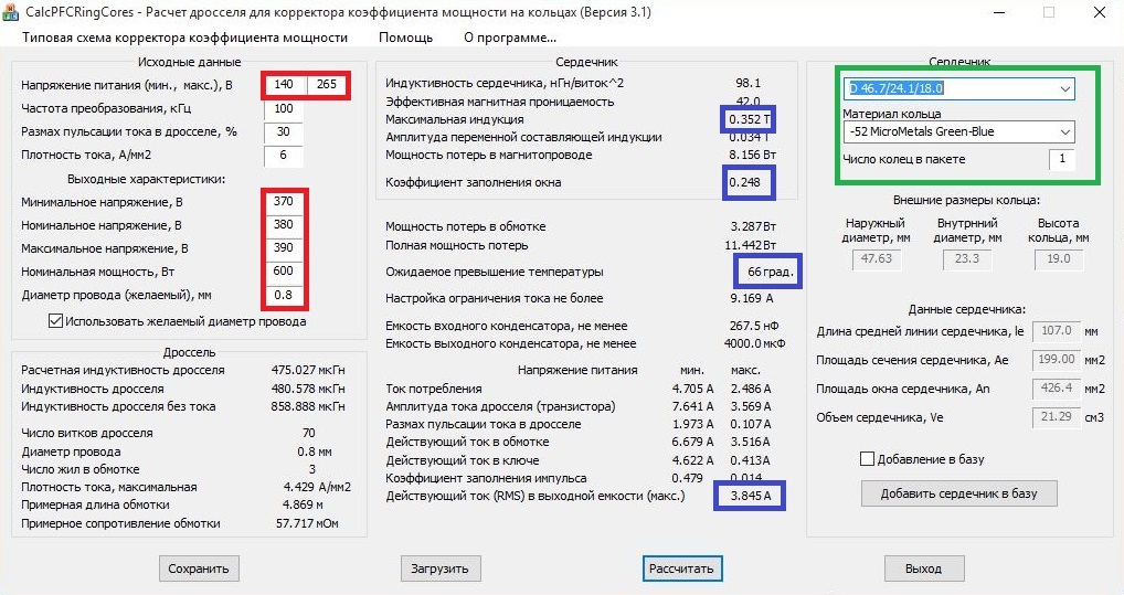
2) The core chose - 46 / 24/18 . According to the calculations, it also got on the ring with a diameter of 39 mm, but it turned out 110 turns - it would be difficult to wind into a heap of layers, and the reserve by induction in the CMC is very helpful, eventually it gets 0.35 T at a tolerable 0.5 T;
3) Many are frightened by the following inscription: “Capacity of the output capacitor” 4000 uF! Those who are in the subject will be horrified by such a figure, these are 15 huge and expensive Conders (300-350r / pcs), but do not be alarmed - this figure is useless for us and it is impossible to be guided by it, the Old man probably in the calculations or an extra zero somewhere added or we are talking about capacitors to huge ESRs and we need to parallelize 15 pieces. For us, there is a more literate parameter - "Actual current in the output capacitance" 3.845A. 1 good electrolyte from Epcos with its low internal ESR is able to give 3-4A. I will be safe and put 2 pieces in parallel to reduce the ESR and get a minimum of 6A from the legs of the conder.
Circuitry active power factor corrector and input circuits
That came to the right to the most interesting point - circuitry. I will begin, of course, in order: from the entrance to the exit. I think those who disassembled any switching power supply saw a cluster of capacitors (usually blue) and a choke right next to the input cable connection connector, this module is called the common mode filter.
What is common-mode noise and why you can fight them without any problems, I’ll only briefly explain. Common mode interferences are all interferences that travel between current conductors and ground. They come to us from the power network, and our power supply also radiates them in a certain form in order to get rid of them - we put the filter.
The method of calculation is in many sources, I also advise you to look at the books of Semenov: the first (3.3) and the second (3.2). I prefer the tasks related to EMR to be modeled in CST Suite Studio and using the “selection method” to get the most optimal parameters. In addition, this filter, unlike the low-frequency LC filter, does not require high accuracy, so for 90% of the SMPS, you can use the data given in my schematics.
To control the CMC I decided to use the IC - ICE2PCS01GXUMA1 . It allows you to build a fairly simple and reliable converter, as already written ACKM - this is nothing more than a booster. Figure 6 - Diagram of the input circuits and active CMC
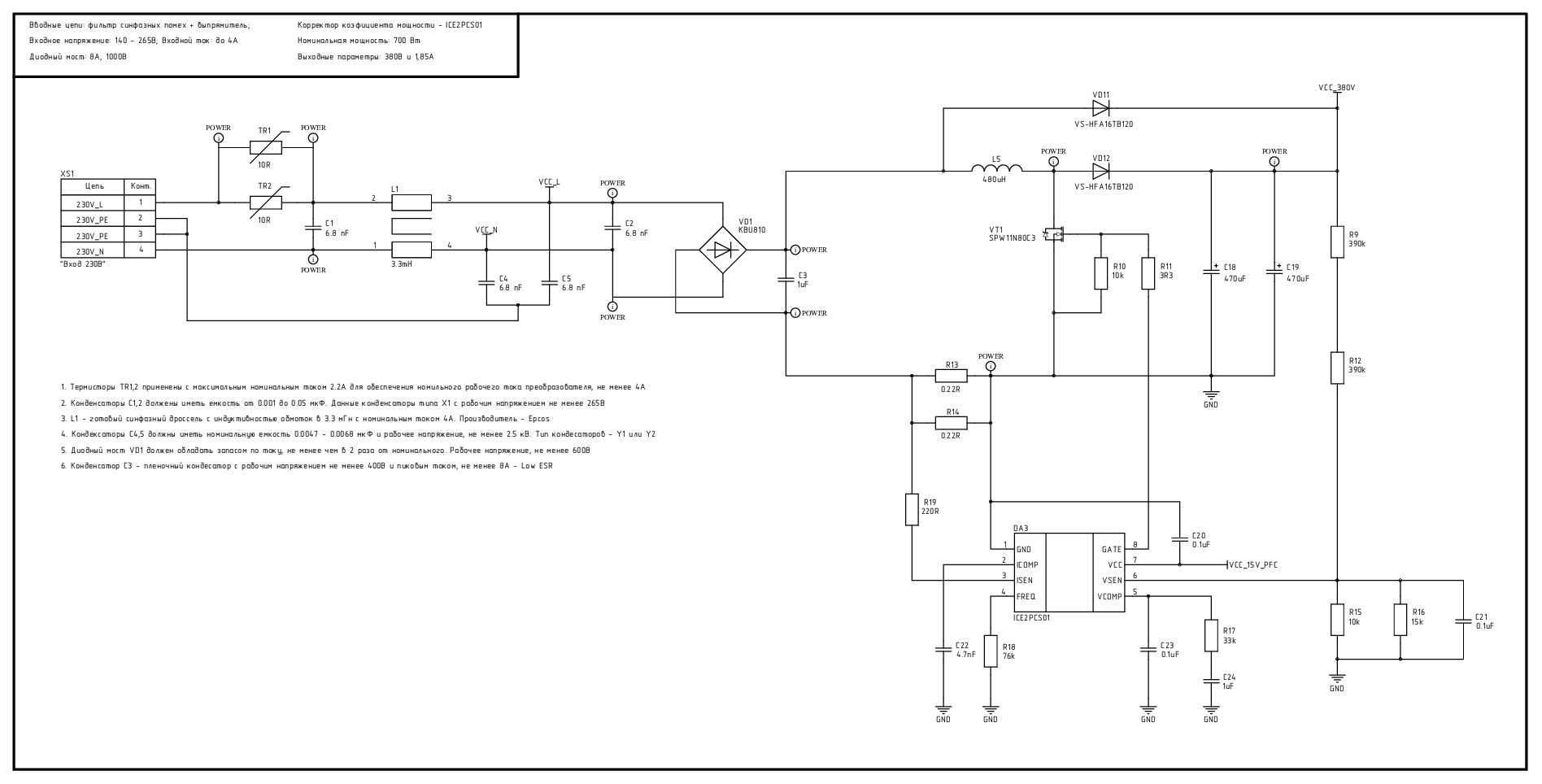
It is a little about circuit engineering ... In the modern world it is difficult to invent something - it is a fact. You can make a cool piece of iron, but with a probability of 99.99%, someone has already done it, but maybe just in a worse performance. All of this applies to electronics, you can sit for months and invent schemes and in the end it turns out that it was invented 10 years ago. This is by no means a reason to stop reinventing! This is just a reason to look for better information. I use the chip, which produces a giant industry - Infineon Technologies . Therefore, with a high probability, they provided for a certain debug board for their controller, so I immediately went to digikey.com , where I usually purchase, and hammered in the name of my stone - in addition to being able to buy a search engine microchip on the website, I issued one debugging (Evaluation Board ) - EVALPFC2-ICE2PCS01 . Buy it is no longer possible, only from the manufacturer under the order, but I do not need. But there is documentation on a ready-made working solution with an open scheme, trace of the board and a list of components! Here it is a ready-made solution, nothing needs to be invented, the manufacturer has done everything to buy his products, and for developers almost always the availability of documentation comes first in the requirements for the elements and only then the price. There is only one “BUT” - a 300W debugging board, and I need 700, but not terrible - the architecture itself is already 90% of work, I recalculate the nominal values for 15 minutes, and so we went:
1) I recalculated the power choke L5 and the data for its windings are shown in Figure 5. We have obtained that instead of an inductance of 1240 μH, a value of 480 μH will be needed, although the value of the current has increased 2.5 times;
2) Diodes VD11,12 must be at least the output voltage, that is, 400V and above, and must also withstand the pulse value of the current in the device. Another important parameter is the reverse recovery time, since my corrector works at a frequency of 100 kHz and a normal diode just won't keep up. For this task suitable pulsed or ultrafast diodes. I applied VS-HFA16TB120-N3 to 1200V and 16A diodes with a recovery time of only 30 µs, since They correspond to all parameters, are produced in a TO-220-2 package, convenient for cooling, and are not expensive at about $ 2-2.5;
3) The VT1 transistor must be at least 1.5 times the drain-source voltage margin and withstand the pulse current value (x2 of the nominal). Considering the frequency, it is better to use the N-channel Mosfet, especially in the last couple of years they have become very affordable. I applied the key to 800V, because emissions can reach 1.5y amplitude (about 550V) and there is no additional margin. The current of this key is 11A and that it is important it is manufactured in the TO-247 package, which means it is very easy to cool and isolate it from the radiator;
4) Output capacitors C18,19 are an important node, since we have a single-ended converter, and it is they who smooth the current pulsations. The capacitor should be preferably 450V in order to have a voltage margin and is capable of delivering up to 8A of current at peak loads. In the spoiler above, I wrote about capacitors, a good electrolyte is capable of delivering 3-4A of instantaneous current and it is limited solely to the ESR of the capacitor. To get the necessary 8A, I decided to reduce the ESR due to the parallel connection of 2 capacitors, each by 470 uF and 450V. Such a "battery" is able to give 11A, because applied condensers rather good from Epcos from the Low ESR line;
5) Another thing is to recalculate the current sensor in the form of a shunt, in the datasheet this topic is fully disclosed as a whole section.
Knot on-duty power supply IIP
A bit of galvanic isolation, the decision I have here is a bit peculiar, I will explain why it is not otherwise:
1) “Primary cell and secondary market are untied” - made so that in case of breakdown TOP227 “brains” would not burn and repair would be limited only to replacement of the microcircuit itself ;
2) "Secondary windings are not untied with each other" - and why? I have all the control modules combined with common ground. Of course, you can be puzzled and unleash the "brains" of the CCM, half-bridge and indication, but this is relevant when the price of the control circuits is very high and makes up 20-30% of the cost of the device itself. This happens if I use DSP or some MK motor control for control, but in my case TL for 15 rubles and IR2110 do not cost such costs as optical isolation or isolation on transformers - the complexity of this solution will greatly increase along with the price tag;
3) “If secondary cells are galvanically connected, then why make them as many as 3 pieces when you can make 1 piece per 3A?” -
Now the circuitry itself, as I expected, was not particularly removed from the datasheet on TOP227, added chokes on secondary windings from “frills” in order to reduce current ripple, an LED display was added to each channel. Snubber applied the RC shny, because for some reason, the suppressor did not keep up with the emissions, although it should. Yes, and I am not a supporter of the use of suppressors, well, I don’t like them just after having been tortured with them a couple of times. Another “stone in their garden” does not work at a high frequency, the modern base allows designing flyback converters at frequencies of 1-1.5 MHz and there they are needed like a goat button accordion.
One more thing - I took the power for the duty room after the in-phase filter, but before the diode bridge. Yes, I had to put another diode bridge for $ 0.2, but then I saved about $ 3 for one more phase locker - profit! Figure 7 - Diagram of the on-duty power supply for the control circuit of the IIP I mentioned that I first write this article for beginners and those who want to know the Jedi power of circuitry, so I’ll show you where the ratings of all the components in this module come from, because we often open the datasheet that not all components can be calculated by the available formulas, since manufacturers make documentation for trained engineers, not beginners and amateurs - oh, this cruel world! 1) VD4 - its voltage must be not less than: U M
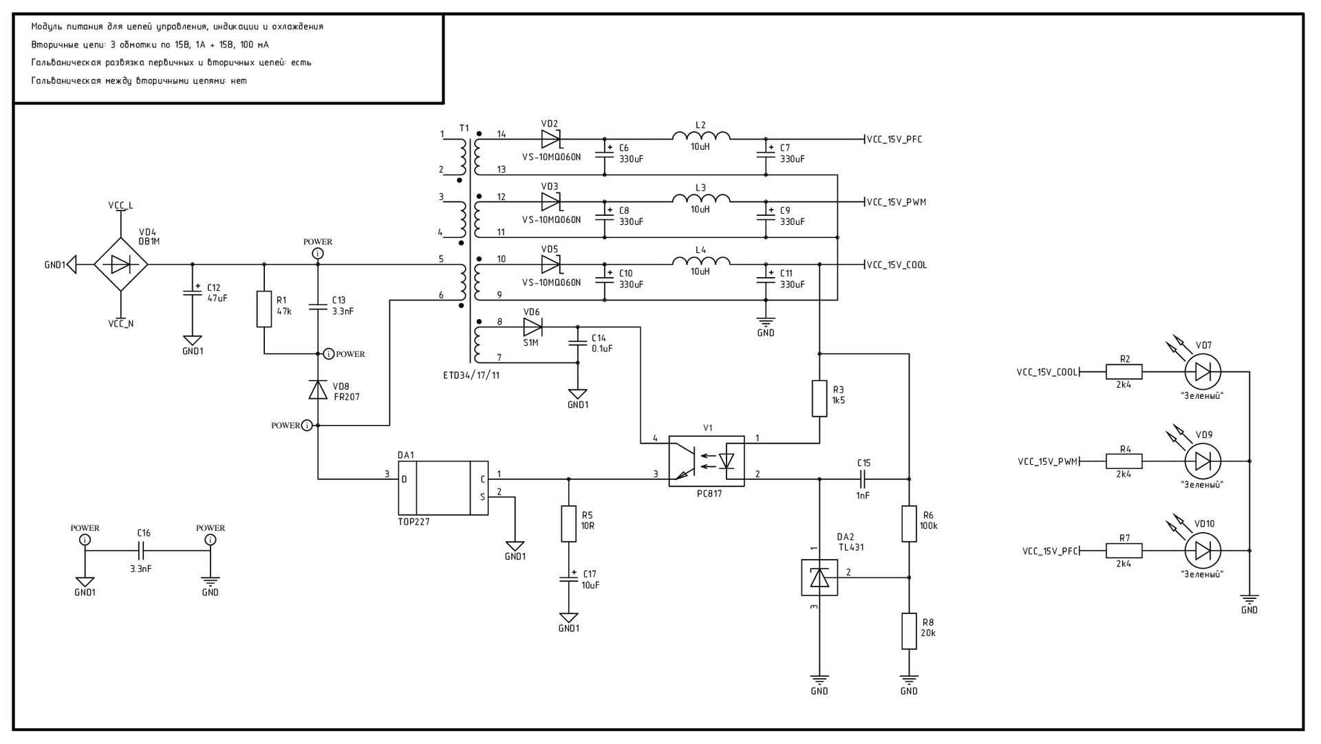
= 265V * 1.41 = 374V . Where did these numbers come from: "265V" - the maximum voltage of the SMPS is 255V and 10V to the reserve, "1.41" is a factor that recalculate the alternating voltage up to the diode bridge into the DC voltage after it.
Rated current not less: I = P / (µ * U BX ) = (15V * 1A * 3 + 15V * 0.1A) / (140V * 0.85) = 0.39A. It is better to take at least with a double margin, because at the moment of switching on the capacitor will be charged and the current peak will be rather large. Now in numbers: “15V and 1A” are our windings, “140V” is the minimum voltage at the input of our power supply unit. Why minimum? And because in this case there will be a maximum current - the worst conditions must always be considered so that nothing explodes. "0.85" is the efficiency of our converter, as practice shows, this is the average value for this chip, and it is even specified in the datasheet.
2) R1 and C13 - are considered in the Old Man program in the same place as the transformer, in the upper left corner of the “RCD snubber”.
3) VD8 - taken on the basis of considerations that the maximum voltage is not less than that of the power key built into the chip, in my case it is not less than 700V. The current is not less than the current consumption of the circuit, that is, the requirements for the diode:> 700V and> 0.4A, with FR207 values of 1000V and 2A - everything fits.
4) VD2,3,5,6 - these must be Schottky diodes or pulsed diodes. Schottky is preferable due to the lower voltage drop, although at such currents it is not critical. Also in the transformer calculation table ( Figure 4) there is an indicator "reverse voltage", I have it 46V - it means the voltage of the diodes must be at least 46V. The closest Schottky 60V is perfect for this task. The current of the diode is not less than the nominal, although there is one subtlety - the load will be pulsed: the current is nominal 1A, but the consumption can theoretically be higher up to 2A just briefly when the key is charged. Therefore, I took Schottky on 60V and 2A - the stock of ass does not shake as they say in our valiant army.
5) C6-C11 - the minimum capacitance of the output capacitor is shown in Figure 4, in single-ended converters it is this that reduces the ripple of the current, giving off energy. I got 99 microfarads - it will actually work, but the pulsations will be about 1-2V. This is again an experience, or considered hands. In order not to spoil the paper, you can simulate the output circuit in MicroCap. I set a total capacity of 660 microfarad, this is more than enough to produce pulsations within 100 mV.
6) L2-L4 - inductances are also modeled in MicroCap, the easiest way and accurate. And so you can put with an inductance from 2.2 to 10 μH without any fear, will work with dignity. The choke current must not be less than the nominal, that is, 1A. I used chokes with an inductance of 10 μH and a current of 1.1 A from Epcos.
7) R3 - everything is according to Ohm's law: R = (U P - U D ) / I C = (15.3 V - 2.6 V) / 0.008 A = 1570 Ohms - the closest nominal 1.5 kOhm. "15.3V" is the output voltage from which the LED of the optocoupler is powered. "2.6V" - a drop on the LED (taken in datasheet). "0.008A or 8 mA" - the current that we send to the optocoupler can be up to 20 mA, but it makes no sense and 1-10 mA is enough - it will live longer.
8) R6 and R8 - form a voltage divider, which actually sets the output voltage. It is calculated as follows: U OUT = U REF * (1 + R2 / R8) = 2.56 V * (1 + 100/20) = 2.56 V * 6 = 15.36 V - great! "U REF= 2.56V ”is the voltage at which the TL431“ programmable zener diode ”punches, that is, when the voltage reaches 2.56V on the control leg 2, the zener diode opens and delivers the“ ground ”from leg 3 to leg 1 and, accordingly, to the anode of the LED of the optocoupler. So TOP227 learns that enough is enough to pump energy. The values of the resistors themselves are chosen so that when the output voltage is divided (which we want), it turns out to be exactly 2.56V.
9) R2, R4, R7 - current-limiting resistors on LEDs, I do not want to shine them in full heat, so I will not give 12-15 mA, which they want on datasheet, but only 5 mA, otherwise they are not blind so badly. Again we resort to Ohm’s law: R = (U P - U D ) / I C = (15.3 V - 2.6 V) / 0.005 A = 2540 Ohm - the nearest nominal 2.4 kOhm.
«»
The task of this module is to convert the voltage from the CMC with a nominal value of 380V to the required output 15V. I chose the half-bridge based on the reduced number of components on the background of a full bridge, as well as a rather high efficiency value. I did not bother with the resonance, the dimensions are not critical for me, and a gain of 1-2% is not worth the effort.
The device is built according to a common scheme: "PWM controller (TL494) + half bridge driver (IR2110S) + 2 x N-channel Mosfet-ah + Schottky diode in the output rectifier", so there is nothing supernova here, I only added current protection on Hollovsky current sensor ACS758, because the current is large enough and I want to measure it as precisely as possible - the equipment will be more whole. Figure 8 - Diagram of the half-bridge voltage converter

Now I’ll go over the components so that the reader, who wants to repeat this device, understands where it comes from and how to recalculate the nominal values for its own task :
1) One of the main parameters for the PWM controller is the frequency of the built-in generator. The operating frequency for a push-pull power supply will be 1/2 of the generator frequency. This parameter is set using the RC-chain, on the diagram it is R37-C43. The formula for calculating the generator frequency is given in the datasheet and looks like this: f osc = 1.1 / (R T * C T ) . I have a working frequency of 100 kHz, which means that the calculated frequency for the generator should be twice as high - 200 kHz. Consider: let C43 has a capacity of 2.2 nF, thenR T = 1.1 / (200 000 Hz * 0.0000022 F) = 2500 Ohm - I take the nearest nominal 2.4 kΩ;
2) The current feedback is implemented on the built-in comparator in the PWM controller. At a current of 40A according to datasheet ACS758-50B voltage is: U OUT = U VCC + I MOD * 0,04V / A = (5V / 2) + (40A * 0,04V / A) = 2.5V + 1.6V = 4.1V . In order for the comparator to generate an error in the saw log.1 and the PWM controller understood that it is time to reduce the PWM duty cycle, the signal from the sensor must be sent to the positive input of the OU, and the inverse voltage must be supplied with the reference voltage 4.1V. TL494 has a built-in reference voltage source (ION) of 5V, it is necessary to make a voltage divider with a coefficient. division equal to:5V / 4.1V = 1.22 . This divider is implemented on the R27-R26, I picked up the denominations of 2 and 10 kΩ, coefficient. division will be equal to 1.2V and on the inverse of the comparator input there will be a reference voltage equal to: U OP = U REF / (1 + R27 / R26) = 5V / (1 + 2/10) = 4.16V - this value corresponds to the current in 41.3A. So leave;
3) Voltage feedback “classic” will not talk much about it. The output voltage through the divider is fed to the TL431 with an opening voltage of 2.56V. As soon as the voltage reaches the desired value, the TL431 connects the LED of the optocoupler to the ground and it lights up, supplying + 5V to the positive input of the embedded op amp (there are already 2 of them in the TL494). When the optocoupler is closed the input through the resistor R30 is pulled to the ground and the comparator outputs a log.0. 1/2 U REF equal to 2.5V is fed to the inverse input through the divider ; therefore, when the optocoupler is closed on the direct input 0V and the output of the op-amp is 0, when the optocoupler is open, the direct input 5V is greater than 2.5V and the output of the op-amp is 1, reporting an error;
4) C25, 26 - capacitors create a "midpoint", capacitors are used with an operating voltage of 200-250V. I put Epcos capacitors at 220 uF and 250V;
5) VT2, 3 - field-effect transistors, the same as in CMC. The drain-source voltage with a large margin, in fact, there will not be more than 200V + emissions of 50-100V. This stock allows you to abandon snubber chains. The current in the keys will be: I VT = P OUT / U DEL = 600 W / (380V / 2) = 600 W / 190V = 3.15A . Our keys are 11A, so even peak short-term overloads will not damage the converter;
6) We have already calculated the output choke L6 and the results are shown in Figure 3 .
The circuitry of the power unit and the control are fairly standard, if you suddenly have questions, feel free to ask in the comments or in personal messages. If possible, I will try to answer and explain to everyone.
PCB design of switching power supply
So I got to the stage, which remains for many something sacred - design / development / tracing of the PCB. Why do I prefer the term "design"? It is closer to the essence of this operation, for me “wiring” the board is always a creative process, like an artist, writing a picture, and it will be easier for people from other countries to understand what you are doing.
The board design process itself does not contain any pitfalls, they are contained in the device for which it is intended. In fact, power electronics does not put forward some wild number of rules and requirements against the background of the same microwave analogue or high-speed digital data buses.
I will list the main requirements and rules concerning power circuitry, it will allow to implement 99% of amateur designs. I will not tell about the nuances and “tricks” - everyone should fill in his own cones, get experience and operate on them. And so it went:
1) Width of conductors - the wider they are, the better. There are several reasons for this. First, by increasing this parameter, we reduce the parasitic inductance of the conductors, which means that there will be less interference, interference and other bad things in the control signal. Secondly, we can pass more current, because the conductor section will be larger. Thirdly, by increasing the surface area of the conductor, we increase the amount of heat and the intensity with which it is given, and therefore it is much easier to cool such conductors and we can afford a large current density;
A little about current density in printed conductors
Often people do not think about this parameter and I had to meet where the power section was made with 0.6 mm conductors with 80% of the board area just empty. Why do so for me personally a mystery.
So what is the current density that can be taken into account? For a conventional wire, the standard figure is 10A / mm 2 , this limitation is tied to the cooling of the wire. You can skip more current, but before that, lower it into liquid nitrogen. In flat conductors, like on a printed circuit board for example, the surface area is large, it is easier to cool them, which means you can afford large current densities. For normal conditions with passive or air cooling, it is customary to take into account 35-50 A / mm 2 , where 35 is for passive cooling, 50 is in the presence of artificial air circulation (my case). There is one more figure - 125 A / mm 2 , this is a really big figure, not all superconductors can afford it, but it is achievable only with immersion liquid cooling.
I ran into the latter when working with one company engaged in engineering communications and server design. My part was just the design of the motherboard, namely the part with multiphase power and switching. I was very surprised when I saw a current density of 125 A / mm 2 , but they explained to me and showed such an opportunity on the stand - then I understood why the whole racks with servers are immersed in huge oil pools)))
In my piece of iron, everything is simpler, 50 A / mm 2 is quite an adequate figure, with a copper thickness of 35 μm, the polygons without problems provide the desired cross section. The rest was for general development and understanding of the issue.
2) Length of conductors - in this paragraph there is no need to equalize the lines with an accuracy of 0.1 mm as it is done, for example, when wiring the DDR3 data bus. Although it is still highly desirable to make the length of the signal lines approximately equal to the length. It will be enough for + -30% of the length, the main thing is not to do HIN 10 times longer than LIN. It is necessary that the signal fronts do not move relative to each other, because even at a frequency of just a hundred kilohertz, a difference of 5-10 times can cause a through current in the keys. This is especially true with a small value of "dead time", even with 3% in TL494 this is important;
3) The gap between the conductors - it is necessary to reduce leakage currents, especially for conductors, where the RF signal (PWM) flows, because the field in the conductors occurs strongly and the RF signal due to the skin effect tends to break out both on the surface of the conductor and beyond his limits. A gap of 2-3 mm is usually sufficient;
4) The isolation gap is the gap between the galvanically isolated sections of the board, usually the requirement for a breakdown of about 5 kV. To break through 1 mm of air, we need about 1-1.2 kV, but in our country, breakdown is possible not only by air, but also by textolite and mask. In the factory used materials passing electrical testing and you can sleep peacefully. Therefore, the main problem is the air and from the above described conditions it can be concluded that about 5-6 mm of gap will suffice. Basically, the separation of landfills under the transformer, because It is the primary means of galvanic isolation.
Now let's proceed directly to the design of the board, I will not in this article tell you super in detail, and generally not write a whole book of the text of the desire. If there is a large group of people willing (at the end I’ll do a survey), then I’ll just take videos on the “wiring” of this device, it will be faster and more informative.
Stages of the PCB creation:
1) The first step is to determine the approximate dimensions of the device. If you have a ready-made case, then you should measure the seat in it and build on the size of the board from it. I plan to make the case to order from aluminum or brass, so I will try to make the most compact device without loss of quality and performance characteristics.
Figure 9 - Creating a Future Procurement
Remember - board dimensions must be multiples of 1 mm! Or at least 0.5 mm, otherwise you still remember my testament of
PS thanks comrade. Lunkov because he still conveyed to me this bright thought))
Here I did 4 operations:
a) Made the board itself with dimensions of 250x150 mm. While this is an approximate size, then I think it will shrink noticeably;
b) rounded the corners; in the process of delivery and assembly, the sharp ones will be killed and crumple + the board looks nicer;
c) Placed mounting holes, not metallized, with a hole diameter of 3 mm for standard fasteners and racks;
d) Created the “NPTH” class, into which I identified all non-metallized holes and created for it a rule creating a gap of 0.4 mm between all other components and components of the class. This is the technological requirement of "Resonit" for the standard accuracy class (4th).
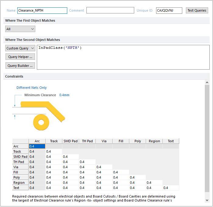
Figure 10 - Creating a rule for non-metallized holes
2) The next step is to make the arrangement of components with all the requirements, it should already be very close to the final version, because more parts are now determined by the final dimensions of the board and its form factor.
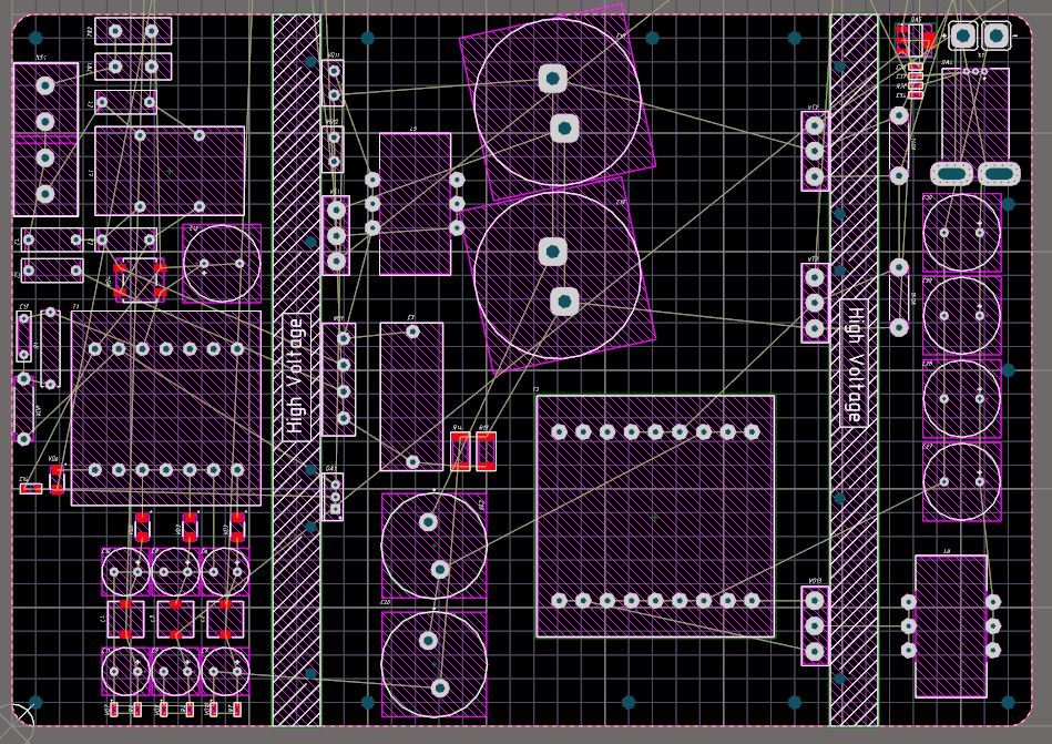
Figure 11 - The primary placement of components
Installed the main components, they are more likely not to be moved, and therefore the overall dimensions of the board are finally determined - 220 x 150 mm. Free space on the board is left for a reason, there will be placed control modules and other small SMD components. To reduce the cost of the board and ease of installation, all components will be only on the upper layer, respectively, and the screen printing layer is only one.
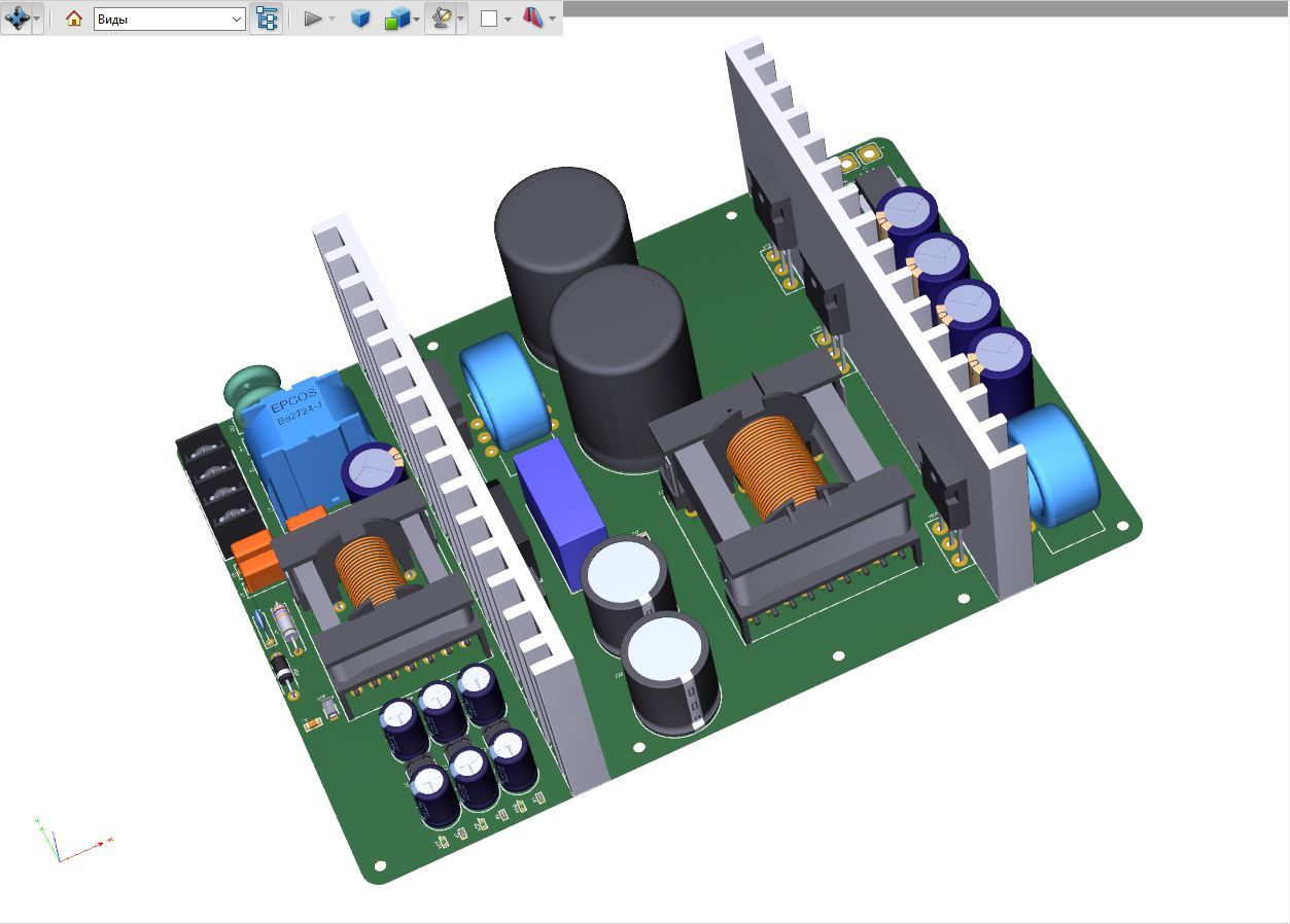
Figure 13 - 3D view of the board after the placement of components
3) Now, having determined the location and the general structure, we arrange the remaining components and “we part” the board. The design of the board can be done in two ways: manually and with the help of the autotracer, having previously described its actions with a couple of dozen rules. Both methods are good, but I’ll make this board all the same, because There are few components and there are no special requirements for leveling lines and signal integrity, and there should not be. So it will definitely be faster, autotracing is good when there are a lot of components (from 500 onwards) and the main part of the circuit is digital. Although if someone is interested, I can show you how to “dilute” the boards automatically in 2 minutes. The truth before this will have to write the rules all day, heh.
After 3-4 hours of “witchcraft” (half the time the models were missing the missing ones) with temperature and a cup of tea, I finally spread the board. I did not even think about saving space, many will say that the dimensions could be shrunk by 20-30% and will be right. I have a piece copy and to spend my time, which is clearly more expensive than 1 dm 2 for a double-layer board, it was just a pity. By the way, about the price of the board - when ordering at Resonit, 1 dm 2 of a double-layer board of a standard class costs about 180-200 rubles, so there is not much to save here if you don’t have a batch of 500+ pieces. Based on this, I can advise - do not pervert with a decrease in area, if 4 class and no requirements for dimensions. And that's what happened at the exit:
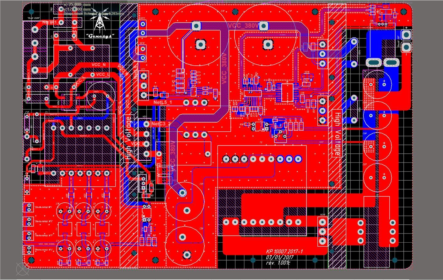
Figure 14 - Board design for a switching power supply
In the future, I will design the case for this device and I need to know its overall dimensions, as well as be able to “try on” it inside the case so that it does not become clear at the final stage, for example, that the main board interferes with the connectors on the case or the display. To do this, I always try to render all components in 3D, the output is this result and the file in the .step format for my Autodesk Inventor :
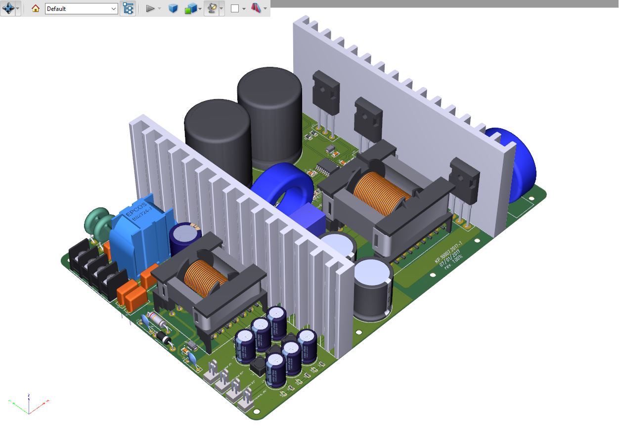
Figure 15 - Three-dimensional view of the resulting device
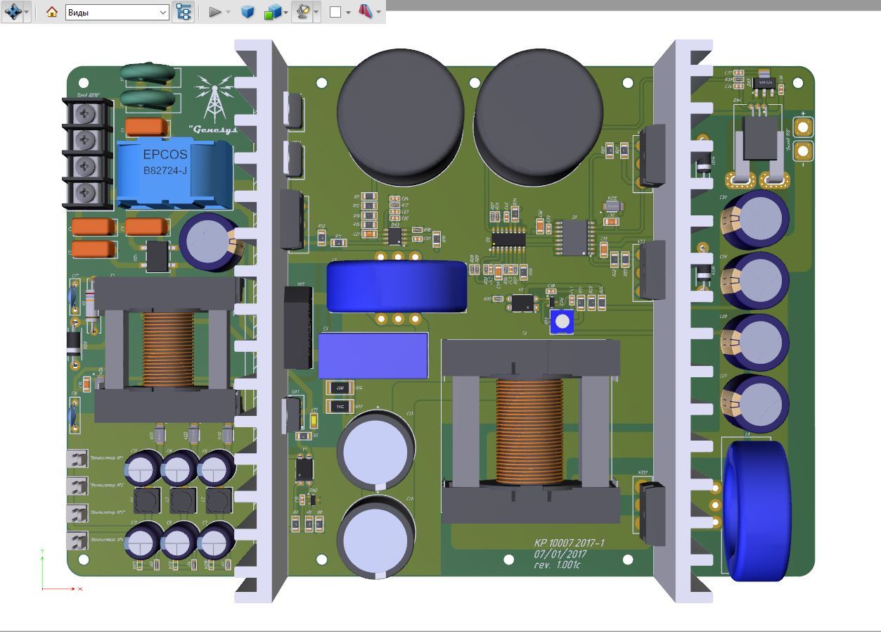
Figure 16 - Three-dimensional view of the device (top view)
Now the documentation is ready. Now it is necessary to generate the necessary batch of files for ordering the components, I have all the settings already registered in Altium, so everything is unloaded with one button. We need Gerber-files and the NC Drill file, in the first one there is information about the layers, in the second coordinate of the drill. You can see the file for uploading documents at the end of the article in the project, it looks like this:
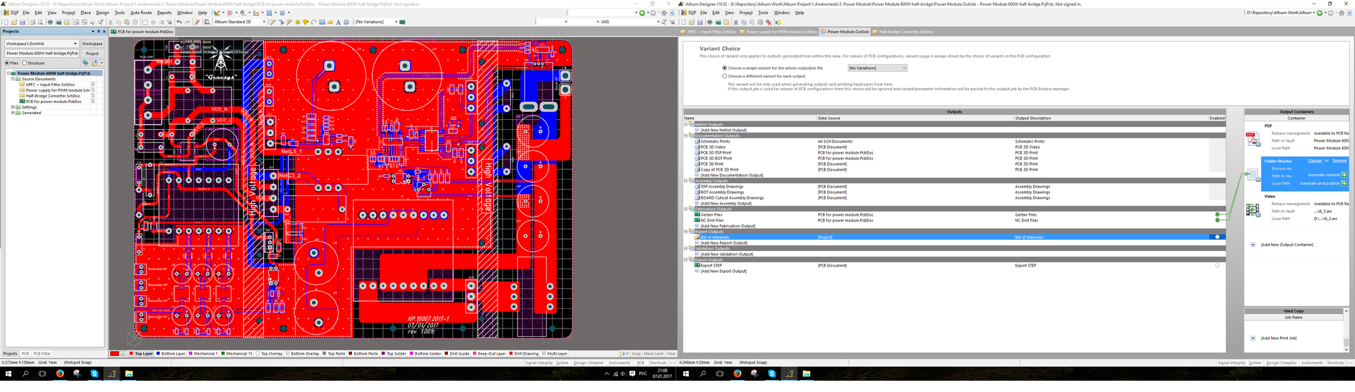
Figure 17 - Formation of a package of documentation for ordering printed circuit boards
Once the files are ready, you can order the board. Specific manufacturers will not recommend, for sure there is better and cheaper for prototypes. I order all the boards of the standard class 2,4,6 layers in Rezonite, in the same place there are 2 and 4 layer boards of the 5th class. Class 5 boards, where 6-24 layers in China (for example, pcbway), but HDI and 5th class boards with 24 or more layers are already only in Taiwan, all the same, the quality to China is still lame, and where the price tag is not limping not so nice. This is all about prototypes!
Following my convictions, I go to Resonit, oh, how many nerves they battered and drank the blood ... but lately they seem to have corrected and started to work more adequately, albeit with kicks. I create orders through my personal account, enter data about the board, upload files and send. I like their personal account; by the way, it considers the price by the way, and it is possible by changing the parameters to achieve a better price without loss of quality.
For example, now I wanted a 2 mm PCB board with 35 µm copper, but it turned out that such an option is 2.5 times more expensive than the one with 1.5 mm textolite and 35 µm - so I chose the latter. To increase the rigidity of the board, I added additional holes for the racks - the problem is solved, the price is optimized. By the way, if the fee went into a series, then somewhere on 100 pieces, this difference would have gone 2.5 times and the prices would be equal, because then a non-standard sheet was purchased for us and spent without balance.

Figure 18 - The final form of calculating the cost of boards
The final cost is determined: 3618 rubles . Of these, 2100 is preparation, it is paid only once for the project, all subsequent repetitions of the order go without it and pay only for the area. In this case, 759 rubles for a fee of 3.3 dm 2 , the larger the series, the lower the cost, although it is now 230 rubles / dm 2 , which is quite acceptable. Of course, it was possible to make an urgent production, but I often order, I work with one manager and the girl always tries to push through the order faster if the production is not loaded - in the end, and with the option “small series” for a period of 5-6 days, it’s enough to communicate politely and Do not be rude to people. Yes, and I have nowhere to hurry, so it was decided to save about 40%, which is at least pleasant.
Epilogue
Well, I came to the logical conclusion of the article - getting circuitry, board design and ordering boards for production. In total there will be 2 parts, the first is in front of you, and in the second I will tell you how I installed, assembled and debugged the device.
As promised, I share the source code of the project and other products of activity:
1) The source code of the project in Altium Designer 16 - here ;
2) Files for ordering printed circuit boards - here . Suddenly you want to repeat and order, for example, in China, this archive is more than enough;
3) Diagram of the device in pdf - here . For those who do not want to spend time installing Altium from a telephone or for review (high quality);
4) Again, for those who do not want to install heavy software, but it is interesting to twist a piece of metal I post the 3D model in pdf - here . To view it is necessary to download the file, when you open in the upper right corner click "trust the document only once", then poke into the center of the file and the white screen turns into a model.
Just want to ask the opinion of the readers ... Now the boards are ordered, the components too - in fact there are 2 weeks about what to write an article? In addition to such "mutants" like this, sometimes you want to make something miniature, but useful, I presented several options in the polls, or offer your version probably in a personal, so as not to clutter up comments.
Source: https://habr.com/ru/post/400381/
All Articles