Small secrets trace boards with operating and instrumentation amplifiers
When designing boards
Nothing is so cheap
And not valued so highly
Like the correct tracing.

In the age of the Internet of things and the availability of manufacturing printed circuit boards,
Even when tracing a simple digital board, there are unwritten rules that I always follow in my projects, and in the case of developing measuring devices with digital-analogue circuit sections, this is simply necessary.
')
In this article, I want to turn novice designers to a number of elementary techniques that should be followed to obtain a stable working circuit and reduce measurement error or minimize the distortion factor of the audio path. For clarity, the information is presented in the form of consideration of two examples.
The recommendations are very simple and known to many, however, as my practice has shown, it is far from always even experts with experience adhere to them.
Example number two. Trace simple op amp circuit
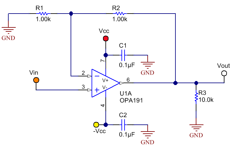
Fig. 1. Amplifier circuit at the shelter
To begin, consider the simplest example. Just a few resistors and capacitors are a non-inverting amplifier with a voltage gain of 2. Set ourselves the task of optimizing the area tracing and consider two options. The board in both cases is double-layered, the upper signal layer is red, the bottom is blue. The right option is not only slightly smaller in area, the main thing in it is less likely to cause parasitic connections.

Fig. 2. Two options for tracing the amplifier board at the OS
First, pay attention to how the blocking capacitor C2 is installed on the right side of the figure - at the minimum distance from the power supply terminal. Secondly, the negative voltage coming from the source first goes to the capacitor and only from there to the OU power supply. This simple technique greatly increases the efficiency of the blocking capacitor. I did the same with capacitor C1. By the way, if you use several blocking capacitors, for example, tantalum of large capacity and ceramic less, then the capacitor of smaller capacity should be located closer to the power supply, since it has less parasitic inductance and suppresses high-frequency noise better.
A small offtopic, not directly related to the topic of today's article
I strongly advise you to use the same technique when applying power to other types of microcircuits, especially ADC, DAC, and numerous power supply pins of microcontrollers. If you use the built-in analog modules of the microcontroller - ADC, DAC, comparators, reference sources, do not be too lazy to look into the datasheet and see which blocking capacitors are in what quantity and where to install. The interchange circuit in the form of a filter or at least resistance between the main digital power supply of the microcontroller and the analog one will not interfere. It is better to place analog ground with a separate polygon or screen layer , and connect with the main ground at one point, in some cases it is useful through the filter
The elements of the feedback circuit should be located as close as possible to the non-inverting input, which minimizes the possibility of interference to the high-resistance input circuit.
Instead of separate ground conductors, grounding of the lower layer of the board with a
We proceed to a more serious and interesting case from the field of measurements, where the trace is important for archives.
Example number one. Trace consumption current monitor on instrument amplifier

Fig. 3. Scheme of the current monitor using instrumental OS
The figure shows a diagram of the meter consumed current. The measuring element is the resistance of the shunt included in the supply circuit. The load on which the current is measured - R load. The measured voltage is removed from the resistance R shunt and filtered using a symmetrical circuit on the elements R1, R2, C1-C3. Chip U2 is used to supply the reference voltage. R4, C5 - output filter.
When tracing, of course, you must follow all the recommendations that were given above.

Fig. 4. Two options for tracing the amplifier board on the instrumental OS
Let us analyze the shortcomings that the left scheme has:
- Since we have a differential input, it is necessary to make its two signal circuits as symmetrical as possible. The conductors of the signal lines should be of the same length and close to each other. Ideally at the same distance from each other;
- The resistor driving the gain of the instrumentation amplifier should be located as close as possible to the pins of the microcircuit. Even a small parasitic capacitance between conductors that go to it in the left figure can lead to a loss of stability of the instrumentation amplifier. In general, feedback loops should be as short as possible;
- The repeater chip of the reference source must be located as close as possible to the input of the reference voltage of the instrumentation amplifier.
By following very simple rules you make your life easier. In some cases, they simply do not cause harm, in others they can significantly improve both the stability of the circuit as a whole and the measurement accuracy.
Do not hold a loaded rifle on the wall. One day it will surely shoot and choose the most inconvenient moment for this.
In preparing this article, TI experts blog materials were used.
Source: https://habr.com/ru/post/399955/
All Articles