Germanium can replace silicon in transistors and bring them to a new level
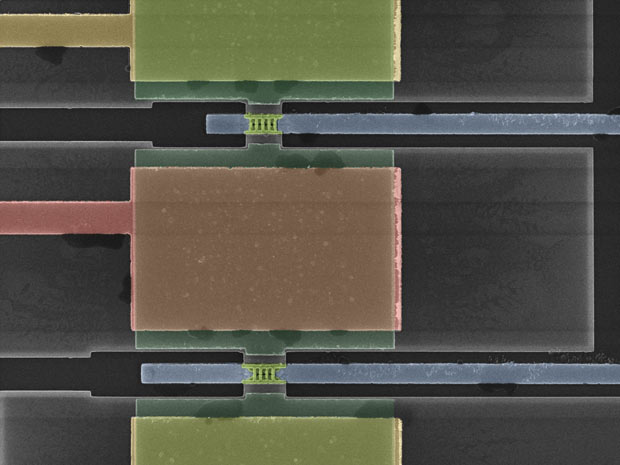
As a demonstration of the concept's performance, the team created a germanium substrate on an insulator with a team to create inverters containing planar transistors first and then FinFET transistors
Almost 70 years ago, two physicists from Bell's Telephone Lab, John Bardeen and Walter Brattain [John Bardeen and Walter Brattain], pressed two thin gold contacts into a germanium plate, and made the third contact from the bottom of the plate. The current passing through this structure could be used to turn a weak signal into a strong one. As a result, the first transistor appeared - an amplifier and a switch, which may have become the greatest invention of the 20th century. Thanks to Moore's law, the transistor developed computers far beyond what seemed possible in the 1950s.
Despite the stellar role of Germany in the early history of transistors, it was soon replaced by silicon. But now, surprisingly, this material is ready to return. Leaders in the production of chips are thinking about replacing components in the heart of the transistor - the conductive channel. The idea is to replace silicon with a material that is better able to conduct current. Creating transistors with such channels can help engineers continue to improve circuit performance in speed and energy efficiency, which will mean the emergence of improved computers, smartphones, and many other gadgets in subsequent years.
For a long time, interest in alternative channels revolved around compounds A III B V , such as gallium arsenide, consisting of atoms to the left and right of silicon in the periodic table. And I participated in that study. Eight years ago I wrote an article for this magazine , denoting the progress made in building transistors on such connections.
')
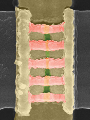
The two transistors in the FinFET-based inverter contain fin channels that stand out from the plane of the substrate (pink channels at the top, pink channels at the bottom, and another set of beveled views). The distances between the "fins" at the top are tens of nanometers.
But as a result, we found that the approach with A III B V there are fundamental physical limitations. And also, it would most likely be too expensive and difficult to integrate with existing silicon technology. So a few years ago, my team at Purdue University began experimenting with another device: with a transistor, the channel of which is made of germanium. Since then, we have demonstrated the first CMOS circuits (the complementary metal-oxide-semiconductor structure) [CMOS, complementary metal-oxide-semiconductor]. Approximately the same logic that is inside modern computers, only made from germanium grown on ordinary silicon substrates. We also created a number of different transistor architectures from this material. They include nanowire devices, which can be the next production step, when today's best transistors, FinFET, can no longer be further reduced.
And what is even more interesting, it turns out that returning germanium to work is not as difficult as it seems. Transistors using a combination of silicon and germanium in the channel can already be found in new chips, and they first appeared in 2015, in a demonstration of future chip manufacturing technologies from IBM. These developments can be the first step of the industry, seeking to introduce more and more shares of Germany into the channels. After a few years, we may be faced with the fact that the material that gave us the transistors helped to transfer them to the next era of outstanding performance.
Germanium was first isolated and discovered by the German chemist Clemens Winkler at the end of the XIX century. The material was named after the scientist's homeland, and was always considered to be a poorly conducting current. This changed during the Second World War, when the semiconductor properties of germanium were discovered - that is, the ability to switch between conducting and blocking current. In the postwar years, semiconductor devices developed rapidly in Germany. In the United States, production, responding to market demands, increased from a few hundred pounds in 1946 to 45 tons by the 1960s. But silicon won; It has become a popular material for logic and memory chips.
There are good reasons for the dominance of silicon. First of all, there are more, and it is cheaper. Silicon has a wider forbidden zone, an energy barrier that must be overcome to create conductivity. The larger this zone, the more difficult the current to leak through the device at an unnecessary time and waste energy. As a bonus, silicon and thermal conductivity were better, which made it easier to remove heat so that the circuits do not overheat.
Considering all the advantages, it is natural to be interested - why would we even think about the return of Germany to the channel. The answer is mobility. Electrons in germanium at room temperature move almost three times more readily than in silicon. And the holes - the absence of an electron in the material, considered as a positive charge - move almost four times more readily.
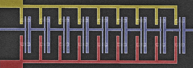
Nine-stage CMOS oscillator, introduced in 2015
The fact that in Germany electrons and holes are so mobile makes it a convenient candidate for CMOS circuits. CMOS combines two different types of transistors: p-channel FET (pFET), the channel of which contains an excess of free holes, and n-channel FET (nFET), which have an excess of electrons. The faster they move, the faster the contours work. A decrease in the voltage required for their movement also means a decrease in energy consumption.
Of course, germanium is not the only material with such particle mobility. The previously mentioned A III B V compounds, materials such as indium arsenide and gallium arsenide, can also boast of high electron mobility. Electrons in indium arsenide are almost 30 times more mobile than in silicon. But the problem is that this property does not apply to holes - they are not much more mobile than those in silicon. And this restriction makes it impossible to create high-speed pFETs, and the lack of high-speed pFETs nullifies obtaining fast CMOS circuits, since they cannot work with a very large difference in the speeds of nFETs and pFETs.
One solution is to take the best from each material. Researchers in many laboratories, for example, the European semiconductor research organization Imec and the Zurich laboratory of IBM, have shown ways to create circuits in which nFET channels are made of compositions A III B V and pFET from germanium. And although this technology may allow you to create very fast contours, it greatly complicates production.
Therefore, we prefer the simple approach with germanium. German channels should increase speed, and production problems will not be so serious.
How is germany
| Property | Silicon (Si) | Germanium (Ge) | Gallium Arsenide (GaAs) | Indium Arsenide (InAs) | Units |
| Forbidden Zone | 1.12 | 0.66 | 1.42 | 0.35 | eV |
| Electron mobility at 300 K | 1,350 | 3,900 | 8,500 | 40,000 | cm 2 / (V · s) |
| Hole mobility at 300 K | 450 | 1,900 | 400 | 500 | cm 2 / (V · s) |
| Maximum possible electron velocity | one | 0.6 | 2 | 3.5 | x10 7 cm / s |
| Critical electric field | 0.25 | 0.1 | 0.004 | 0.002 | x10 6 V / cm |
| Thermal conductivity | 1.5 | 0.58 | 0.5 | 0.27 | W / (cm · K) |
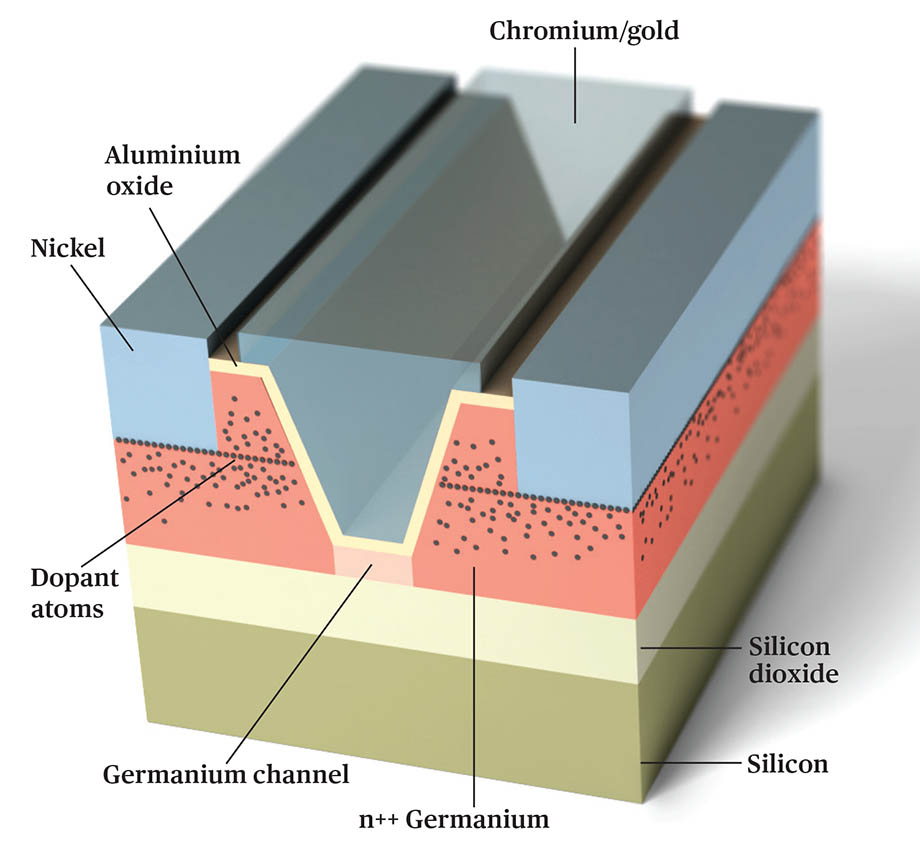
In order for germanium - or any alternative material - to go into production, it is necessary to find a way to add it to the silicon substrates currently used to make chips. Fortunately, there are many ways to apply a germanium layer on the silicon substrate, from which you can then make channels. The use of a thin layer eliminates two key problems of germanium - the high cost compared to silicon, and the relatively poor thermal conductivity.
But to replace the silicon in the transistor, it is not enough just to cram a thin and high-quality layer of germanium. The channel should work flawlessly with the other components of the transistor.
In the ubiquitous modern CMOS chips, MOS-based transistors are used (metal oxide semiconductor - MOSFET; metal-oxide-semiconductor field effect transistor - MOSFET). He has four basic parts. The source and drain are the starting and ending point of the current movement; the channel connecting them; a shutter serving as a valve controlling the presence of current in the channel.
In reality, other ingredients are present in a quality transistor. One of the most important is the gate isolator, which prevents the gate and channel from short-circuiting. Atoms in semiconductors, such as silicon, germanium and A III B V compounds, are arranged in three dimensions. An ideally flat surface cannot be made, therefore the atoms located at the top of the channel will have several protruding bonds. You need an insulator that binds as many of these connections as possible, and this process is called passivation, or surface etching. In the case of poor-quality manufacturing, you can get a channel with "electric potholes", full of such places where charge carriers can temporarily linger, which reduces their mobility and, as a result, the speed of the device.

Left: nFET of A III B V , and germanium pFET formulations; pieces of both materials are grown on an insulated silicon substrate.
Right: both transistors are made of germanium bonded to the substrate.
Fortunately, nature has supplied silicon with a natural insulator, well matching its crystal structure: silicon dioxide (SiO 2 ). And although in modern transistors there are more exotic insulators, they still have a thin layer of this oxide, which serves to passivate the silicon channel. Since silicon and SiO 2 are close in structure, a well-made SiO 2 layer binds 99,999 out of 100,000 free bonds — and there are about as many of them per square centimeter of silicon.
Gallium arsenide and other compounds of A III B V do not have natural oxides, and germanium does have it - therefore, in theory, it should have ideal material for passivating the channel. The problem is that germanium dioxide (GeO 2 ) is weaker than SiO 2 , and can be absorbed and dissolved by the water used to clean the substrates during chip manufacturing. Worse, the growth process of GeO 2 is difficult to control. An ideal device requires a layer of GeO 2 1-2 nm thick, but in reality it is more difficult to make a layer thinner than 20 nm.
Researchers studied various alternatives. A Stanford professor, Krishna Saraswat, and his colleagues, who spurred interest in using germanium as an alternative material back in the 2000s, first studied zirconium dioxide, a material with a high dielectric constant of the type used in high-speed transistors today. Based on their work, a group from Imec in Belgium studied what can be done with a superfine silicon layer to improve the interface between germanium and similar materials.
But passivation of Germany was seriously improved in 2011, when the team of Professor Shinichi Takagi [Shinichi Takagi] from the University of Tokyo showed a way to control the growth of a germanium insulator. First, researchers have grown a nanometer layer of another insulator, aluminum oxide, on the germanium channel. After that, they were placed in an oxygen chamber. Part of the oxygen passed through the aluminum oxide layer to the lower germanium, and mixed with it, forming a thin oxide layer (the compound of germanium with oxygen, but technically not GeO 2 ). Aluminum oxide not only helps to control growth, but also serves as a protective coating for a less stable layer.
Nanowire channels
A few years ago, inspired by this discovery and given the difficulty of creating pFETs with channels from A III B V , my group in Perdue began exploring ways to create transistors on germanium channels. We started with the use of substrates with germanium on an insulator, developed by the French manufacturer Soitec. These are standard silicon substrates with an insulating layer under a 100 nm germanium layer.
With these substrates, you can create transistors, in which all standard parts - source, channel and drain - are made of germanium. The transistor manufacturer does not have to follow this design, but it was easier for us to study the basic properties of germanium devices.
One of the first obstacles was the fight against resistance between the source and drain of the transistor and the metal electrodes connecting them to the outside world. Resistance arises from the natural Schottky electron barrier appearing at the point of contact of the metal and semiconductor. Silicon transistors have been tirelessly optimized to minimize this barrier so that charge carriers can easily overcome it. But in the germanium device tricky engineering solutions are required. Due to the nuances of the electronic structure, holes easily move from metal to germanium, but electrons are not very. This means that nFETs that rely on the movement of electrons will have very high resistance, loss of heat and current.
The standard way to make the barrier thinner is to add more dopant to the source and drain. The physics of the process is complex, but it can be represented as follows: more impurity atoms introduce more free charges. With an abundance of free charge carriers, the electrical interaction between the metal electrodes and the semiconductor source and drain increases. This helps to enhance the tunnel effect.
Unfortunately, this technology works worse with germanium than with silicon. The material does not withstand high concentrations of dopants. But we can use those places where the density of impurities is maximum.
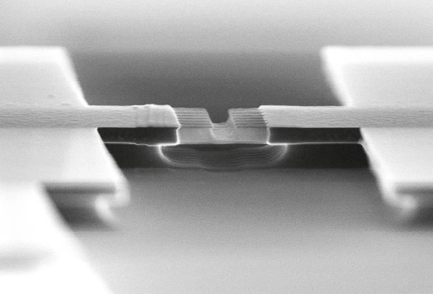
To do this, we use the fact that impurities are added to modern semiconductors by ultrahigh electric fields pushing ions into the material. Some of these atoms stop immediately, while others penetrate deeper. As a result, you will get a normal distribution: the concentration of impurity atoms at a certain depth will be maximum, and then when moving inwards or in the opposite direction will decrease. If we deepen the electrodes of the source and drain into a semiconductor, we can place them in places of the highest concentration of impurity atoms. This dramatically reduces the problem of contact resistance.
Contacts are immersed to the depth of the maximum concentration of impurity atoms
Regardless of whether chip makers use this approach to reduce the Schottky barrier in Germany, this is a useful demonstration of its capabilities. At the beginning of our study, the best that germanium nFETs showed was a current of 100 μA for each μm width. In 2014, at the VLSI Technology and Circuits Symposium in Hawaii, we reported on germanium nFETs capable of transmitting 10 times more current, which is roughly comparable to silicon. After six months, we demonstrated the first circuits containing germanium nFET and pFET, a necessary prerequisite for the manufacture of modern logic circuits.
Since then, we have used germanium to build more advanced transistors, such as FinFET - the state of the art. We even made nanowire transistors in Germany, which in the coming years could replace FinFET.
These developments will be required in order to use germanium in mass production, because with their help you can better control the channel of the transistor. Due to the small forbidden zone of germanium, such a transistor requires only a quarter of the energy needed to switch to the conductive state of a silicon transistor. This opens up opportunities for low-energy work, but it also makes it more likely that a current will leak when it should not. A device with better control over the channel will allow manufacturers to use a small forbidden zone without compromise with speed.
We took a good start, but we still have a job. For example, additional experiments with substrates are needed, which should show transistors with high-quality germanium channels. You also need to make design improvements to speed up.
Of course, germanium is not the only option for transistors of the future. Researchers continue to study compounds A III B V , which can be used both with germanium and in isolation. The number of possible transistor improvements is huge. This list includes transistors on carbon nanotubes , vertically oriented switches, three-dimensional circuits, channels made from a mixture of germanium and tin, transistors based on the principle of quantum tunneling.
In the coming years, perhaps, we will adapt some of the listed technologies. But the addition of germanium — even in a mixture with silicon — is a solution that will allow manufacturers to continue to improve transistors in the near future. Germanium, the original material of the semiconductor era, could be the panacea for its next decade.
Source: https://habr.com/ru/post/399717/
All Articles