Subtleties of designing the power board of the inverter
Hello! With modest steps, I continue the cycle of articles about the development of iron electric bait. Let's start with the most interesting thing - the inverter that controls the motor. I want to tell you more about the intricacies of building a power board and about the temperature regime of transistors.
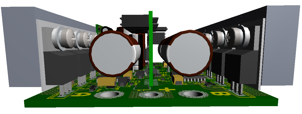
Warp core model electric bait
The main problem in designing a board for high high-frequency currents is the inductance of conductors, capacitors, transistors, or rather the resulting emissions due to it and the need to lay a supply of parameters for the keys, which leads to higher design costs and increased switching losses.
In the process of work on an inductive load, when the current is broken, voltage surges on the key occur, which are ∆V = -L (dI / dt), where ∆V is the magnitude of the voltage change, L is the inductance, dI / dt is the rate of current change (rise or decrease).
')
Take the special case of PWM of two phases, where the current initially flows through the closed switch Q2, and then the current builds up in the motor circuit through the upper switch Q1. The Q6 key for simplicity is always on.

The red direction indicates the path of the initial current flow. At the moment of switching, the key Q2 opens, but at the same time, the voltage on this key goes to minus by the amount of incidence on the parasitic MOSFET diode. This is due to the fact that the inductance of the motor, in which energy is stored, tries to "save" its current, and creates a negative voltage. Next, the Q1 key starts to turn on, the current gradually increases on the inductances L_DC +, L_Q1D, L_Q1S, L_DC. Where L_QnD is the inductance of the drain of the transistor case, and L_QnS is the inductance of the source, and L_DC is the inductance of the board. In the process of current transfer from one part of the circuit to another, the transistor Q2 can suddenly detect on itself a voltage greater than that supplied through the power supply bus and installed on the input capacitance.

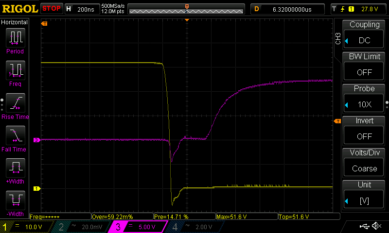
An example of switching at a current of 100A
The magnitude of this voltage will be proportionally greater than the switching speed. We do not want to allocate a lot of heat on the keys in the process of switching, so the ideal option is when the key switches instantly, but this is not achievable in reality. Simply put, the faster this transition occurs, the less active losses will be in the key, but at the same time, the faster the transition occurs, the greater will be the surges in voltages arising at L_DC, L_Q1D, L_Q1S. Another rarely mentioned, but perhaps the most parasitic phenomenon in this process is the charge of the diode Q2. Since there is a delay between the switching off of Q2 and turning on Q1, the dead time, the charge recovery charge accumulates on the diode Q2, in the documentation for the transistor is specified as Qrr, measured in nanocolons. In the process of switching on Q1, a through current arises which restores the parasitic diode Q2. The magnitude of this current will be higher, the faster it is required to turn on Q1 and the more current passes through the transistor. This additionally causes a surge voltage on L_Q2D, L_Q2S. Such a switch is called “hard” from English. hard commutation.
If the transistor was chosen without voltage margin, such a surge could lead to avalanche current (avalanche), which would greatly reduce the life of the transistor, and with long-term exposure it could completely disable it.

In the process of such switching, RF oscillations (“ringing”, of the order of a pair of MHz) can occur, inductance L_Q (1,2) S and parasitic capacitances between the gates of Q1 / 2 transistors and their drain are involved in their occurrence. As in the conventional TO220 3pin case, the control signal is actually fed through the power leg, which introduces its own interference. To solve this problem, a separate pin source for the control signal, which has no power pickup, is displayed in the power assemblies-modules. At the moment of opening of the transistor Q1, the current starting to flow through the source creates a voltage drop on the inductance of the source-legs of the transistor, which slows down the opening. In addition, this process is hampered by a sharp voltage drop, which also dampens the gate control signal through the parasitic capacitance. On the other hand, on the transistor Q2, a sharp rise in the voltage Vds occurs, which pulls the gate to open through the parasitic capacitance between the drain and the gate. The combination of all these factors leads to the appearance of HF oscillations, the fight against them is usually done by reducing the steepness dI / dt and dVds / dt, but there is an optimum between the opening speed, the opening loss, and the ringing loss of the transistor.
An example of a "soft" off Q1 with a view from Q2.
Negative voltage on Vds (1) - inductance of legs Q2. At the gate (3) only half of this outlier is visible, since in this case, in the oscilloscope connection circuit, the current changes only on the source leg.
Consider the option of two conductors of the same width, but with a different location on the board.

Suppose we have a track width of 10mm, length 100mm, and the distance between them is 0.5mm. For option a, mutual inductance will be ~ 6.3 nH. For option b, the inductance will be ~ 132nH. What does it mean? Take the current change rate of 1.25A / nS, as in the screenshot above, following the formula ∆V = -L (dI / dt), we obtain the voltage change for option a ∆V = -6.3 nH * 1.25A / ns = 7.8V. For option b, this value will be 132nH * 1.25A / ns = 165V. This is much higher than our supply voltage! In fact, a breakdown will occur, and the voltage will rest on the voltage limit of the transistor, and the current will flow through it, despite the fact that it is closed. Therefore, there will be no sense from your good capacitors if they hang on long “inductances” :)
What could possibly go this way ?
As for the parasitic components of the transistor case, they will not particularly deal with them, the shortest legs to the board, no long wires. High-frequency ringing well shunts ceramic capacitors, they should be placed directly next to the keys along the power bus, but you can completely get rid of the ringing by eliminating the parasitic diode of the transistor, using SiC transistors or adaptive control, but this is a different price range. Another option for reducing the inductance of the case are SMD transistors, the so-called. DirectFet, PowerQFN and the like. But they also have their drawbacks, they can be attributed to a worse heat sink, the complexity of the layout with SMD installation and, of course, the price.
Anyway, the inverter in work will generate heat. More current - more heat. Since in the motor, the current may briefly exceed the average value at the moments of acceleration and deceleration, for transistors it is required to ensure normal thermal conditions for such load peaks. Standardly for a silicon crystal, the maximum temperature Tj = 175 ° C is indicated.

At the moments of switching transistors there are sharp large emissions of heat - active losses. Passive losses are losses on the drain-source channel resistance in the open state, are more constant in time and easier to calculate. For short-term thermal bursts, the copper substrate of the transistor itself acts as a good heat buffer, another minus of the SMD components — they are noticeably smaller. The thermal resistance from the crystal to the case at the transistor chosen by me is 0.57 ° C / W, which means that by releasing it 50 watts of heat constantly, a temperature gradient of 29 ° C is formed. For thermal emissions, it is also required to leave a certain margin and take into account a certain delay on the thermocouple, therefore, the final optimum value of the transistor case was chosen to be 100 ° C. The question arises - how long can the maximum current be given before overheating? Various thermal interfaces have been tested, even boards with an aluminum base. On the quality of heat transfer from the base of the transistor to the radiator, I would arrange the materials in this order, in descending order of thermal conductivity:
Direct contact through thermal grease
Aluminum nitride substrates + thermal grease (2sl)
Board with aluminum base
Aluminum oxide substrates + thermal grease (2sl)
Silicone flexible supports + thermal grease
Silicone flexible substrates without thermal paste
Direct contact is not our option, as it does not provide electrical insulation of the transistor housing from the radiator. With a small margin from the aluminum board was a substrate of aluminum oxide. Nitride was noticeably more expensive and less affordable. According to the tests between the silicone substrate and the ceramic of aluminum oxide, the difference was almost 2 times; in the duration of the full load, 1 minute and 30 seconds, respectively. Of course, this test does not pretend to high scientific accuracy, but with a penny price difference, it is twice as long to “tumble” on a bike? The final choice, of course, was ceramics based on aluminum oxide! As it turned out, mounting is even easier with it, and another bonus is that the transistor is bent much less when the screw is tightened. The clamp, judging by the trace of the thermal paste, has always been uniform. What can not be said about the flexible substrate.

With standard mounting to the radiator through the eye using a screw, the silicone gasket tends to shrink, which can lead to uneven surface contact. Therefore, the last item is “substrate without thermal paste”, since she, thermal paste, in this case somewhat compensated for this effect. Of course, in such cases, it is recommended to use a special spring that will evenly press the entire body of the transistor, but we did not have the opportunity to accommodate those to fit into the envelope.
Riding a Chinese controller, I often noticed that he had only one side hot, and the other remained cold. Therefore, the final layout of the power switches was made so as to warm up the entire body as equally as possible. The keys were installed on both sides, through a small aluminum adapter.
In this article, I described the most interesting things in my opinion. Of course, the choice of the MOS transistor itself according to its characteristics, the calculation of heat losses on the chip and the heating of electrolytic capacitors under the influence of a pulsating current remained behind the scenes. In the next article we will touch on the device circuitry, current digitization options and the implementation of current protection.
Warp core model electric bait
The main problem in designing a board for high high-frequency currents is the inductance of conductors, capacitors, transistors, or rather the resulting emissions due to it and the need to lay a supply of parameters for the keys, which leads to higher design costs and increased switching losses.
In the process of work on an inductive load, when the current is broken, voltage surges on the key occur, which are ∆V = -L (dI / dt), where ∆V is the magnitude of the voltage change, L is the inductance, dI / dt is the rate of current change (rise or decrease).
')
Take the special case of PWM of two phases, where the current initially flows through the closed switch Q2, and then the current builds up in the motor circuit through the upper switch Q1. The Q6 key for simplicity is always on.
The red direction indicates the path of the initial current flow. At the moment of switching, the key Q2 opens, but at the same time, the voltage on this key goes to minus by the amount of incidence on the parasitic MOSFET diode. This is due to the fact that the inductance of the motor, in which energy is stored, tries to "save" its current, and creates a negative voltage. Next, the Q1 key starts to turn on, the current gradually increases on the inductances L_DC +, L_Q1D, L_Q1S, L_DC. Where L_QnD is the inductance of the drain of the transistor case, and L_QnS is the inductance of the source, and L_DC is the inductance of the board. In the process of current transfer from one part of the circuit to another, the transistor Q2 can suddenly detect on itself a voltage greater than that supplied through the power supply bus and installed on the input capacitance.
An example of switching at a current of 100A
The magnitude of this voltage will be proportionally greater than the switching speed. We do not want to allocate a lot of heat on the keys in the process of switching, so the ideal option is when the key switches instantly, but this is not achievable in reality. Simply put, the faster this transition occurs, the less active losses will be in the key, but at the same time, the faster the transition occurs, the greater will be the surges in voltages arising at L_DC, L_Q1D, L_Q1S. Another rarely mentioned, but perhaps the most parasitic phenomenon in this process is the charge of the diode Q2. Since there is a delay between the switching off of Q2 and turning on Q1, the dead time, the charge recovery charge accumulates on the diode Q2, in the documentation for the transistor is specified as Qrr, measured in nanocolons. In the process of switching on Q1, a through current arises which restores the parasitic diode Q2. The magnitude of this current will be higher, the faster it is required to turn on Q1 and the more current passes through the transistor. This additionally causes a surge voltage on L_Q2D, L_Q2S. Such a switch is called “hard” from English. hard commutation.
If the transistor was chosen without voltage margin, such a surge could lead to avalanche current (avalanche), which would greatly reduce the life of the transistor, and with long-term exposure it could completely disable it.
In the process of such switching, RF oscillations (“ringing”, of the order of a pair of MHz) can occur, inductance L_Q (1,2) S and parasitic capacitances between the gates of Q1 / 2 transistors and their drain are involved in their occurrence. As in the conventional TO220 3pin case, the control signal is actually fed through the power leg, which introduces its own interference. To solve this problem, a separate pin source for the control signal, which has no power pickup, is displayed in the power assemblies-modules. At the moment of opening of the transistor Q1, the current starting to flow through the source creates a voltage drop on the inductance of the source-legs of the transistor, which slows down the opening. In addition, this process is hampered by a sharp voltage drop, which also dampens the gate control signal through the parasitic capacitance. On the other hand, on the transistor Q2, a sharp rise in the voltage Vds occurs, which pulls the gate to open through the parasitic capacitance between the drain and the gate. The combination of all these factors leads to the appearance of HF oscillations, the fight against them is usually done by reducing the steepness dI / dt and dVds / dt, but there is an optimum between the opening speed, the opening loss, and the ringing loss of the transistor.
An example of a "soft" off Q1 with a view from Q2.
Negative voltage on Vds (1) - inductance of legs Q2. At the gate (3) only half of this outlier is visible, since in this case, in the oscilloscope connection circuit, the current changes only on the source leg.
Techniques to combat parasitic inductance
Consider the option of two conductors of the same width, but with a different location on the board.
Suppose we have a track width of 10mm, length 100mm, and the distance between them is 0.5mm. For option a, mutual inductance will be ~ 6.3 nH. For option b, the inductance will be ~ 132nH. What does it mean? Take the current change rate of 1.25A / nS, as in the screenshot above, following the formula ∆V = -L (dI / dt), we obtain the voltage change for option a ∆V = -6.3 nH * 1.25A / ns = 7.8V. For option b, this value will be 132nH * 1.25A / ns = 165V. This is much higher than our supply voltage! In fact, a breakdown will occur, and the voltage will rest on the voltage limit of the transistor, and the current will flow through it, despite the fact that it is closed. Therefore, there will be no sense from your good capacitors if they hang on long “inductances” :)
What could possibly go this way ?
As for the parasitic components of the transistor case, they will not particularly deal with them, the shortest legs to the board, no long wires. High-frequency ringing well shunts ceramic capacitors, they should be placed directly next to the keys along the power bus, but you can completely get rid of the ringing by eliminating the parasitic diode of the transistor, using SiC transistors or adaptive control, but this is a different price range. Another option for reducing the inductance of the case are SMD transistors, the so-called. DirectFet, PowerQFN and the like. But they also have their drawbacks, they can be attributed to a worse heat sink, the complexity of the layout with SMD installation and, of course, the price.
About heat sink
Anyway, the inverter in work will generate heat. More current - more heat. Since in the motor, the current may briefly exceed the average value at the moments of acceleration and deceleration, for transistors it is required to ensure normal thermal conditions for such load peaks. Standardly for a silicon crystal, the maximum temperature Tj = 175 ° C is indicated.
At the moments of switching transistors there are sharp large emissions of heat - active losses. Passive losses are losses on the drain-source channel resistance in the open state, are more constant in time and easier to calculate. For short-term thermal bursts, the copper substrate of the transistor itself acts as a good heat buffer, another minus of the SMD components — they are noticeably smaller. The thermal resistance from the crystal to the case at the transistor chosen by me is 0.57 ° C / W, which means that by releasing it 50 watts of heat constantly, a temperature gradient of 29 ° C is formed. For thermal emissions, it is also required to leave a certain margin and take into account a certain delay on the thermocouple, therefore, the final optimum value of the transistor case was chosen to be 100 ° C. The question arises - how long can the maximum current be given before overheating? Various thermal interfaces have been tested, even boards with an aluminum base. On the quality of heat transfer from the base of the transistor to the radiator, I would arrange the materials in this order, in descending order of thermal conductivity:
Direct contact through thermal grease
Aluminum nitride substrates + thermal grease (2sl)
Board with aluminum base
Aluminum oxide substrates + thermal grease (2sl)
Silicone flexible supports + thermal grease
Silicone flexible substrates without thermal paste
Direct contact is not our option, as it does not provide electrical insulation of the transistor housing from the radiator. With a small margin from the aluminum board was a substrate of aluminum oxide. Nitride was noticeably more expensive and less affordable. According to the tests between the silicone substrate and the ceramic of aluminum oxide, the difference was almost 2 times; in the duration of the full load, 1 minute and 30 seconds, respectively. Of course, this test does not pretend to high scientific accuracy, but with a penny price difference, it is twice as long to “tumble” on a bike? The final choice, of course, was ceramics based on aluminum oxide! As it turned out, mounting is even easier with it, and another bonus is that the transistor is bent much less when the screw is tightened. The clamp, judging by the trace of the thermal paste, has always been uniform. What can not be said about the flexible substrate.
With standard mounting to the radiator through the eye using a screw, the silicone gasket tends to shrink, which can lead to uneven surface contact. Therefore, the last item is “substrate without thermal paste”, since she, thermal paste, in this case somewhat compensated for this effect. Of course, in such cases, it is recommended to use a special spring that will evenly press the entire body of the transistor, but we did not have the opportunity to accommodate those to fit into the envelope.
Riding a Chinese controller, I often noticed that he had only one side hot, and the other remained cold. Therefore, the final layout of the power switches was made so as to warm up the entire body as equally as possible. The keys were installed on both sides, through a small aluminum adapter.
Epilogue
In this article, I described the most interesting things in my opinion. Of course, the choice of the MOS transistor itself according to its characteristics, the calculation of heat losses on the chip and the heating of electrolytic capacitors under the influence of a pulsating current remained behind the scenes. In the next article we will touch on the device circuitry, current digitization options and the implementation of current protection.
Source: https://habr.com/ru/post/399693/
All Articles