Leading chip makers are eyeing photolithography in the deep ultraviolet
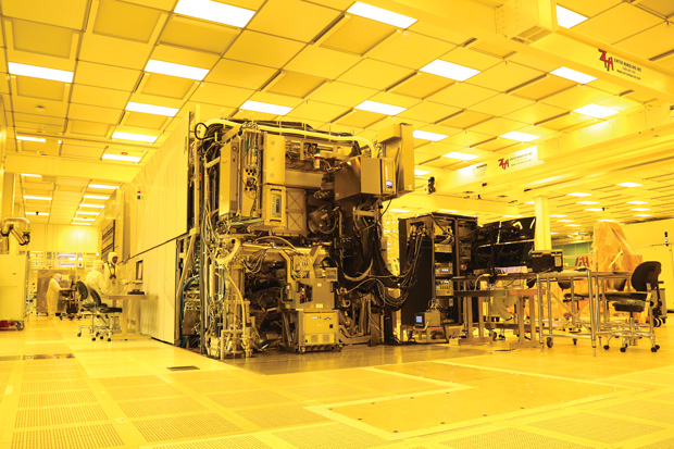
EUML scanner ASML NXE: 3300B prints chips in the laboratory of the Polytechnic Institute SUNY
Even after you put on a protective suit and entered the Fab 8 workshop, its scale is difficult to assess. Many rows of high-end “tools” occupy most of the space in the GlobalFoundries factory worth $ 12 billion, built in the forest of Albany, New York. Carts with silicon substrates scurry under the ceiling along rails laid at the top, like small carts on a roller coaster. If you are lucky, while you are standing next to the tool, one of these carts will descend to it and advance the substrate to the next step in the process that takes three months. During this time, a silicon disk the size of a plate turns into chips suitable for use in smartphones, PCs and servers. That's right: if you start making a microprocessor on the first day of the new year, it will be ready by the beginning of spring.
In the manufacturing process, the substrate is more than 60 times covered with a light-sensitive substance and creeps into a box isolated from light called a “scanner”. Inside, in the photolithography process, laser light passes through the surface with a pattern and projects its reduced version onto the substrate, creating miniature features required to create miniature transistors and circuits inside modern processors.
')
Little that distinguishes these lithographic machines from among the many other tools in this ocean of automation. There are no big signs with a flashing inscription “a crucial step is taking place here!” But the lithograph, according to the general manager of Fab 8, Tom Caulfield, “is the pulse of the entire factory”.
These scanners are on the front lines of Moore's law, the periodic doubling of the density of transistors, which has determined more than 45 years of amazing technological progress. For decades, constant breakthroughs, many of which were related to photolithography, allowed chip manufacturers to constantly reduce chips, tame the number of research and development cycles, and economically pack more and more transistors into a chip. These developments led us from chips with thousands of transistors in the 1970s to today's billions.
But in pursuit of progress, GlobalFoundries and other manufacturers will not be able to rely on past breakthroughs in lithography. They are preparing a new breakthrough, which may be one of the most difficult.
All the time of its existence, semiconductor lithography was carried out with the help of electromagnetic radiation, more or less resembling light. But in the new technology, radiation is completely different. It is called extreme ultraviolet radiation (EUV) - but, nevertheless, unlike the ultraviolet used in modern scanners, EUV cannot travel through the air and cannot be focused with lenses or ordinary mirrors.
It is also hard to get it: first, laser light hits a fast stream of tiny tin drops. Scanners use light with a wavelength of 13.5 nm, which is more than 10 times less than that of conventional technologies of today, in the hope that in the end it will be possible to save by printing in one pass what now requires several.

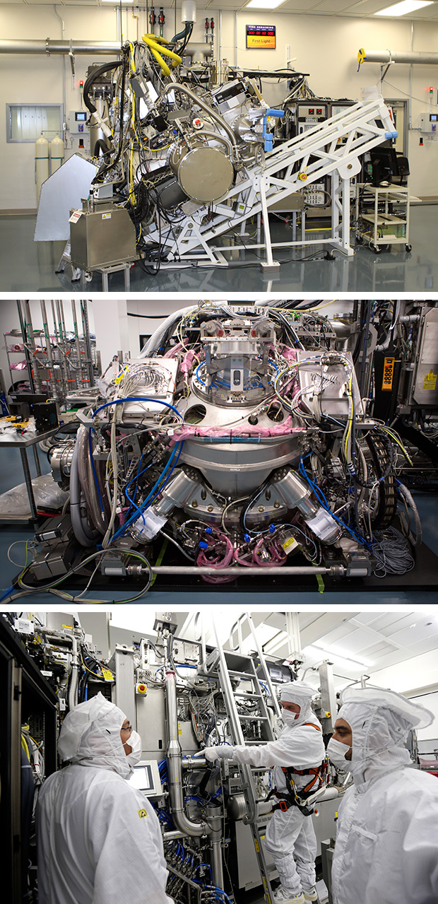
EUVL scanner. Instead of lenses used a set of mirrors.
But the creation of EUV-systems, bright enough and reliable, working in a factory for almost 24 hours a day, 365 days a year, turned out to be incredibly difficult from an engineering point of view. For many years, EUV was treated with skepticism, and it did not meet expectations many times.
But now it is actually transforming the industry. The brightness of the source, made by the Dutch company ASML Holding, is close to sufficient for commercial use. ASML supplies EUV scanners that will be ready for mass production of ultra-modern microprocessors and memory as early as 2018. Advanced chip manufacturers are working hard to integrate these machines into their production lines.
The stakes are high. Moore's law faces serious difficulties, and no one knows how the semiconductor industry, which earned $ 330 billion last year, will behave in the next 5-10 years, or how it will look when Moore’s law ends. Reduced revenue may be inevitable. But if the pursuit of the law allows, say, to avoid a 15% drop in profits, this will mean that the industry has retained a profit that is twice as large as the income of the entire US gaming industry.
The detail of the technology depends on several factors. One of the main ways to achieve improvements is to shorten the wavelength of the light used. For decades, lithographers have been doing this, shifting their cars from the blue part of the visible spectrum down to shorter UV waves.

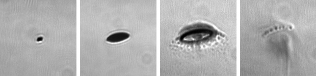
On the left - modern technology at 193 nm using multipatterning, on the right - promises of EUV technology. The lines on the micrographs have a minimum width of 24 nm.
In the late 1980s, the semiconductor industry began to move from mercury lamps to lasers, reducing the wavelength from 365 nm to 248 nm . Some researchers already planned a larger leap into the x-ray region. Hiro Kinoshita [Hiroo Kinoshita], who worked for the Japanese telecommunications company NTT in 1986, reported on the results of work on his idea using 11 nm radiation. Others at AT & T Bell Laboratories and Lawrence Livermore State Laboratory also independently worked on the technology. In 1989, some researchers met and exchanged their knowledge at a conference. In the following years, industry and government players were invested in the research.
ASML with several partners began work on EUVL in the late 1990s. Then Anton van Dijsseldonk [Anton van Dijsseldonk], who grew up in the Netherlands town of Veldhoven, where ASML is headquartered, became the first company employee working on the project. “They predicted the end of Moore’s law,” he recalls, and the semiconductor industry was looking for ways not to stop increasing the working permit in production. Chip makers tried to improve layering - the ability to repeatedly place the substrate in the scanner and print a new set of masks exactly at the right place. “People at the time were looking for alternatives,” says van Dieisseldonk, “and EUV was an exotic [technology].”
But from the very beginning, researchers from ASML were convinced that they could make technology work — and that it would be the most profitable method for manufacturers. Less than 10 years later, the company has already decided to build demonstration scanners that other researchers could use to test the technology.
But in the way of engineers who are trying to shine through the masks with the help of X-rays, physics gets up. At 13.5 nm, light is absorbed by a variety of materials. Even the air is “completely black,” and absorbs all the radiation, as van Dijseldonk says. So, they and their colleagues almost immediately realized that the scanner could work only in a vacuum, and each substrate should go in and out of it through the airlock.
There is also the problem of radiation deviation. EUV is absorbed by the glass, so it was necessary to abandon the lenses in favor of the mirrors. And not simple - the first polished surface that appeared would not have the necessary reflectivity. They had to use Bragg reflectors - multi-layered mirrors that collect several reflections into one fairly strong.


The scanner is being prepared for shipment to the customer. The machine is disassembled into nine parts.
Today, mirrors in EUV machines consist of 40 pairs of intermittent silicon and molybdenum, and each layer is only a few nanometers thick. Zeiss, which developed mirrors, makes them with high precision. But in the end, as Van Dieisseldonk says, “if you do this task unrealistically well, you will get a mirror with 70% reflectivity.” This means that each pair of system mirrors halves the radiation. The scanner may also need a dozen mirrors to redirect light from the source to the mask, which itself is also a mirror, and then to the substrate. After passing the path from the initial light can be only 2%.
The less light comes, the longer the substrate needs to remain in the scanner. At the factory time = money. For commercial use, the technology must compete in value with existing lithography techniques. The reflection loss must be compensated for by the high brightness of the light source. And it turned out to be very difficult to do.
Previously, researchers have already invented everything that can emit X-rays, including lasers and particle accelerators. But the method chosen as a result, which allowed achieving sufficient brightness in the most economical way, involves the use of plasma. If you subject the desired material to a sufficiently powerful laser or an electric current, you can separate the electrons from the atoms. The resulting plasma will emit EUV, and the heated matter will cool.
When using plasma, where the light from the source enters the scanner, its power is 250 watts. This amount of light will allow the machine to process about 125 substrates per hour. This number is at the level of the desired quantity for mass production, and less than two times compared with modern machines operating from 193 nm.
But for many years, progress was slow, and the increase in the brightness of the light did not reach the predicted. By 2011, five years after the appearance of the first test scanners from ASML, one of the leading developers of light sources, Cymer was able to create a source that issued 11 watts on an ongoing basis. “We underestimated the difficulties involved in this task,” says Hans Meiling, responsible for marketing at ASML. As a result, ASML bought Cymer for € 3.1 billion in 2013.
To create a source of EUV Cymer use plasma, obtained by means of a laser. 50,000 microscopic drops of ultrapure tin per second rush through the vacuum chamber, and each of them is illuminated by the light of a carbon dioxide laser that has passed through several amplifiers, originally designed for metal cutting. When a laser pulse encounters a drop, it heats up to a plasma state and emits an EUV. The collecting mirror reflects the light and sends it to the scanner. So that tin residues do not accumulate on the mirror, it is constantly flushed with hydrogen.
“When I first heard about this, I decided that this was some kind of madness,” admits Alberto Pirati, who joined the development of the EUV source in 2013. But little by little the team has reached almost impossible. One of the breakthroughs happened thanks to the technology studied in Cymer before the acquisition. They found that if a preliminary pulse was given before the main laser, each drop of tin would flatten out into a disk, and thus the surface area would increase to interact with the main laser pulse. This technology has increased the conversion yield from plasma to EUV from 1% to 5%. Thanks to her and other optimizations, the company announced in the beginning of the year that it reached 200 watts of power. Another light source developer, Gigaphoton, also reported great progress. The long-awaited 250W power source is just around the corner. For real technology tests for its readiness for mass production will occur in the laboratories of ASML customers.
No one doubts that EUV machines are capable of great detail. At the conference on semiconductors, you will surely see a presentation with microphotographs of EUV masks and a comparison with blurred masks obtained by existing methods.
The question is what role will EUV play in mass production - and when. The cost of switching to it depresses. The price of the new unit from ASML exceeds € 100 million, which is twice as expensive as the scanner at 193 nm. It competes in size with the bus, and requires several flights of 747 for delivery. It can consume about 1.5 MW, which is much more than a machine at 193 nm.
Evolution of a drop of tin. The first impulse flattens, the second transforms into a plasma.
But a simple comparison of specifications does not reflect the full cost of production. Today's lithographic systems at 193 nm can produce chips with dimensions of several fractions of this wavelength. This was made possible thanks to two breakthroughs. The first is immersion lithography , which places water between the silicon substrate and the projecting optics. The second is multipatterning , which breaks up the process of creating a layer into several steps. For example, to create several closely spaced holes, the substrate can first be driven through the scanner, which creates half of the holes, and then a second time - to create the second half with a slight shift. Since the location of the substrate is determined with high accuracy, engineers can create properties that are impossible in a single pass. And the more steps are used, the finer the details can be. But each step complicates and increases the cost of the production process.
Now GlobalFoundries uses triple pattering for making 14 nm chips, and the most advanced ones are created in Fab 8. This means that for critical layers the chip has to make two additional passes through the scanner, and all the other tools that create layers. The company intends to switch to quadruple pattering with 7 nm details - this is what George Gomba, a technology assessment project leader, says.
So far, GlobalFoundries expects to roll out technology at 7 nm by 2018 without using EUV, but when the latter reaches readiness, it will not give up on it. The key question is when the value of EUV equals at least with multipatterning. It is difficult to answer it, because the answer depends on several unknown factors, including the brightness of EUV sources and the possibility of continuous operation of the whole technology based on EUV.
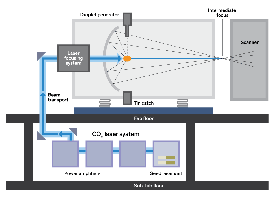
Schematic diagram of the light source
But not only GlobalFoundries and IBM are investing in EUV. In 2012, Intel, Samsung and Taiwanese manufacturer Taiwan Semiconductor Manufacturing Co. (TSMC) invested a total of € 1.38 billion in new-generation lithography research conducted by ASML (at the same time, the company collected € 3.85 through shares). Meiling says that the company employs about 4,000 people, not counting researchers working at the largest chip makers and research institutes working independently on technology.
All these investments occur not only because EUV technology is complicated, but also because manufacturers understand that soon they will not be able to move on without it. Anthony Yen, leading the development of EUV-lithography at TSMC, speaks directly about the criticality of EUV to fulfill Moore's law: “Critical at 100%. Very, very critical. ” TSMC experts are going to start using EUV in 2020, when the company will begin manufacturing 5nm chips.
There are still technological difficulties. In the first rows - protection of the mask, the surface of the stencil, which will be printed on the substrate. Here again the question of reflectivity arises.
In the machine, working on technology 193 nm, the mask is protected by a film called pellicle, which is stretched at a short distance from it in the manner of packaging. With current technology, a speck of dust, invisible to the eye, falling on a stencil can kill hundreds of transistors. But if it falls on the pellicle, it will be out of focus and will not prevent the creation of a pattern on the substrate.
But these pellicle are not transparent to 13.5 nm light. ASML wanted to build scanners without films, but manufacturers are stopped by the drawbacks of this approach. “If one particle gets on the mask,” says Yen, “then all the substrates will be damaged. In general, you can stay with zero output. " Months of work, and tens and hundreds of thousands of dollars are wasted.
Therefore, ASML is investigating the issue of the manufacture of pellicle, which is able to withstand EUV radiation. And it must be transparent, which is even more difficult. Since the EUV masks are not transparent, but reflecting, the light must pass through the pellicle twice - inside and outside.
There are other difficulties that potential customers face. For example, it is necessary to find the ability to make masks without defects, as well as the ability to verify the absence of defects in masks. Or photoresist - a photosensitive layer covering the substrate, copying the pattern from the stencil.
Modern chemically enhanced resists are made of polymer chains of molecules that multiply the effect of incoming photons. But these materials are notoriously absorbing EUV, as explained by Andrew Grenville [Andrew Grenville], CEO of EUV-resist startups, Inpria. Moreover, the captured image is slightly blurred as the light amplification reaction penetrates the material. For making sharp contours, “smaller and more stable components are needed,” says Grenville. Inpria works on a resist of small tin oxide components that absorb EUV five times better and create patterns without amplification.
Will the engineers have time to support Moore's law, for a while or forever? Chris Mack, an expert in lithography, doubts that all the pieces of the puzzle can be assembled by 2018. Planning for the production of new-generation chips requires several years. It is very risky to give a pledge to use EUV technology in the next few years, he said.
, EUV, Lotus Elise, , . . , , . EUV, : « , EUV ».
, . EUV , , , . , , , – , . , : «, , ».
, , , . , . .
Source: https://habr.com/ru/post/398967/
All Articles