Scientists of NITU "MISiS" were the first in the world to study a new one-dimensional semiconductor material
Using the method of micromechanical splitting, with the use of which graphene was discovered at one time, for the first time in the world, a new one-dimensional semiconductor material was obtained from the synthetic material Ta-Pd (Pt) -Se. Its use in microelectronics will reduce the electronic circuits to nanoscale and increase the speed of the devices. The theoretical part of the study was carried out by scientists of the Inorganic Nanomaterials Laboratory of the Theoretical Materials Science of Nanostructures Infrastructure at NITU MISiS under the guidance of Pavel Sorokin, Doctor of Physics and Mathematics. The experimental part of the work was carried out by American colleagues at the University of Tulane under the guidance of Professor Jiang Wei. The results of a unique study published in the journal Nano Letters .
The task of obtaining a one-dimensional semiconductor has been for scientists for quite some time. The creation of such a material, the main field of application of which is opto- and microelectronics, would increase the speed and reduce power consumption of the devices. Reducing the size of materials often allows for extraordinary electronic, optical, mechanical, chemical and biological properties due to dimensional and surface effects.
Intensive research in this direction began in 1991, when the hexagonal structure of carbon nanotubes was identified, which made it possible to speak about a new class of one-dimensional nanomaterials that have a future use in nanoelectronics. After receiving graphene in 2004, attempts were made to cut it by making a one-dimensional semiconductor nanomaterial out of it, however, the sensitivity of the conductive properties of the obtained tapes to the width and structure of the edges does not allow us to speak about their perspective in electronics. Attempts to obtain tapes from two-dimensional semiconductors - transition metal dichalcogenides were also unsuccessful, since they consist of three interconnected chemical atomic layers, which turned out to be very difficult to cut into high-quality tapes.
Since the traditional method — cutting two-dimensional materials — did not succeed in obtaining one-dimensional semiconductors, the scientific collaboration between research teams of NUST MISiS and Tulane University approached the problem from a fundamentally different side. It was decided to look for a crystal consisting of weakly bound one-dimensional nanostructures (as in the case of graphite consisting of graphene sheets) in order to apply the same method of micromechanical splitting (the method of "adhesive tape") to it.
')
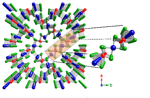
This material was Ta 2 Pt 3 Se 8 (tantalum-platinum-selenium) and Ta 2 Pd 3 Se 8 (tantalum-palladium-selenium), synthesized more than 30 years ago, but still not widely used. It has a very interesting structure: it can be represented as loosely interconnected nanometer-wide tapes.
According to the head of the research group, Pavel Sorokin ,
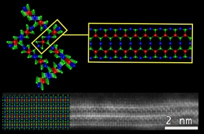
Experiments with Ta-Pd (Pt) -Se crystals were carried out by an American group of scientists. In the NITU "MISIS" in parallel was carried out theoretical work. The results of experimental studies, including the data of transmission electron microscopy, perfectly coincided with the theoretical results. The splitting of Ta-Pd (Pt) -Se made it possible to obtain nanowires consisting of several nanoribbons that have a direct band gap of about 1 electron volt (eV). The researchers created a transistor based on the nanostructures obtained, in which the experimentally measured charge carrier mobility was 80 cm 2 B -1 s -1
As noted by the rector of NITU "MISIS" Alevtina Chernikova ,
The task of obtaining a one-dimensional semiconductor has been for scientists for quite some time. The creation of such a material, the main field of application of which is opto- and microelectronics, would increase the speed and reduce power consumption of the devices. Reducing the size of materials often allows for extraordinary electronic, optical, mechanical, chemical and biological properties due to dimensional and surface effects.
Intensive research in this direction began in 1991, when the hexagonal structure of carbon nanotubes was identified, which made it possible to speak about a new class of one-dimensional nanomaterials that have a future use in nanoelectronics. After receiving graphene in 2004, attempts were made to cut it by making a one-dimensional semiconductor nanomaterial out of it, however, the sensitivity of the conductive properties of the obtained tapes to the width and structure of the edges does not allow us to speak about their perspective in electronics. Attempts to obtain tapes from two-dimensional semiconductors - transition metal dichalcogenides were also unsuccessful, since they consist of three interconnected chemical atomic layers, which turned out to be very difficult to cut into high-quality tapes.
Since the traditional method — cutting two-dimensional materials — did not succeed in obtaining one-dimensional semiconductors, the scientific collaboration between research teams of NUST MISiS and Tulane University approached the problem from a fundamentally different side. It was decided to look for a crystal consisting of weakly bound one-dimensional nanostructures (as in the case of graphite consisting of graphene sheets) in order to apply the same method of micromechanical splitting (the method of "adhesive tape") to it.
')
This material was Ta 2 Pt 3 Se 8 (tantalum-platinum-selenium) and Ta 2 Pd 3 Se 8 (tantalum-palladium-selenium), synthesized more than 30 years ago, but still not widely used. It has a very interesting structure: it can be represented as loosely interconnected nanometer-wide tapes.
According to the head of the research group, Pavel Sorokin ,
“The uniqueness of our work in its novelty - we showed that to get the desired result, we need to look at the task from a different angle: not to try to cut the existing material, but to look back and find another one that has a suitable atomic structure. To solve our problem, the nanostructures of the composition Ta-Pd-Se and Ta-Pt-Se ideally suited, in which, I believe, we will find in it many more interesting properties ”.
2.1 nm Ta-Pd-Se nanowire - experimental image and theoretical model. The frame highlights the structure of the structure - a separate Ta 2 Pd 3 Se 8 nanoribbon
Experiments with Ta-Pd (Pt) -Se crystals were carried out by an American group of scientists. In the NITU "MISIS" in parallel was carried out theoretical work. The results of experimental studies, including the data of transmission electron microscopy, perfectly coincided with the theoretical results. The splitting of Ta-Pd (Pt) -Se made it possible to obtain nanowires consisting of several nanoribbons that have a direct band gap of about 1 electron volt (eV). The researchers created a transistor based on the nanostructures obtained, in which the experimentally measured charge carrier mobility was 80 cm 2 B -1 s -1
As noted by the rector of NITU "MISIS" Alevtina Chernikova ,
Pavel Sorokin, Head of the Project “Theoretical Materials Science of Nanostructures” in the Inorganic Nanomaterials Laboratory, Doctor of Physical and Mathematical Sciences, is the winner of an open international competition for receiving grants from NITU “MISiS” and one of the most promising young scientists of our university. For his scientific achievements, he was awarded the Scopus Award Russia 2015 Award in the Young Scientist category.
Source: https://habr.com/ru/post/397213/
All Articles