IBM and Samsung have developed 11 nm memory STTMRAM

This month, IBM celebrated the 20th anniversary of the random access magnetoresistive memory (MRAM) project . Initially, the goal was to control the cell using an electromagnetic field. Now the project has been transformed into the development of a memory cell with the recording of information through the transmission of spin torque by an electron. This type of memory is called STTMRAM (spin-transfertorqueMRAM).
Together with IBM, many partners worked on this project. The first was Motorola. Then - Infineon, TDK, Micron and others. Thanks to the participation of specialists from these companies, the project was transformed from a purely theoretical concept into a real technology. For several years, a number of technical problems made it difficult to scale the memory to high density. But this problem was still solved. And now we, together with Samsung, have reached the final stage. We can say that the development is already close to a commercial launch. Now the main task is solved, experts optimize the main technology and auxiliary tools. The main achievement of work with Samsung was the transfer of the cell structure from horizontal to vertical.
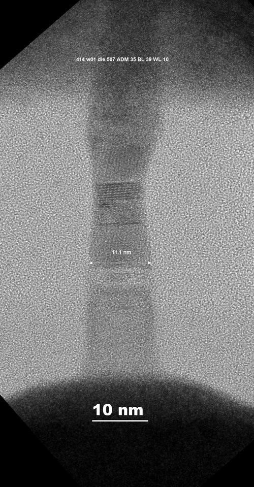
A test sample of STTMRAM memory is now ready. The size of the working part of the cell is 11 nm. Accordingly, the memory of this type will be made on the 10-nm process technology. Cell access speed is about 10 ns. By this parameter, the new memory is next to DRAM, not NAND flash. STTMRAM is positioned as main memory with a virtually infinite resource for rewriting.
')
Another advantage of the new product is its lower power consumption compared to traditional memory types - only 7.5 µA is required for recording.
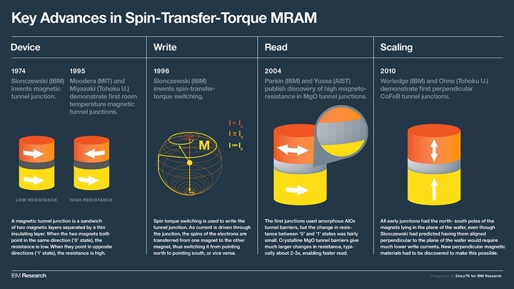
Spin moment transfer technology (spin-torque-transfer-STT) or spin transfer switching uses electrons with a certain spin state (so-called polarized electrons). When passing through a ferromagnetic layer, these electrons change the intrinsic magnetic moment of the layer and reorient its magnetization ... This method reduces the amount of current needed to write data to the memory cell. Energy consumption in reading and writing becomes almost the same. In the case of traditional MRAM technology, with an increase in the density of memory cells, the current required for recording is also increased. The new technology will be relevant for technical process 65 nm and less.
 Magnetoresistive memory has approximately equal speed with SRAM and the same cell density. But the power consumption of MRAM is much lower than that of DRAM. In addition, as mentioned above, this memory does not degrade over time. Together, these properties of magnetoresistive memory make it truly universal. It can replace several types of memory at once, including SRAM, DRAM, EEPROM and Flash. This will lead to the unification of memory on different devices and in different types of drives.
“Due to its advantages, the MRAM chip can replace the combination of SRAM and flash-memory in some types of devices that work with not very demanding applications. But our long-term goal is to develop a SpinTorqueMRAM based solution for IBM servers, ”said Dr. Daniel Worledge, one of the leaders of the new type of memory development project at IBMResearch.
On November 7 of this year, our company holds a symposium dedicated to the 20th anniversary of the development of SpinTorque MRAM. The details of the event can be found at this link .
Source: https://habr.com/ru/post/396691/
All Articles