Reverse engineering laser scanner Leuze RS4
Earlier, I already talked about reverse engineering of a laser distance sensor . This time we will talk about a more complex device - laser scanner Leuze RS4. Like the sensor, this scanner came to me in a broken condition, so I had to rebuild its work, and in the process improve some of its characteristics, and, in fact, redo it into another device.
What is this laser scanner?
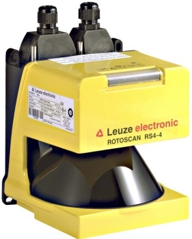
Leuze RS4 is a laser safety scanner, that is, it is designed to prevent people from entering dangerous areas in production, to prevent collisions of production vehicles, etc. It has quite decent characteristics - maximum range: 15 / 50m (depending on the operation mode ), the distance measurement accuracy in the whole measurement range is 5 mm, the angular resolution is 0.36 degrees, the scanning speed is 25 rev / sec (25000 measurements / sec).
It should be noted that this scanner is positioned precisely as a security device - that is, it stores in memory the location of alarm and warning zones, and if an object hits these zones, one of the keys opens in the scanner. To adjust the location of zones, the scanner can be connected to a computer and observe the location of obstacles on the screen. There is even a package for ROS that allows you to receive data from this scanner.
I got a scanner without a case, disassembled into its component parts. The scanner has failed due to a strong blow to the body; what exactly stopped working in it, I didn’t understand - perhaps the optics got misaligned, the contact went off in one of the connectors, or the encoder sensor moved, or something else. I tried to put all the parts together, I saw the scanner in the native software, but the scan did not start. So I only have one way to start it - to restore the scanner circuit as completely as possible, and to write my own microcontroller firmware.
Here are the parts that I had:
')
This is how they should be located in the case (a photo from the documentation, it is clear that the design and electronics are slightly different):

Also an important part of the scanner is the scanning mirror (highlighted in blue in the photo above), installed in its center:

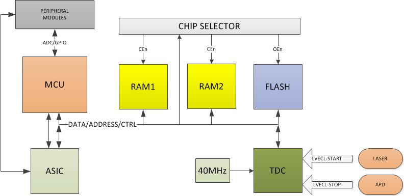
Scanner block diagram:

As can be seen from the diagram, the entire scanner electronics consists of separate modules (cards) connected by connectors and loops.
There are a lot of modules - power supply module (DC-DC), interface module, processor module, photodetector module (APD), laser module. In addition, there is also an encoder module and two horseshoe-shaped boards, which at first seemed strange.
First of all, it is worth paying attention to them:

Obviously, one of the boards contains LEDs, and the second - photodiodes. Initially, I thought it was some kind of encoder, or some kind of mechanism for checking laser radiation. However, later, after reading the documentation on the scanner, and having examined the photos in detail, I realized that this is a system for monitoring the condition of the protective glass surface of the scanner.
The photo shows the holes for the LEDs:
By measuring the level of the signal from the photodiodes, you can estimate the transmittance of the protective glass. Obviously, this system is not critical for the operation of the scanner, so I did not use these boards in the future.
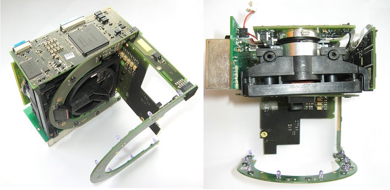
The processor module is the most difficult part of the scanner. It looks like the electronics of the module from two sides:

When I looked at the board for the first time, I immediately realized that the scanner uses the time-of-flight distance measurement (TOF) method - the chip with the largest marking turned out to be " ACAM TDC-GPX ", about which I had already heard before. TDC - “Time-to-Digital Converter”, that is, a specialized chip designed to measure time intervals with very high accuracy, and that is what they are used to measure the “flight” time of a laser pulse.
Also on the board was an Infineon C167 microcontroller with an external FLASH memory chip (which pleased us) and an ASIC (which was very distressing). In more detail about this module I will tell below.
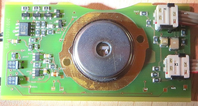
The power module contains some custom galvanically isolated DC-DC converter with several voltages at the output and several capacitors:
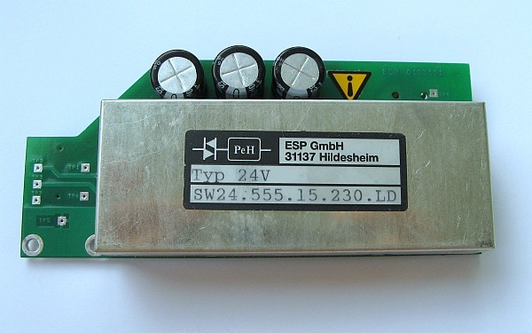
Converter supply voltage - 24V. Its main feature is that it outputs a high voltage (~ 230V) to a separate small connector, which is necessary for the operation of a laser and a photodetector.
It also outputs the following voltages to the main connector: + 5V, -5V, ~ 15V, galvanically isolated from the rest + 5V for the RS232 interface.
Optical part of the scanner
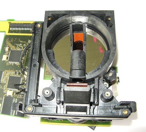
At first glance, the scanner optics is not very clear where that. In this case, a small window with a mirror in the center of the photo serves to output the laser beam, and the large shiny surface around it is the surface of the interference light filter installed in front of the lens of the photodetector. This light filter transmits only the radiation, the wavelength of which is close to the laser wavelength.
This is how it is shown in the scanner documentation:
The lens itself is installed inside a black plastic casing, so it’s problematic to see it. At the end of this casing, opposite to what is seen in the photo above, the laser and photodetector module is fixed:

Laser module
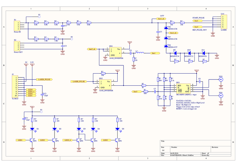
Type of laser module (some parts are marked by me in the process of drawing a scheme):
As you can see, the circuitry of this module is quite simple, so I was able to completely restore its circuit:
A large round detail on the board is a specialized laser emitter. Unfortunately, there were no markings on it, so no documentation was found for it.
From the description on the scanner you can find out - “Laser light wavelength - 905 nm”, “Laser class - 1”, “Pulse duration - 0.003 µs”, “Repetition frequency - 25 kHz”.
What was possible to understand by restoring the module circuit, and analyzing its work:
- The laser emitter is constantly supplied with a supply voltage of 143 V, limited by zener diodes.
- The emitter starts on the leading edge of the pulse supplied to the input "3" of the module. As I understand it, the pulse length can be arbitrary, the module itself will form a short pulse.
- The emitter contains a photo sensor, at the output of which a pulse appears at the moment when the laser actually turns on. The signal from it is used as a reference (starting pulse) when measuring the time of “flight”.
All control of the laser is carried out on one line - “LASER_PULSE”. Most of the time on the line should be "high" level. When a negative pulse is applied along its leading edge, the DD1 trigger is reset to 0, and on the rear pulse, the trigger begins to “wait” for the signal from the photodiode and the laser starts. When a signal from the photodiode appears, the trigger switches to 1.
You can see two coaxial wires, using connectors connected to the module. They are used to transmit the differential signal from the trigger to the TDC chip.
Also on this module are installed five LEDs. They are controlled by a processor module.
Photo receiver module
The module itself looks like this:

Photo of the photodetector near:

The sign of high voltage in the corner of the board clearly shows that an avalanche photodiode (APD) is used here - they need quite a high voltage to operate.
Unfortunately, there were no visible markings on the photodetector housing. By the emblem on the photodiode itself (in the center), it was only possible to determine that it was manufactured by Pacific Silicon Sensor (First Sensor) , but there was no further information about it, perhaps it is custom. It can be seen from the photo that this photodetector is a hybrid one, i.e. contains a built-in amplifier - it can be clearly seen above the photodiode. Obviously, the amplifier and the photodiode need power - it is supplied through the lower terminals (capacitors are soldered to them). The big mystery was the fine detail to the left of the photodiode, to which three conductors go. Further research has shown that this is an analog thermal sensor.
This module is much more complicated than the previous one. It uses a multilayer printed circuit board - at least 4 layers, with the majority of the signal lines located on the outer layer of the board, which greatly facilitates its analysis. In this module, I restored about 80% of the scheme, the rest I was not really needed.
The resulting circuit of the photodetector module:

At the top of the circuit is an adjustable linear high voltage source for an avalanche photodiode. It can generate a stable voltage of at least 150 V. This source is controlled by the DAC DA1 (LTC1451).
Since the scanner base is a pulse rangefinder, the main task of the photodetector module is to quickly detect a rather weak laser signal reflected from an obstacle. Since the level of the light signal is very small, it can only be detected using an avalanche photodiode, which has its own amplification. In this case, the signal from the photodiode is additionally amplified by an integrated amplifier integrated in the photodetector. Due to the fact that the amplifier is built into the body of the photodetector, the effect of interference on the useful signal is reduced. The signal generated by the photoreceiver (OUT_B) is transmitted to a certain DA4 chip, which, apparently, is another high-frequency amplifier. After it, the signal is transmitted to the direct input of the high-speed comparator D1 (MAX9601). A reference signal from a resistor divider (about 50 mV) is fed to the inverted input of this comparator.
The signal at the comparator output is differential, it is transmitted by coaxial wire directly to the processor module board.
In addition, the signal from the output of the amplifier DA4 is transmitted to some kind of peak detector, which "remembers" the maximum level of the received pulse. I did not restore the circuit of this node, and I drew on the diagram only its output stage (U1 chip), the signal from which is also transmitted to the processor module.
One of the least understandable parts of the scanner for me is the Q3 transistor mounted at the output of the RF amplifier. Judging by the circuit design, it is needed to enable the attenuation of the signal at the amplifier output. This transistor can be controlled by a signal from the processor board (line10 - “digi”).
You may notice that the board has an EEPROM chip. All signal outputs of this microcircuit are connected to the processor board. Apparently, in this microcircuit were stored some parameters, unique for each photodetector board, and recorded in it when testing the board. In particular, this may be the dependence of the APD amplification on the supply voltage, the dependence of the voltage at the output of the thermal sensor on its temperature, and other similar characteristics.
You can see that the power of the photodetector can be controlled by setting certain levels on the CLK, CS, CS2 lines associated with the DAC and EEPROM.
The board contains several circuits designed to monitor its condition. You can control the voltage level of the APD, its temperature (line7) and the threshold of the comparator. These voltages are converted by the operational amplifiers DA3-DA5 and transmitted to the processor module board.
Returning to the processor module
This module is the most complex of all, it contains a large number of multi-output chips, the printed circuit board is also four-layer, and most of the signal lines are divorced in the inner layers, which significantly complicates the restoration of the circuit.
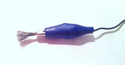
Very often it turned out that the tracks switched to the other side of the board. In order to quickly look for where a specific track is connected, I had to use just such a brush connected to a multimeter (which is in the dial mode):
I restored about 70% of the scheme - the rest I did not really need. Block diagram of the processor module:
The resulting processor module circuit:

Despite the fact that I call this module “processor module” everywhere, in reality, its basis is the Infineon microcontroller SAK-C167CR-L33M . It has 144 outputs, and is built according to the rather old architecture of the C166. This microcontroller does not have its own non-volatile memory - it is necessary to connect external memory to it via a parallel bus. In the scanner for this purpose, the flash memory chip M29F400B (512K x 8 / 256K x 16) is installed. Also, two microcircuits of RAM are connected to the microcontroller - IS61C6416AL-12 (64K x 16) and K6R4016C1D (256K x 16).
You can see that the address bus is connected to all memory chips with a shift in one bit - the memory A0 lines are connected to the A1 line of the microcontroller. This is due to the fact that addresses are set up on the address bus in bytes, but the controller and memory are 16-bit. In order for the controller to write single bytes into RAM without affecting the neighboring bytes in a 16-bit word, the memory chips have special lines UBn, LBn. Such a solution is very often found in devices with parallel buses and is described in detail in the documentation for the controller.
But the other solution in the processor module did not become completely clear to me. If you look at the flash memory chip U1, you will notice that the A14 line of the chip is connected to ground. The corresponding bus line address of the controller A15 is not connected to the microchip at all. The result is that the controller has access to only half of the flash memory. The situation with the RAM2 (DD3) microcircuit is completely the same.
The situation with the RAM1 (DD2) microcircuit is somewhat different - the controller A15 line is not connected to it either, but all the address inputs of this microcircuit are connected to the address bus, so the controller has access to the entire memory of the microcircuit.
And now you should pay attention to the node on the logical elements DX1, DX2, DD4. It is these chips that determine which memory chip is selected by the microcontroller. It can be seen that they are controlled by the following signals:
- WRn is the recording signal, the active level is low. On this line, the microcontroller sets a low level when you need to write some data to external RAM memory.
- A15 is the same data bus line that is not connected directly to any of the memory chips.
- CSn0 is a dedicated chip select signal, the active level is low. This line is connected to the address decoder built into the controller. After reset the controller is at a low level.
- RAM2_CE - connected to the GPIO controller with a pull to the ground.
The logic of this node is well described by the table:

As can be seen, depending on the state of the RAM2_CE line, the microcontroller will work either with Flash memory or with RAM2 (DD3) microcircuit, and their address spaces will coincide. It is worth noting that the memory capacity of these microcircuits is the same. Perhaps this is done to simplify the firmware update of the device. There is another option - the installed RAM works 3 times faster than the Flash memory, so after the start the controller can copy the contents of FLASH to RAM2, after which the program is executed from it.
But the high level on the A15 line clearly defines that the controller will work with a RAM (DD2) chip.
The result is that FLASH and RAM1 memory alternate in the address space of the controller:

Red indicates the area of RAM that has already been encountered - when accessing it, the controller will in reality get access to data located at addresses (0x8000-0xFFFF).
The compiler setting is not trivial, and, as I mentioned above, half of the Flash / RAM2 volume is lost. Why the developers of the scanner did not switch between FLASH and RAM chips using the dedicated CSnX controller line is not clear.
As I already mentioned, there is no flash memory in the controller used, which means there are no fuse bits. In order to adjust some parameters of the controller: the data bus width and addresses, the PLL parameters use pull-down resistors connected to the data bus. The controller itself has built-in pull-up resistors of high resistance (> 100 kΩ) connected to the entire bus. Thus, due to the external resistors on the bus, a certain combination of signals is established, which the controller reads when turned on. That it determines the desired settings of the controller.
In this case, we are talking about resistors R3-R6. The selected configuration of the resistors is consistent with the resulting bus signal connection circuit and provides the controller clock frequency of 33 MHz.
The pulse signal from the mirror encoder is fed to the input of the microcontroller timer “T2IN” through the logical element OR D6. The second input of this microcircuit is connected to the GPIO controller, which allows you to disable the supply of pulses to the timer input. Why do you need such a solution, and why you can not programmatically turn off the timer - I did not understand.
Now you should pay attention to the TDC chip (DD1).
The scanner is equipped with a TDC-GPX chip - the most “advanced” of all that is in the assortment of the company ACAM. The claimed measurement accuracy of time intervals is up to 10 ps RMS. The chip has 8 input channels of LVTTL lines and 2 channels of LVECL (differential).
In this scanner, in order to obtain the maximum time measurement accuracy, the LVECL inputs are used, to which signals from the laser module and the photodetector module are supplied using four coaxial cables. The signals from the laser module are fed to the DStart / DStartN inputs, and start the counting time. The signals from the photodetector module are fed to the inputs DStop1 / DStop1N, DStop2 / DStop2N, and stop the counting time. As can be seen from the diagram, stop signals are fed directly to two TDC channels, and with inverse polarity. Due to this, it is possible to measure not only the duration of the “flight” of a light pulse, but also the width of the received pulse.
TDC-GPX has a 28-bit data bus, but it can be switched to 16-bit mode, which is what is used in the scanner. The address bus is 4-bit, it is also shifted by 1 bit, like with memory chips. The microcircuits DD8, DD9, U2 are used to form the control signals of the microcircuit and the level matching - the microcontroller operates from 5V, and the TDC from 3.3V. In general, the TDC power system is quite complex, there is even an automatic adjustment of the supply voltage. Due to its complexity, I did not draw its scheme - I suspect that it is not much different from datasheet.
About programming the microcontroller and TDC, I will discuss further.
As I mentioned earlier, the board has a customized ASIC chip with the words "LEUZE98" and "WATCHDOG". What it is like is unknown. It is seen that a 20 MHz crystal oscillator is connected to this microcircuit. After I was able to program the microcontroller, I was convinced that the ASIC does not interfere with its operation, and did not restore the ASIC connection scheme. As far as I understand, this chip communicates with the controller via a parallel bus. It is possible that it is the ASIC that forms the RESETn reset signal, which resets the controller and the TDC.
However, with some chains had to deal more.
As it turned out, the laser control signal “LASER_PULSE” can be formed by both a microcontroller and an ASIC - using a node on transistors T1, T2. In this case, when turning on the ASIC opens the transistor T1, so that the controller is not able to control the laser. Because of this, I had to remove the resistor R24 - and the laser began to be controlled normally by the controller.
The mirror motor control signal “line_motor1” also came from the ASIC (via diode D2). Because of this, I had to cut the track and on the board and connect this signal directly to the free GPIO output of the controller - P3.15.
The strangest thing is that the “CS2” line connected to the DAC installed on the photodetector module board also turned out to be connected to the ASIC. Because of this, the controller could not independently set the APD supply voltage, and turn on the APD amplifier. Perhaps this is done to improve the reliability of the scanner - incorrectly adjusting the DAC can lead to failure of the APD. I also had to connect this line to the free GPIO output of the P3.4 controller.
It is precisely known that the three LEDs installed on the laser module are controlled by the ASIC. Two more LEDs that display the status of the scanner (the presence of an obstacle in the working area) are controlled from the controller by the LN1, LN2 lines. These lines also go to the interface module board.
Since the scanner can work in security systems, the processor board has a large number of nodes for diagnosing its state. The processor (and possibly the ASIC) can detect when the laser is turned on (using the U3 chip), monitor the level of several supply voltages, the APD supply voltage, the APD temperature, the comparator threshold on the photodetector board.
Due to the fact that the reference voltage of the ADC of the controller is 4.1V, part of the measured voltages is reduced with the help of resistor dividers - they can be seen in the diagram on the right.
And now it is worthwhile to examine in greater detail the method of generating an unusual “digi” signal, which I mentioned earlier when describing a photodetector module.
The diagram below shows the nodes simultaneously processor module (bottom) and the photodetector module (top):
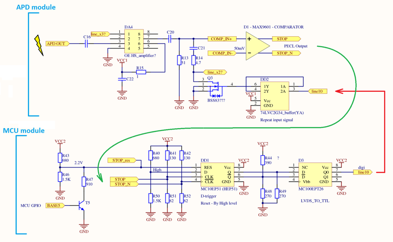
The arrows show the connection of the modules with the help of wires. Below I will describe the work of these nodes, as I understood it. In the photodetector module, the signal from the APD output is amplified by a DA4 chip, and then goes to the D1 comparator. If the signal level at the comparator input is greater than 50 mV, then the high level is set at the comparator output. The signal from the comparator output is transmitted to the processor module. First of all, it enters the TDC input, which counts the time from the start of the laser pulse. But in addition, this signal is fed to the clocking input of the D-flip-flop DD1. A logical unit is always supplied to the signal input of the trigger, and the trigger itself can be reset to the zero state using the GPIO line of the BASE5 controller. Thus, the triggering of the comparator triggers the trigger “1”. This trigger has a differential output, the signal from which is fed to the input of the D3 chip, which converts it to the LVTTL format. This signal is fed to the input «digi» of the photodetector module. As I mentioned earlier, in my opinion, the appearance of this signal leads to a weakening of the signal level at the input of the comparator.
The main question is why is it necessary and why is it so difficult to implement? Why it was impossible to make both nodes on the photodetector module board?
I can only express my assumptions. The signal may need to be attenuated in order to avoid the comparator or amplitude detector switching to saturation mode. Perhaps - to reduce the length of the received pulse. For both nodes simply could not find space on the photodetector board. Another option is possible - the signal needs to be attenuated only after it has time to reach the TDC via coaxial wires, which justifies such a complex structure.
The study showed that before starting a new laser pulse, it is necessary to reset the trigger, otherwise the pulses are not accepted.
Interface Module
Unfortunately, I did not have a good photo of this module. There is only this:

It is on this module that the only two connectors are installed to which you can connect outside the scanner. One of them is RS-232 / RS-422, the second is powered by the scanner, control signals are sent, and the safety circuit is connected here.
This module contains UART-RS232 / RS485 converters and optocouplers of optocouplers (they are installed on a separate small board shown on the right), safety circuit power switches, input circuits of the control lines for the rangefinder modes, an engine control circuit, an encoder signal converter.
This module connects the power module and the processor module, as well as the encoder module and the motor of the mirror (using the connectors on the bottom of the module, they are not visible in the photo).
Partial diagram of the interface module:
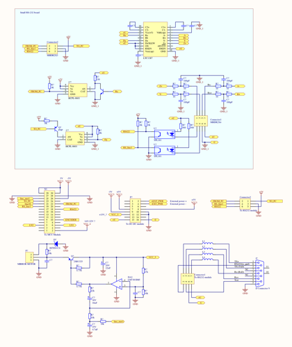
I recovered only a part of the scheme of this module (about 20%), since I was not interested in the keys and input lines needed for security. And there are quite a lot of them, the documentation mentions current limiting along the safety circuit, short-circuit control, and other functionality.
Somewhat strangely done control the speed of rotation of the motor of the mirror. Speed adjustment is implemented by changing the voltage of the motor power - with this all is clear. But the very adjustment of this voltage goes with the help of some kind of integrating chain on the operational amplifier. In order to increase the voltage, the controller sets 0 on the line “line_mot1” to lower it - 1. Obviously, without constant feedback from the encoder through the controller, the motor either stops or accelerates to maximum speed.
As it turned out, the UART-RS232 LTC1387 IC converter is rather slow - at a speed of 500 kbit / s, the data was distorted. Because of this, I had to remove a small board with this microcircuit, and connect the USB-UART converter directly to the interface module board.
Now, when I talked about the device of all modules, it is worthwhile to tell in more detail about the process of reverse engineering itself.
When I started to deal with the scanner electronics, most of all I was afraid that the impact could damage the laser or the photodetector. At the same time, I was not sure that I would be able to launch the processor module - they were confused by an unfamiliar microcontroller and ASIC. Therefore, the first thing I did was restore the circuit of the laser module and then the photodetector module. After I was able to figure out the circuitry of these modules and determine the purpose of all the contacts on their connectors, it was possible to proceed to the processor module. In the extreme case, if I could not start it, I had the idea to make an analog of this module on STM32 + TDC-GP2 microcircuits.
Obviously, to check the module, you need to run your own program on the Infineon SAK-C167CR microcontroller installed on it. Again, it is worth remembering that this controller does not have built-in flash memory. Moreover, as it turned out, the controller does not have any specialized debugging interfaces (including JTAG). With a high degree of probability, the firmware is recorded in an external Flash in the programmer in production. However, as it turned out, everything is not so bad - the controller has a bootloader (“Bootstrap Loader”), working on the UART. This bootloader is stored in the built-in Boot-ROM controller, so it definitely had to be in my controller. And it works in a rather peculiar way - to activate it at startup, you need to set the P0L.4 data bus line to a low level, after which the controller begins to wait for the 0x00 byte from the host to appear. Having received this byte, the loader automatically determines the transfer rate, and begins to wait for 32 bytes of data, which are copied into the controller's built-in RAM. After the data is received, the controller starts the execution of the received program (16 words of the controller).
In fact, one more boot loader (“preloader”) needs to be pushed into these 32 bytes, which the main loader “External loader” will receive from the host and will start its execution.
Then I was lucky - for this processor there is already a ready program FLASHit, which is able to do all the mentioned operations automatically. The loader built into it has quite a lot of functionality - with its help you can automatically determine the model of the installed Flash memory, edit and watch the contents of the controller registers, you can see the status of the ADC channels.
I did not manage to find on the board any test pads connected to the P0L.4 line of the controller, so in order to run the bootloader, I had to solder a special pin to this line. I stuck the pin itself to the case of one of the RAM microcircuits. To run the loader, you need to connect this pin through an 8 kΩ resistor to ground.
After I connected the board to the computer, and energized the processor module, the microcontroller actually showed up in FLASHit. After that, I wrote a small program in Keil that switches one of the controller's outputs, and wrote it in Flash. The program worked fine, ASIC did not interfere in any way (I was afraid of the work of some watchdog mechanism built into it, or conflicts on the tires), so that it was possible to move on.
After that, I restored the processor module circuit, which allowed to check the operation of all the modules in the collection.
First, I checked the operation of the laser module - as I wrote earlier, to launch a laser pulse, it was necessary to send only one signal to this module. The laser has earned - its flashes could be seen with the help of a mobile phone camera. Also, using an oscilloscope, I checked that the module normally generates starting (reference) pulses.
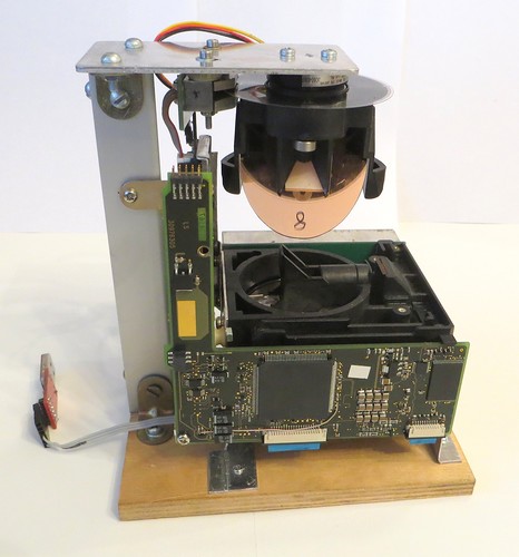
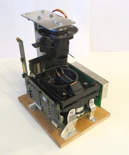
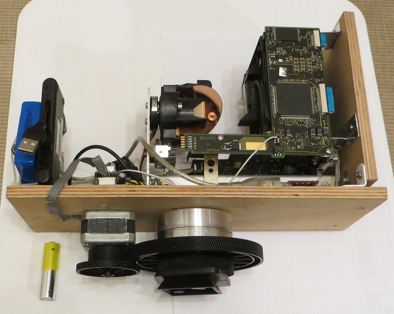
Next was the verification of the photodetector module. Then I had to check the operation of the DAC, the voltage shaping unit of the avalanche photodiode and the power control unit of the photodetector amplifier. They all earned, allowing you to check the work of the most rangefinder. To do this, I assembled its modules in the form as it was intended by the developers:

In the photo, all five main modules are assembled together around the optical system. Here, instead of a native rotating mirror, I installed an ordinary mirror.
After that, I filed wrote a laser control program for UART, set up the operation of the photodiode. As a result, when I started the laser at the input of the comparator, I was really able to detect pulses with an oscilloscope, the amplitude of which obviously depended on the type of obstacle in front of the mirror! The comparator also worked fine. There remained the last important part of testing - testing TDC.
The TDC-GPX chip installed in the scanner has a rather complicated construction and can operate in a large number of modes.
The figure below shows its structural diagram:

As you can see, the chip contains 8 separate channels, that is, it can receive up to 8 stop signals. If the channels are differential, then only two stop signals plus one start signal can be analyzed. In this case, the chip allows you to combine the measuring channels, thereby increasing the accuracy of measuring time intervals:

Honestly, I did not like the documentation for this microcircuit. Many things in it are described rather superficially, code examples are incomprehensible. The part of the datasheet dedicated to setting the time resolution is full of some kind of "magic numbers." There is also no normal “Application Note” on the microcircuit. In addition, in the scanner itself I was unable to detect the connections of the “EF1 / EF1” lines with the controller. As it is on these lines, one can determine that the microcircuit has finished measuring time. Because of all this, launching the TDC took me quite a lot of time, but as a result, everything worked as it should - when the laser was started, the TDC worked, and the results of the TDC operation clearly depended on the distance to the obstacle. Thus, the pulse laser rangefinder earned. It remains to turn the entire structure into a workable laser scanner.
The first step I needed was to make the adjustment - the assembled rangefinder stopped “seeing” the obstacles after a few meters. The optical system looked intact, but I had to remove the boards from the optical system, so the reflected light was not focused by the lens on the photodetector.
Before adjustment, I wrote a program for the controller, which not only determined the distances, but also measured using the ADC the signal amplitude generated by the peak detector.
The whole process of adjustment was reduced to smooth movements of the photodetector and laser boards, and the search for such a position at which the signal amplitude is maximum. As a result of the adjustment, the amplitude of the received signal was significantly improved.
Further, attention should be paid to a certain data processing feature inherent in pulse rangefinders.
The signal generated by the photodetector has an analog form.To convert it to digital form, which is further processed by the TDC, a comparator is used, which is configured to switch if the input signal exceeds a certain set threshold. As a result, due to the complex shape of the input signal, when changing the amplitude of the signal, an error occurs when determining the time intervals:

As can be seen from the graph, a signal with a smaller amplitude will be detected with a delay. To solve this problem, there are several methods, both hardware and software. I decided to use the simplest option - correction of measurement results depending on the amplitude of the signal. At the same time, I had to collect statistics on the change in the measurement results of time from the signal amplitude change. In order to change the amplitude of the signal without changing the rest of its parameters, I used paper lining on the lens, which reduced the luminous flux falling on the photodiode.
The result was the following dependence:
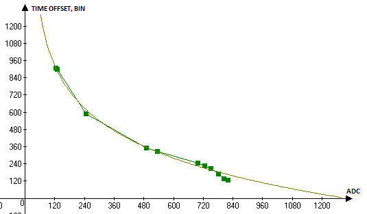
On the basis of this dependence, I formed a table of corrections, the data from which are used by the controller program when determining the distance to the object.
The next stage is the start of the engine mirror and encoder.
I have already quoted a photograph of a mirror:
The mirror motor is brushless, very similar to those used in cooler fans. Three wires go out of it - 2 of them are powered, another one is a pulse signal of speed. All these wires are connected to the interface module, while the speed signal generated by the engine is not used - control is based on data from the encoder.
As can be seen from the photo, a transparent disk with labels for the encoder is attached to the motor axis. You may notice that the disk has a zero mark.
The encoder was installed on a small board and completely covered by a metal screen, so its marking could not be determined. However, based on its size and pinout, I decided that it was a HEDS-9040 quadrature encoder:

Four wires went from the encoder board to the interface module, but as it turned out, only three of them were used - two power supplies and a signal.
As I understand it, the Schmitt triggers and some logic combining data from channels A, B, and index (zero mark signal) were installed on the board.
This is how the signal from the encoder board and the index signal taken directly from the encoder look like.
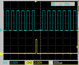
As you can see, during the index signal, encoder pulses are suppressed. As it turned out, the encoder board generated 500 pulses per revolution, but the timer of the T2 controller, to which the encoder line is connected, can be triggered simultaneously on both fronts of the pulses, which gives 1000 interrupts per mirror revolution. This value corresponds to the declared angular resolution of the scanner at 0.36 degrees.
I set up the T2 timer in the “Capture mode” mode, which allows me to measure the time between interrupts from the encoder. The resulting time is used to detect the "zero" position of the mirror, and stabilize the speed of rotation of the motor. At the same time, the number of interruptions is counted, which makes it possible to determine the position of the mirror.
After the encoder started working and I managed to start the engine speed control, I could fully assemble the scanner. Due to the complex shape of the boards and the optics, the design turned out to be rather arrogant: It was not easy to assemble such a design - the accuracy of the location of the individual parts is very important for the scanner. If the axis of the mirror would not coincide with the optical axis of the rangefinder part, this could lead to the fact that the scanning plane would turn out to be strongly curved or inclined.
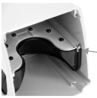
When measuring the exact distance to objects, it is important to have a certain “reference” object, the distance to which is precisely known. Knowing the "flight time" to him, you can accurately determine the time corresponding to the zero distance. Due to the change in temperature of the scanner components, this time may vary, so this time must be monitored continuously. To solve this problem, I installed a special blackened plate in the scanner:
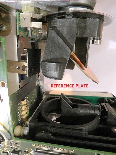
The plate is blackened so that the light reflected from it does not “blinded” the photodetector. Judging by the instructions, dark and light reflecting elements were also installed in the original design of the scanner. They were used to control the operation of the distance measuring part of the scanner, and most likely, they were also used for calibration.
In the photo above, the encoder mounted on the board is also clearly visible. As it turned out, the encoder must be very accurately set relative to the disk, and there were many problems with this - even a small offset of the encoder led to the loss of pulses, especially index ones. It is possible that the scanner stopped working after hitting the body because of problems with the encoder.
As a result, managed to get a scan speed of up to 20 revolutions per second. With an APD supply voltage of 135 V, distances up to 10–15 m normally go. At a voltage of 145 V and with additional filtering of the signal, distances can be measured up to 30 m (although I am not sure that it is safe for a photodetector).
It should be noted that the maximum transmission speed in the original scanner is 115200 bit / s, which allows you to transfer all data only at a speed of about 11 revolutions per second.
As I mentioned, in my firmware I transmit data at a speed of 500 kbit / s, which allows us to significantly increase the number of scans transmitted per second. It is because of the UART speed limit that I did not increase the scan speed to the original 25 revolutions per second. I note that in the original design of the scanner, the data is processed in the scanner itself, so that the low data transfer rate does not really affect anything.
Since the scanner is now working without a case, it was possible to increase the scanning area to 208 degrees against 190 in the original design.
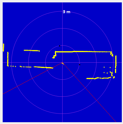
Visualization of data received from the scanner:
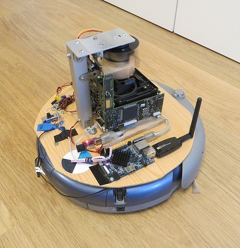
Obviously, the scanner should perform some useful function, so I decided to test its operation in ROS in SLAM, and compare the results with the results of a homemade laser scanner . For this, I installed it on Roomba, on which a homemade scanner was previously installed.
View of the Leuze scanner installed on Roomba (the mirror rotates so that it came out blurry): As a result of hector_slam, we managed to get such an apartment map (the walls are yellow): Since the vacuum cleaner travels at the floor level, it “sees” mostly furniture. But such a card is obtained if the vacuum cleaner is simply carried in the hands at the belt level: In this case, the apartment walls are “seen” more often.
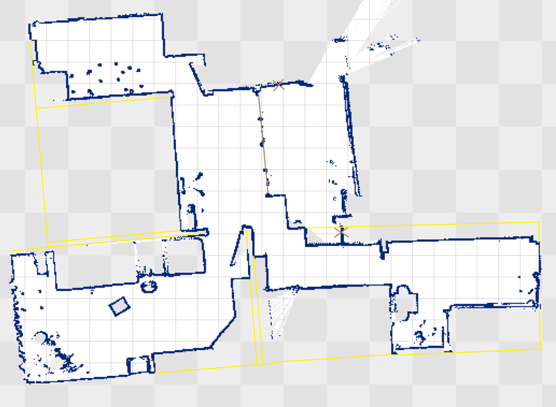
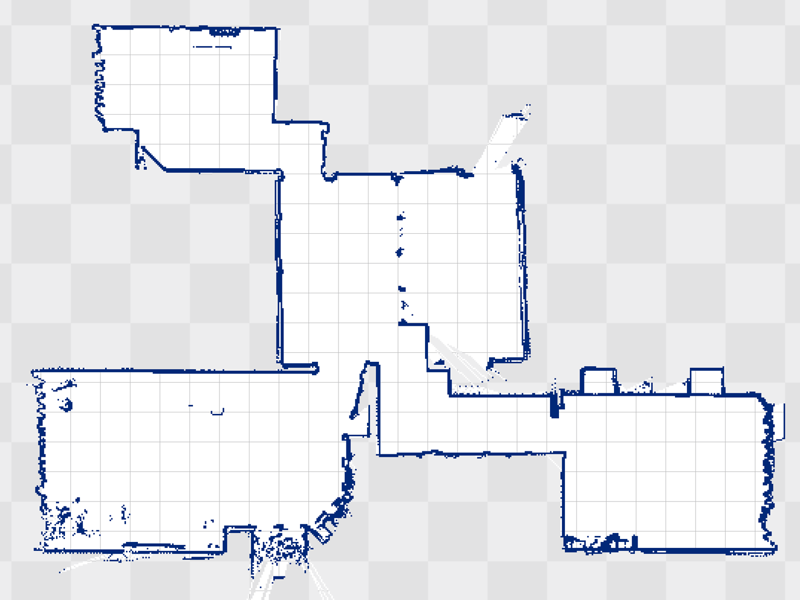
If you compare the quality of the cards, you can see that the homemade scanner has more “noisy” lines. This is due to the fact that the homemade scanner that uses the triangulation principle of operation, with increasing distance greatly decreases the accuracy.
Unfortunately, despite the very good quality of scanning, this scanner is poorly suited for an autonomous robot - it has too large dimensions and power consumption (about 7.2 W).
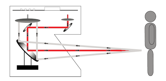
Where else can you apply such a scanner? Earlier, when discussing a homemade scanner, I was often asked about the possibility of making a 3D scanner, and it’s time to make it! There is a rather high scanning speed. Of course, by resolution such a scanner cannot be compared with scanners that use the triangulation principle of distance measurement (with a laser line or a projector (SLS)), but they can scan large spaces - rooms, street sections.
In order to remake a 2D scanner in 3D, you need to ensure that it can rotate along one more axis. I decided to make my scanner using the same beam sweep principle as in the scanner of thisarticles. For this purpose, I placed the Leuze scanner “lying down”, so that its scanning plane is perpendicular to the floor. Next, it was necessary to implement a smooth slow rotation of the entire scanner around the axis. The main difficulty - the scanner must rotate without beats and distortions, which will lead to the distortion of scans. As it turned out, at home it is difficult to make a bearing unit capable of providing such an exact rotation. Therefore, I decided to use the head of a VHS tape recorder as a bearing unit - it contains two bearings, is made with very high accuracy and is able to withstand the weight of the scanner. The resulting design is driven by a stepper motor.
The assembled 3D scanner looks like this: Type of scanner mounted on a tripod:
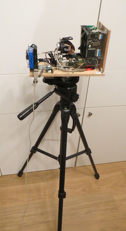
On the left there is a 12 V battery, which is also a counterweight. Since the Leuze scanner requires 24 V to work, I had to install on the scanner a step-up DC / DC converter assembled on the basis of the XL6009 chip. Stepper motor scanner is controlled by the module on the A4988 and Arduino, which provides rotation at a given speed. Both the Leuze scanner (via the USB-UART adapter) and the Arduino are connected via a USB hub with a wire to a computer that captures data. In the current view, the rotation of the scanner mirror and the rotation of the entire scanner are not synchronized - the scanner rotation speed is chosen such that when it is rotated by 0.36 degrees, the mirror has time to make at least three turns. Since there is no synchronization in speed, I had to transmit the positional sync information from the Arduino to the Leuze scanner.It is implemented quite simply - when turning the scanner for every 0.36 degrees, the Arduino changes the signal level at one of the conclusions. This signal is transmitted to the scanner processor module (to the unused connector of the protective glass status sensor). Information about the state of this signal is transmitted at the beginning of each scanner parcel - in this way, a self-written PC program controlling the scanner receives information about the movement of the scanner and determines the angle to which it is rotated.obtains information about the movement of the scanner and determines the angle to which it is rotated.obtains information about the movement of the scanner and determines the angle to which it is rotated.
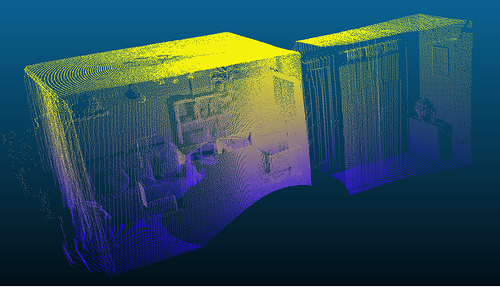
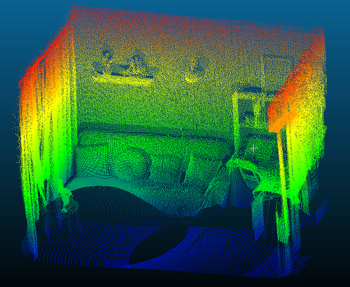
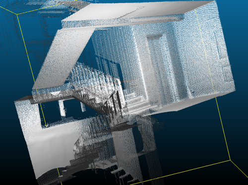
A single 3D scan formed by the scanner contains about 350'000 points. Of course, this is significantly less than that of professional scanners, but still pretty good, especially if you glue together a few scans together.
Example - single scan of a room: Example - scan of a room glued together from several: Scanned part of the entrance: Video, which shows the results of the resulting scanner:
→ Source code of the controller program on Github
Source: https://habr.com/ru/post/396357/
All Articles