Printed Circuit Trace in KiCAD
Introduction
One of the criticisms to the previous article was the following: they say to be so, shoot from a cannon on sparrows and even proprietary software for $ 10,000, besides, probably stolen from torrents. Leaving behind the moral side of the issue, as well as the presumption of innocence, we turn to the next question - and what do we have there in the Open Source sector, suitable for solving problems of designing electronic equipment. In particular, the manufacture of printed circuit boards. The most worthy, in my opinion, was the cross-platform program KiCAD , distributed under the GNU GPL license. There are versions for Linux, Windows and macOS.
')
Let us consider this tool in more detail with reference to the task I have already solved - tracing the printed circuit board for the level converter based on MAX232.
1. Installing KiCAD and Libraries
The distribution of the program and installation instructions are available on its official website . Since I prefer to use Linux, specifically Arch Linux, the installation is reduced to a spell for the package manager.
$ sudo pacman -S kicad kicad-library kicad-library-3d The first package is the program itself, the second is the library of components, the third is the 3D models of the components. Actually that's all. A similar set of packages is available for all popular Linux distributions. For Windows, download the binary installer here . For macOS, everything is the same . In general, the installation is elementary and does not cause difficulties.
2. Draw a schematic diagram
Running KiCAD we will see the main window of the program. It contains a project tree and buttons for invoking software components intended for various stages of device design.

Go to the menu File -> New Project -> New Project. We will be offered to choose a place where the project files will be located, as well as to choose its name. All files related to the project should be located in a separate directory. I have everything in the ~ / work / kicad / rs232 directory, and the project will be called rs232.
After creating a project, two files are generated in the tree: rs232.pro - project file; rs232.sch is a schematic file. Double click on the schema file and go to Eeschema - a program for drawing diagrams

The format of the main inscription of the drawing, of course bourgeois. But we are not interested in following GOST and ESKD. We need to evaluate the capabilities of the package to solve a specific practical problem, the path is even so simple. Therefore we will start drawing the scheme.
On the right side of the window is a toolbar. It has a button with the image of the operational amplifier - click on it and go into the component placement mode. By clicking the mouse in the field of the scheme we initiate the appearance of a dialogue

In the filter string, we start typing "max232". the system searches through the library and offers us the chip of interest. Select it, click OK and place the component in the right place in the schema with the mouse cursor. Similarly, we put on the circuit an electrolytic capacitor that responds to KiCAD called CP

We hover the cursor on the capacitor, press "V" and in the appeared window set its nominal

If you hover the cursor on any element, in particular the capacitor just added, you can perform the following actions by pressing the corresponding keys
M - move component (start moving)
C - create a copy of the component
R - rotate component clockwise
X - to reflect the component relative to the horizontal axis
Y - reflect the component relative to the vertical axis
Acting in the manner described, we place all the other components of the circuit. We will need the following items
| Name components in the library | Component type | amount |
|---|---|---|
| CP | Electrolytic capacitor | four |
| D | Diode | one |
| DB9 | DB-9 type connector | one |
| CONN_01x05 | Single row pin connector (5-pin) | one |
In addition, we need land and power +5 V. These elements are added in the mode of placement of power ports, which is turned on in the right panel with the button with the symbol of "earth". We will need the following ports: GND - the actual "land"; + 5V - no comment.
In the end, on the circuit field, we get something like this.

Now, by pressing the button with the image of the green line, we switch to the “Place Explorer” mode and connect the outputs of all elements according to the device’s schematic diagram. If we need an additional "ground", move the cursor to the nearest "ground", press "C" and clone it, without departing from the process of connecting elements. In the end, we get the following scheme

We draw attention to the fact that the elements of the scheme are not numbered. For this purpose, it is convenient to use the function of numbering elements. Call it either from the Tools menu -> Mark Scheme, or by clicking the Mark Label Components button on the top toolbar. We’ll be shown a dialog with item naming settings.

We set the settings we are interested in and click "Mark components". Now another thing

Assuming that we have completed the scheme, we check the correctness of its construction from the point of view of the rules of KiCAD. To do this, click on the top panel button with the image of a ladybug with a green check mark. In the window offered to us, click the “Run” button and get the result

There are no errors, but there are 13 warnings. These warnings are fundamental - they indicate that some of the conclusions of the elements are not connected anywhere, and also that we have not energized the circuit.
We have a lot of unused conclusions. So that the system does not swear at us about them, we note these conclusions as unused. To do this, select the mode for specifying unused pins by pressing the “X” button with a slanting cross on the right panel, the so-called “Not connected” flag. Mark this flag all unused pins

The inputs of the second channel MAX232 (legs 8 and 10) are pulled up to the “ground” in order to guarantee zero voltage on them when the device is working.
After that we check the circuit again.

Great, just two warnings about unplugged power. In our case, the power is supplied from another device through the P1 pin socket, so the system should not indicate this using the virtual power port PWR_FLAG. We install this power port on the circuit and connect it to the + 5V power port, to the “ground” and wire going from the P1 connector to the diode, as shown in the figure

Thus, we indicate to the system on which lines the power is supplied to the circuit and the next test passes without errors and warnings. Save the finished circuit.
Now you should create a list of circuit circuits that will be used by us in the future. To do this, go to the menu Tools -> Create a list of chains, or click the corresponding button on the top panel. In the window that appears

select the format of the netlist for KiCad, set the file name of the rs232.net list and click the “Generate” button.
The scheme is ready and you can proceed to the next stage.
2. Binding of components and their seats
This stage reflects the feature of KiCAD - the component's circuit designation is untied from its seat and visual presentation. Before proceeding with the PCB layout, each component must be aligned with its footprint - a topological structure that essentially sets the size and location of the holes and / or contact pads on the board for mounting this component. This is done using the included CvPcb package. To launch it, go to Tools -> Assign Component Footprint. The system will think a little and give a window

The first column contains the list of available libraries. In the second column - the list of components presented in our scheme. In the third - a list of available seats. Say we need to decide on the form factor of the capacitor C1. We have Ether capacitors available for mounting into holes with diameters of 5 mm, height 11 mm and with a distance between the terminals of 2 mm. Well, choose the Capacitor_ThroughHole library (capacitors for mounting in the holes) in the first column, the capacitor C1 in the second column, and the seat C_Radial_D5_L11_P2 in the third column. Double click on the selected footprint to link it to the component. The selected footprint will appear to the right of the C1 capacitor, as shown in the figure above.
To check, we will look at the drawing of the footprint by clicking the button with the image of the chip under the magnifying glass on the top panel.

Clicking on the button in the browser window with the image of the chip, we will see a 3D model of the component

We are convinced that the chosen seat corresponds to the actual details that we have. In the same way we connect also other components. I got this list

I must say to find the right footprint from the habit is quite difficult. But I managed to do with standard libraries. In any case, the problem of the lack of the necessary details is solved by way of googling or self-production (but this is beyond the scope of the article).
Save the resulting list, close CvPcb, and regenerate the list of chains. Now everything is ready to proceed with the direct wiring of the board.
3. PCB layout
To do this, from the menu of the schematic editor Tools -> Layout Printer Circuit Board, run the Pcbnew tracer.

To set up trace rules, go to the “Design rules” menu and in the window

we set the width of the tracks, the gap between them, the diameter of the holes, the diameter of the drill in accordance with your technical capabilities. My settings are shown in the screenshot.
Next, you need to import the designed scheme. To do this, go to the menu Tools -> List of chains. In the window that appears, select the chain list file (our rs232.net formed in the previous step) and click on the button “Read the current chain list”

If we were not mistaken in the previous stages, the process will go without errors. We close the window and see that the components are located in the drawing window of the board.

Of course they all stuck together in a heap. And they will have to be taken to their designated places. Movement of components occurs with the same commands as in the schematic editor - we hover the cursor on the element and press “M”. If we want to move the component to the other side of the board, then in the transfer mode we press the "F" key. This should be done with the U1 chip, because it is located on the side of the tracks, due to the SMD design of the case.
Popytytev a little get something like that

We try to place the components so that the intersecting links are as small as possible. Now you can start tracing. Automatic tracing did not work out for me, maybe I didn’t fully understand its settings. For manual tracing, we will switch to the tracing mode by clicking on the “Track mode: autotrace” button on the top panel.
Right-click on the empty space of the working window and in the drop-down menu select "Select a working layer". In the window that appears, select the B.Cu layer (copper on the back of the board)

Hover the cursor on any pin and click "X". A track will appear, going from the selected pin to the current position of the cursor. We pull this track, fixing its intermediate points with single mouse clicks. Upon completion, at the last pin, double-click. If we don’t like the result, press Esc canceling the path we’ve taken. Other useful commands and their hot keys are available in the context menu, called by the right button at the moment of tracing.
I must say that the tracing process is intuitive and pretty soon we get the result

The yellow line on the screen shows the outline of the board. To draw it, go to the Edge.Cuts layer (the list of layers is located in the program window on the right) and with the Line or Polygon tool (the button with the image of the dotted line on the right toolbar) draw the outline of the board.
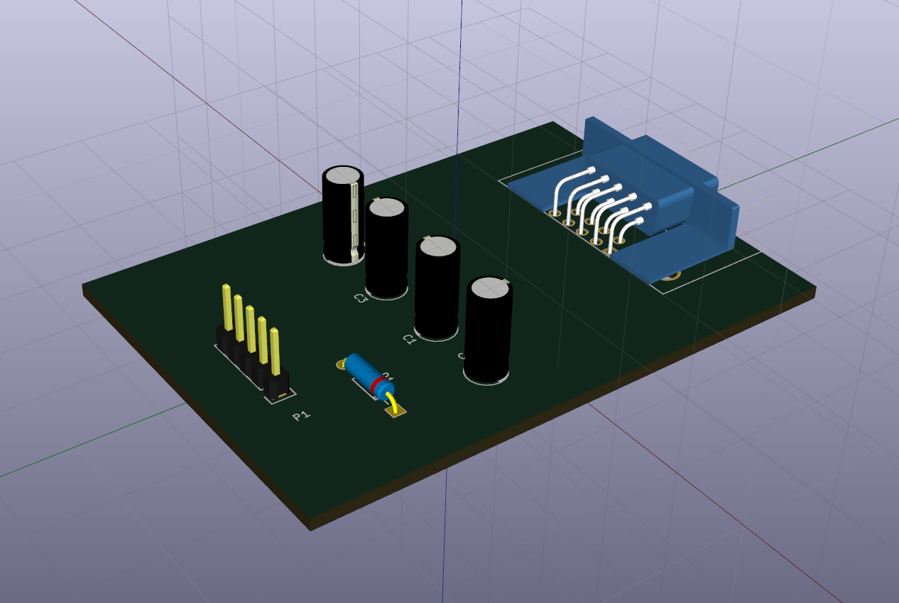
Now everything is ready. Save the result. You can view the resulting board in 3D mode (in the View -> 3D Viewer menu)


The result looks pretty nice, though the installation can be done and tight.
To get, for example, a template for LUT, go to the menu File -> Print. In the window that appears

Set the printed layer (B.Cu - copper on the back side of the board), be sure to tick the “Mirror” box, check that the 1: 1 scale is set and remove the “Print sheet frame” checkbox. Click print. If we do not have a printer, then we print in PDF

Getting the desired pattern

Conclusion
I must say that I quickly ran over KiCAD's capabilities, paying attention only to the key points of its use. This article is some introductory manual summarizing the very scattered information available on the web. Nevertheless, it can serve as a good start.
It can be concluded that the program is quite suitable for the design of printed circuit boards, given that the description of all its possibilities will roll out more than a dozen of such articles. Its undoubted advantage is the free and open format of all configuration files and libraries, giving endless scope for expanding the component base.
I hope it was interesting. Thanks for attention!
Source: https://habr.com/ru/post/395933/
All Articles