Multi-channel SDR development
I will tell you about my experience in developing a digital multi-channel broadband receiver.
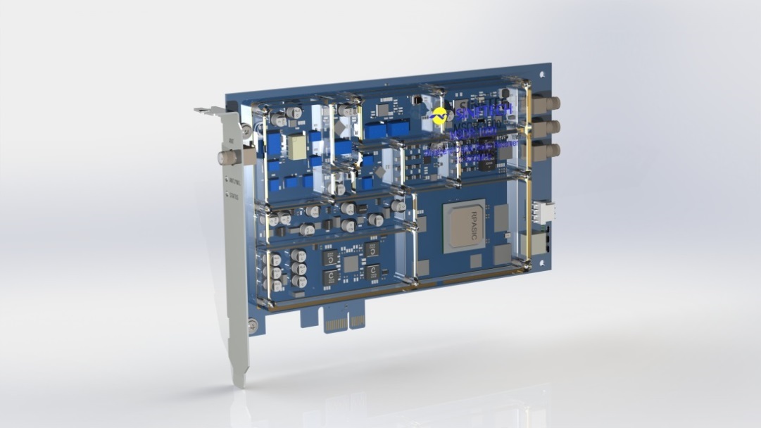
For many years I have been working in the field of creating means for capturing and processing signals from onboard and coastal navigation radars. About two years ago I released the latest, to date, version of our RVAQ (Radar Video AcQuisition) board and wondered what to do next in life. I wanted something new and unexplored. The choice fell on the area that I had not yet covered - digital radio reception with an easy entry into the microwave region.
This is the first chapter on the initial statement of the problem.
Where to start, if you never professionally engaged in digital radio, except for the receiver "Mishutka", collected in childhood? Of course, with therefreshment of the memory of Polyakov reading and the model in MATLAB. The initial idea was to create a multi-channel receiver with a range of 156-162 MHz for monitoring and recording all active conversations in the marine VHF range. I will list the desired properties of such a receiver:
1. Receive bandwidth of at least 6 MHz (162-156 = 6)
2. Sensitivity is not worse than -110dBm, or they will laugh
3. Large dynamic range, because when you listen to a ship on the shore at sea for 30 miles, someone will surely scream nearby with its 25 watts. For decent receivers, the blocking level must be at least 70 dB. Running a little ahead, I will say that it turned out to implement more than 90 dB of blocking. In short, the RTL-SDR was not at all consistent with expectations. The estimation began, oddly enough, with the choice of ADC. Since if there is no corresponding (at least in theory) ADC in nature, then it is not worth taking. Such an ADC was found.
Now you need to choose the architecture of the receiver. A review of current decisions, the study of the element base and intuition made it possible to dwell on the receiver of the direct transformation . It was also decided to transfer to the zero frequency of interest the part of the spectrum using a quadrature demodulator and work in the first Nyquist zone to maximize utilize all the qualities of the selected ADC.

')
Well, the model showed the viability of the idea - sensitivity of -115 dBm, blocking under 90 dB.

Further, in the FPGA, using the quadrature signal normalization block, we remove the DC component, deal with the mirror channel and give a signal to the DDC input. After the drift of the frequency of interest to zero, the signal will fall on the chain of digital CIC and FIR filters forming the channel strip. Of course, if we want to simultaneously receive more than one channel, we must have a bunch of DDC and filters.
In the next article, if the public is interested, I will tell you about the next steps in modeling and evaluating the hardware resources of the FPGA.
For many years I have been working in the field of creating means for capturing and processing signals from onboard and coastal navigation radars. About two years ago I released the latest, to date, version of our RVAQ (Radar Video AcQuisition) board and wondered what to do next in life. I wanted something new and unexplored. The choice fell on the area that I had not yet covered - digital radio reception with an easy entry into the microwave region.
This is the first chapter on the initial statement of the problem.
Where to start, if you never professionally engaged in digital radio, except for the receiver "Mishutka", collected in childhood? Of course, with the
1. Receive bandwidth of at least 6 MHz (162-156 = 6)
2. Sensitivity is not worse than -110dBm, or they will laugh
3. Large dynamic range, because when you listen to a ship on the shore at sea for 30 miles, someone will surely scream nearby with its 25 watts. For decent receivers, the blocking level must be at least 70 dB. Running a little ahead, I will say that it turned out to implement more than 90 dB of blocking. In short, the RTL-SDR was not at all consistent with expectations. The estimation began, oddly enough, with the choice of ADC. Since if there is no corresponding (at least in theory) ADC in nature, then it is not worth taking. Such an ADC was found.
Now you need to choose the architecture of the receiver. A review of current decisions, the study of the element base and intuition made it possible to dwell on the receiver of the direct transformation . It was also decided to transfer to the zero frequency of interest the part of the spectrum using a quadrature demodulator and work in the first Nyquist zone to maximize utilize all the qualities of the selected ADC.
Initial model for parameter estimation
clear all; k = 1.381e-23; % Joule/K - Boltzmann's Constant T0 = 290; % K - temperature % Encoding Windows-1251 % 1. % 1010 - % 1011 - % 1012 - (/.) % 1013 - % 1014 - % 1015 - % 1021, 1022 - . % 1031, 1032 - % 1041, 1042 - % 1051, 1052 - % 2. Rrf_inp_ohm = 50; % Ohm - . % 2011 - BWrf_ekv_prf_hz = 20.0e6; % Hz - Lrf_max_prf_db = 1.0; % dB - (insertion loss) % 2012 - % ( Agilent MGA-71543 ) Grf_lna_db = 16.0; % dB - NFrf_lna_db = 1.0; % dB - % 2013 - BWrf_ekv_fms_hz = 6.0e6; % Hz - Lrf_max_fms_db = 4.0; % dB - (insertion loss) % 2014 - % ( Agilent MGA-71543 ) Grf_amp_db = 16.0; % dB - NFrf_amp_db = 1.0; % dB - % 2015 - % ( Analog Devices ADL5387) Grf_mix_db = 4.5; % dB - NFrf_mix_db = 15.0; % dB - IP1dBrf_mix_dbw = 13.0 - 30.0; % dBW - Input P1dB (IP1dB) % 3. % 3011 - % (db) NFrf_sys_db = pow2db( ( db2pow( Lrf_max_prf_db ) ) + ... ( db2pow( NFrf_lna_db ) + 1 ) / ( db2pow( -Lrf_max_prf_db )) + ... ( db2pow( Lrf_max_fms_db ) + 1 ) / ( db2pow( -Lrf_max_prf_db ) * db2pow( Grf_lna_db )) + ... ( db2pow( NFrf_amp_db ) + 1 ) / ( db2pow( -Lrf_max_prf_db ) * db2pow( Grf_lna_db ) * db2pow( -Lrf_max_fms_db )) + ... ( db2pow( NFrf_mix_db ) + 1 ) / ( db2pow( -Lrf_max_prf_db ) * db2pow( Grf_lna_db ) * db2pow( -Lrf_max_fms_db ) * db2pow( Grf_amp_db )) ... ); % (dB) Grf_sys_db = ( Grf_lna_db + Grf_amp_db + Grf_mix_db ) - ( Lrf_max_prf_db + Lrf_max_fms_db ); % (Hz) BWrf_sys_hz = BWrf_ekv_fms_hz; % 3012 - Baseband LPF Lbb_lpf_db = 9; % dB - Baseband LPF (insertion loss) % 3013 - Baseband (LTC6400-14) Gbb_opa_db = 0; % dB - NFbb_opa_db = 0; % dB - % , (dB) Gbb_lfa_db = Gbb_opa_db - Lbb_lpf_db; % (dB) - . NFbb_sys_db = pow2db( ( db2pow( NFrf_sys_db ) ) + ... ( db2pow( NFbb_opa_db ) + 1 ) / ( db2pow( Grf_sys_db )) ... ); % (dB) Gbb_sys_db = Grf_sys_db + Gbb_lfa_db; % (Hz) - BWbb_sys_hz = BWrf_sys_hz; % (dBW) PNbb_out_dbw = pow2db( k * T0 * BWrf_sys_hz ) + NFbb_sys_db + Gbb_sys_db; % 3014 - % ( 1 Linear Technology LTC2271) FSadc_hz = 20.0e6; % Hz - Sampling rate SNadc_fs_db = 84; % dB - SNR NBadc_fs_bits = 16; % bits - Full scale bits Vadc_fs_v = 2; % V - Full scale voltage Radc_inp_ohm = 1000; % Ohm - Input ADC resistance % (dBW) PFSadc_inp_dbw = pow2db( 2.0 * (( Vadc_fs_v * 0.5 * sqrt( 0.5 )) ^ 2 ) / Radc_inp_ohm ); % (dBW) PNadc_snr_dbw = PFSadc_inp_dbw - SNadc_fs_db; % (dBW) PNadc_qan_dbw = PFSadc_inp_dbw - ( NBadc_fs_bits * mag2db( 2 ) + mag2db( sqrt( 6 ) / 2 )); % adding correction factor for sinusoidal signal % 3015 - SNfm_min_db = 12.0; % dB - - BWfm_max_hz = 25.0e3; % Hz - , BWfm_min_hz = 6.25e3; % Hz - , % (dBW) ( ) Pfm_min_dbw = pow2db( k * T0 * BWfm_max_hz ) + NFbb_sys_db + SNfm_min_db; % , (dBW) Pfm_min_bb_sys_dbw = Pfm_min_dbw + Gbb_sys_db; % . % (dBW) PFSmix_inp_dbw = PFSadc_inp_dbw - Gbb_lfa_db - Grf_mix_db; % ( ) deltaPmix_inp_lin = IP1dBrf_mix_dbw - PFSmix_inp_dbw; ')
Now I want pictures
% Nfft = 2 * (( FSadc_hz / 2 ) / BWfm_min_hz ); Nsmp = Nfft; tmp_fft_buf = zeros( 1, Nfft ); tmp_acc_buf = zeros( 1, Nfft ); tmp_smp_buf = zeros( 1, Nsmp ); max_acc = 30; for acc = 1:max_acc % 1 % - % - PS1 = db2pow( Pfm_min_bb_sys_dbw ); WS1 = 25.0e3; FS1 = 1.0e6; Fstart = FS1; Fstop = Fstart + WS1 - BWfm_min_hz; Pstep = PS1 / ( WS1 / BWfm_min_hz ); PS1_smp_buf = zeros( 1, Nsmp ); for f = Fstart:BWfm_min_hz:Fstop phi_acc = 2.0 * pi * rand( 1 ); % random phase phi_stp = pi * ( f / ( FSadc_hz / 2 )); for k = 1:Nsmp PS1_smp_buf( k ) = PS1_smp_buf( k ) + sqrt( Pstep ) * exp( j * phi_acc ); phi_acc = phi_acc + phi_stp; if( phi_acc > ( 2.0 * pi )) phi_acc = phi_acc - 2.0 * pi; else if( phi_acc < ( -2.0 * pi )) phi_acc = phi_acc + 2.0 * pi; end end end end % 2 % - % - PS2 = db2pow( PFSadc_inp_dbw - 1.0 ); % -1 dB back off WS2 = 25.0e3; FS2 = -2.0e6; Fstart = FS2; Fstop = Fstart + WS2 - BWfm_min_hz; Pstep = PS2; PS2_smp_buf = zeros( 1, Nsmp ); for f = Fstart:BWfm_min_hz:Fstop phi_acc = 2.0 * pi * rand( 1 ); % random phase phi_stp = pi * ( f / ( FSadc_hz / 2 )); for k = 1:Nsmp PS2_smp_buf( k ) = PS2_smp_buf( k ) + sqrt( Pstep ) * exp( j * phi_acc ); phi_acc = phi_acc + phi_stp; if( phi_acc > ( 2.0 * pi )) phi_acc = phi_acc - 2.0 * pi; else if( phi_acc < ( -2.0 * pi )) phi_acc = phi_acc + 2.0 * pi; end end end end % PN1 = db2pow( PNbb_out_dbw ); WN1 = BWbb_sys_hz; Pfull_bw = PN1 * ( FSadc_hz / WN1 ); PN1_smp_buf = sqrt( 0.5 * Pfull_bw ) * complex( randn( 1, Nsmp ), randn( 1, Nsmp )); tmp_fft_buf = fftshift( fft( PN1_smp_buf )); tmp_msk_buf = zeros( 1, Nfft ); tmp_msk_buf((( Nfft / 2 ) - (( WN1 / FSadc_hz ) * ( Nfft / 2 )) + 1 ) : (( Nfft / 2 ) + (( WN1 / FSadc_hz ) * ( Nfft / 2 )))) = ... ones( 1, (( WN1 / FSadc_hz ) * Nfft )); tmp_fft_buf = tmp_fft_buf .* tmp_msk_buf; PN1_smp_buf = ifft( fftshift( tmp_fft_buf )); % PN2 = db2pow( PNadc_snr_dbw ) - db2pow( PNadc_qan_dbw ); %PN2 = db2pow( PNadc_snr_dbw ); Pfull_bw = PN2; PN2_smp_buf = sqrt( 0.5 * Pfull_bw ) * complex( randn( 1, Nsmp ), randn( 1, Nsmp )); % QAN_smp_buf = PS1_smp_buf + PS2_smp_buf + PN1_smp_buf + PN2_smp_buf; QAN_delta = Vadc_fs_v / ( 2 ^ NBadc_fs_bits ); QAN_smp_buf = round( QAN_smp_buf ./ QAN_delta ) .* QAN_delta; QAN_smp_buf_re = real( QAN_smp_buf ); QAN_smp_buf_re( find( QAN_smp_buf_re > ( Vadc_fs_v / 2.0 ))) = Vadc_fs_v / 2.0; QAN_smp_buf_re( find( QAN_smp_buf_re < ( -Vadc_fs_v / 2.0 ))) = -Vadc_fs_v / 2.0; QAN_smp_buf_im = imag( QAN_smp_buf ); QAN_smp_buf_im( find( QAN_smp_buf_im > ( Vadc_fs_v / 2.0 ))) = Vadc_fs_v / 2.0; QAN_smp_buf_im( find( QAN_smp_buf_im < ( -Vadc_fs_v / 2.0 ))) = -Vadc_fs_v / 2.0; QAN_smp_buf = complex( QAN_smp_buf_re, QAN_smp_buf_im ); % ADC tmp_smp_buf = QAN_smp_buf; %tmp_smp_buf = PS1_smp_buf + PS2_smp_buf + PN1_smp_buf + PN2_smp_buf; tmp_fft_buf = fft( tmp_smp_buf ) / Nfft; tmp_acc_buf = tmp_acc_buf + ( tmp_fft_buf .* conj( tmp_fft_buf )); end tmp_acc_buf = tmp_acc_buf ./ max_acc; f = linspace(( -FSadc_hz / 2 ) + BWfm_min_hz, FSadc_hz / 2, Nfft ); plot( f, pow2db( fftshift( tmp_acc_buf ))); xlim( [( -FSadc_hz / 2 ), ( FSadc_hz / 2 )] ); ylim( [-150.0, -20.0] ); title('Power Spectrum') xlabel('Frequency (Hz)') ylabel('P(f) dBW') drawnow; Well, the model showed the viability of the idea - sensitivity of -115 dBm, blocking under 90 dB.
Further, in the FPGA, using the quadrature signal normalization block, we remove the DC component, deal with the mirror channel and give a signal to the DDC input. After the drift of the frequency of interest to zero, the signal will fall on the chain of digital CIC and FIR filters forming the channel strip. Of course, if we want to simultaneously receive more than one channel, we must have a bunch of DDC and filters.
In the next article, if the public is interested, I will tell you about the next steps in modeling and evaluating the hardware resources of the FPGA.
Source: https://habr.com/ru/post/395853/
All Articles