Inside IBM FlashSystem 900
The IBM FlashSystem family is the result of many years of development and investment of $ 1 billion in flash technology. The internal structure of AFAs is often the strictest trade secret. Manufacturers, as a rule, focus on marketing (how quickly data will be processed, write / read speed, reliability), but do not disclose the details of the structure of the systems.
Not so long ago, IBM provided an opportunity to view the components of its FlashSystem 900, which works as a stand-alone device and provides 1 million / 600,000 IOPS with random read / write and 10.5 / 4.5 Gb / s I / O with sequential read / write. FlashSystem 900 also serve as a component in more large systems from the same IBM, FlashSystem V9000 and A9000 AFAs. Therefore, familiarizing yourself with FlashSystem 900 allows you to see the difference between a component and a larger system created from these components.
')
Flash masses evolved over several years, but they began with the use of conventional SSD drives of the standard 2.5-inch form factor, which were connected to storage systems designed for HDD drives. Using SSD allowed to significantly speed up the system compared to HDD. But this did not solve the problem to the full, the bottlenecks simply wandered into other components of the array (RAID controller or network interface).
Pioneers of flash arrays began to develop optimized SSD devices with faster internal components and optimized data transfer channels, while the needs of data processing centers were only growing. Most AFA manufacturers still use 2.5 SSDs. The latest AFAs based on 2.5 SSDs provide users with high performance and fault tolerance, but the capabilities of such SSDs are limited due to factory firmware.
Other vendors such as IBM, XtremIO (EMC) and Violin created their own AFAs using specially designed flash modules. These new products provide the ability to control NAND itself, which, in turn, makes it possible to control data storage density, performance, durability and cost effectiveness.
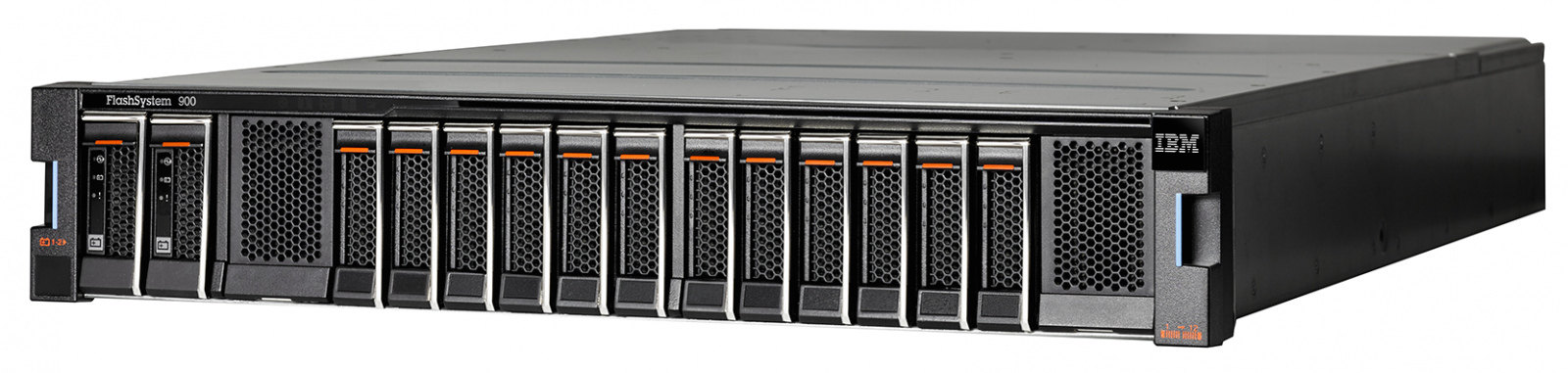
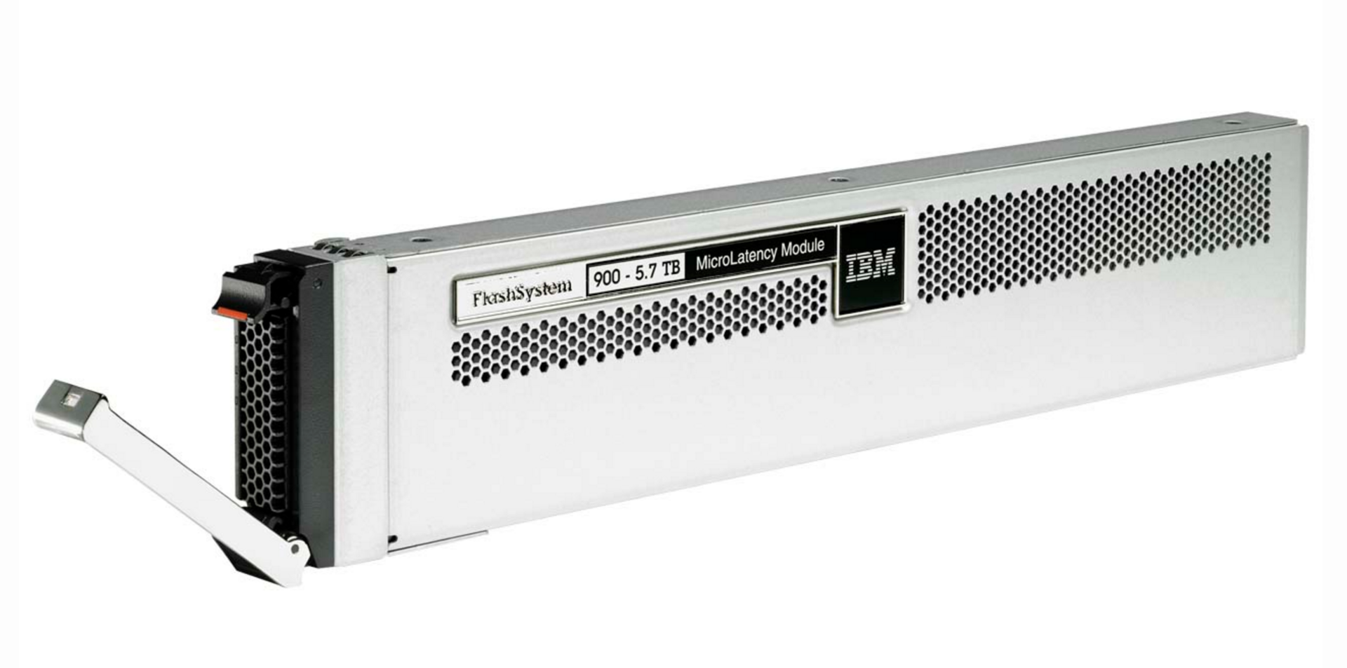
FlashSystem 900 is a 2U chassis that holds 12 hot-pluggable MicroLatency modules, as shown in the image below. In addition, the system has two large lithium-ion batteries (left), which provide enough power to complete the recording process in cases of failure of the main power source. Batteries provide enough power to shut down the array correctly and without any data loss.

Each MicroLatency module can contain 1.2 TB, 2.9 TB or 5.7 TB of flash memory. In turn, the system records data through a single module. The modules themselves are configured in RAID 5 to ensure maximum data integrity when one of the modules fails. IBM also uses its own flash variable RAID path at the flash memory level to create a two-dimensional parity control scheme.
Each MicroLatency module has a dual PCB design with Xilinx Kintex-7 PVM. Each PCB can hold up to four FPGAs, but the number of FPGAs varies depending on the density of the module. For example, a 1.2 TB module will use only one FPGA on a single PCB. Using an architecture with multiple FPGAs allows IBM to scale performance and power linearly.
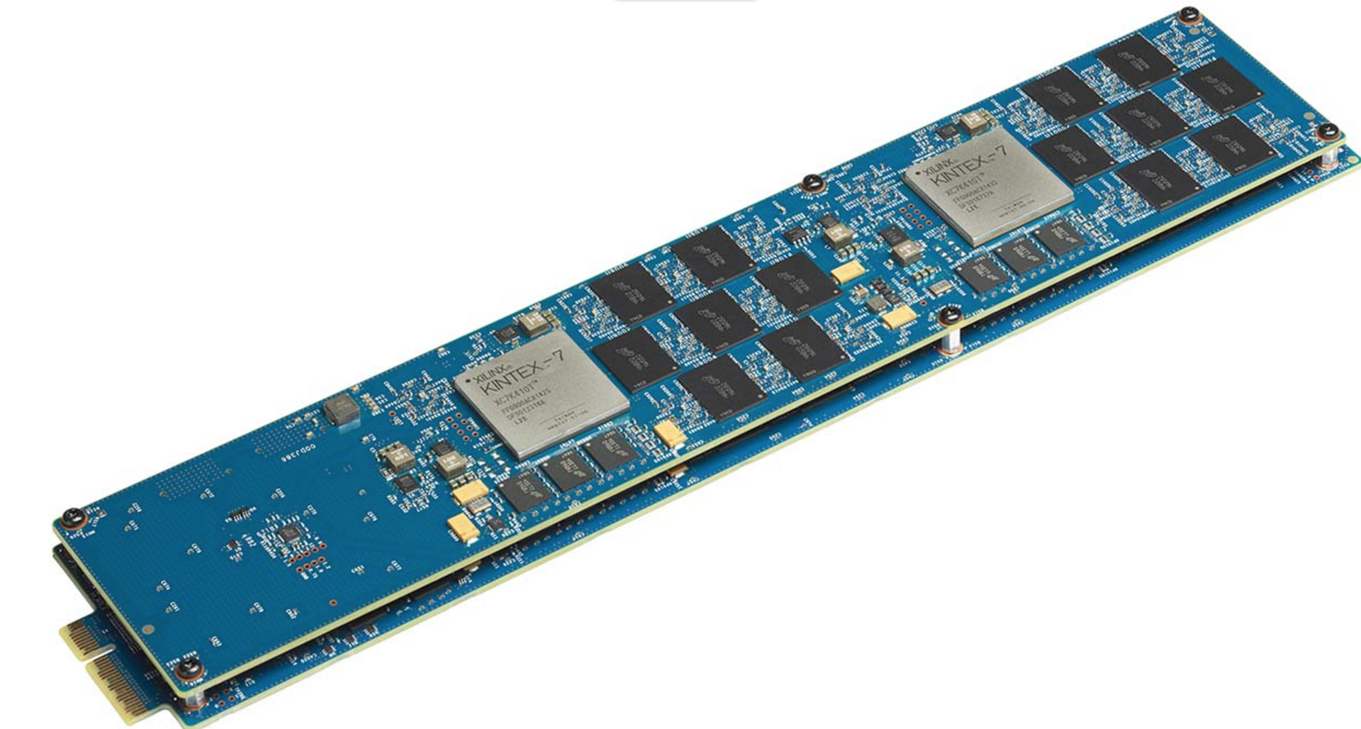
A closer look at the back of the board shows two PCIe 3.0 x2 connections on the left side. These slots are used to connect to the host and communicate using a serial protocol patented by IBM. The protocol provides similar advantages to NVM Express: reduced processor load, latency, and increased performance. The proprietary protocol uses hardware-accelerated data transfer channel with pass-through routing to eliminate the processes causing delays, such as interrupts.

Each FPGA has its own DRAM for managing LBAs, and IBM also uses DRAM for caching user data.
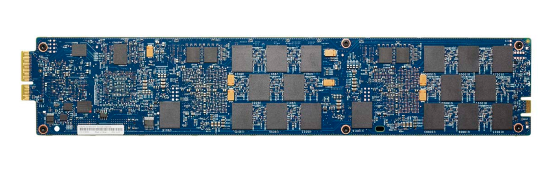
Most SSDs do not cache user data in DRAM, but the approach to protecting power loss at the system level (through batteries) provides IBM with several advantages. Separate SSDs used in FlashSystem 900 do not require special capacitors that use ordinary 2.5-inch SSD drives. This allows the company to pack more flash memory into a project. A smaller number of capacitors also reduces the number of potential points of failure and the complexity of the software.
Several capacitors are still located between the flash memory packs, but they are used to combat voltage drops when the system simultaneously writes to several NAND packets.
IBM has established a strategic partnership with Micron to use FortisFlash NAND, which is customizable and provides additional programming capabilities in the system. This allows IBM to dynamically change the core programming of each unit over the course of a NAND life based on age and health. Micron indicated that when properly configured, the MLC FortisFlash NAND can offer up to 10,000 rewriting cycles (more than three times the standard estimate of 3,000 cycles).
There are many different types of ECC, such as BCH and LDPC, and each has its own advantages and disadvantages. AFA vendors that use a 2.5-inch SSD are limited to ECC, they can only use the manufacturer-installed SSD drive. But custom design provides the flexibility to use custom ECC algorithms.
IBM developed its own ECC algorithm. This implementation oscillates between the BCH, which is an intensive method, but has limited error correction capabilities, and LDPC, which can be subject to excessive recording gain during the error correction process (thus reducing wear resistance). IBM believes that custom “read once” error correction includes the best of both methods.
IBM also uses heat segregation, which detects hot and cold data and then combines them to reduce wear. The company dynamically tracks the remaining number of possible overwrites of each cell, so rarely changing “cold” data is stored in older NAND cells. Due to what remains wear resistance. IBM claims that thermal insulation increases endurance by 49 percent, and the addition of selective wear leveling (based on NAND health) increases endurance by 57 percent.
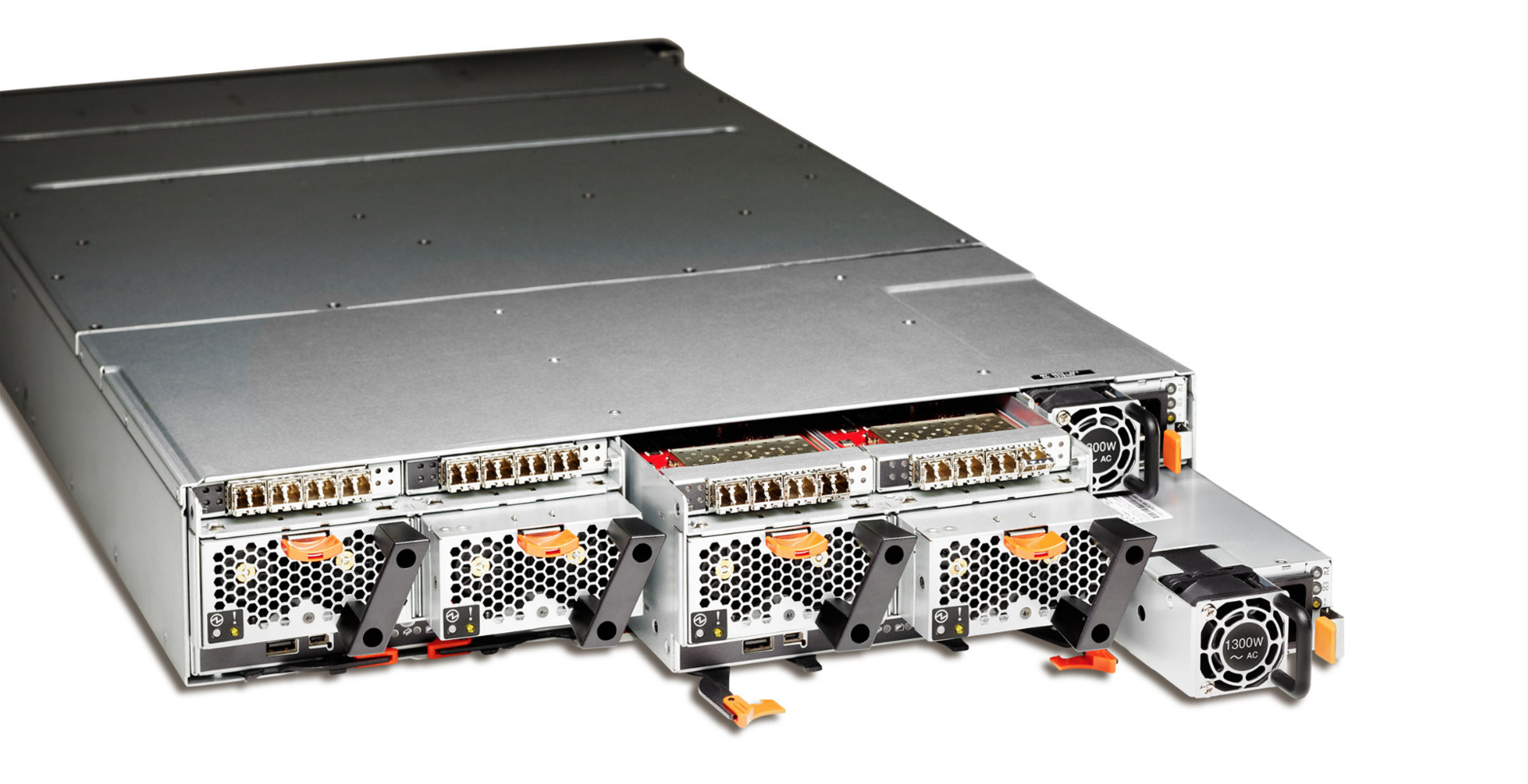
Each 2U chassis contains two redundant power supplies right behind the front panel of an affordable, hot-swappable battery. The system has four hot-swappable, modular fans placed in two large block canisters (left). Each of these has a number of I / O ports (Fiber Channel, iSCSI and FCoE range) along the top, which are located on the hot-swappable interface cards.
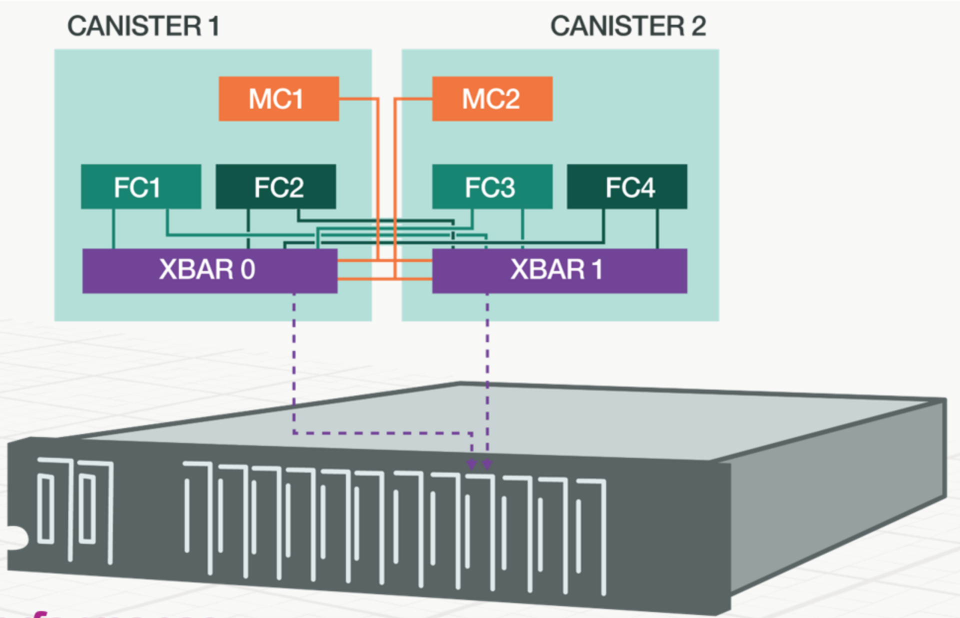
Each canister contains two processors from the Intel Xeon E5v2 series, 64GB of RAM, and a RAID controller (XBAR). The canisters are also hot-swappable in order to minimize downtime in the event of a failure in the computed part of the system or memory. The design itself is optimized to provide a maximum of two hops and never more from data input / output ports to flash memory, which guarantees stable performance and steel latency.
IBM acquired Texas Memory Systems in 2012 and made additional investments of $ 1 billion in flash technology development in 2013. This allowed the company to develop customized flash arrays that have higher performance and reliability than typical flash arrays using 2.5 SSDs. IBM claims that the FlashSystem family provides 9.41 percent more endurance than competing solutions and provides it with a seven-year warranty. IBM specialists can increase the memory density in their MicroLatency modules, providing protection against power losses throughout the system. They can do this using their own hardware-controlled, serial interface that eliminates software-induced delays. The company developed its own architecture to provide a number of advantages, such as user ECC and adaptive NAND algorithms, which provide great benefits to the end user in terms of density, performance and cost.
IBM is not the only company in the flash array race. EMC recently introduced an entire line of flash devices, some of which used non-standard SSD designs. The company completely transfers all its data storage systems to the use of flash memory. Pure Storage also has a promising initiative with the FlashBlade device, but this platform is still not available on the market at the moment. Violin Memory also has an individual project, but its poor performance and dark prospects discourage many from using this solution.
IBM among the main suppliers of AFA in terms of performance, but not the first in revenue. The company claims that in the end result of an individual project, they will offer higher performance flash memory at a lower cost than competitors.
It is clear that the future, based on flash memory technology, will bring even more specialized and optimized projects. Probably - this will lead to the death of many systems (and companies) that use 2.5 inch SSD market drives.
Not so long ago, IBM provided an opportunity to view the components of its FlashSystem 900, which works as a stand-alone device and provides 1 million / 600,000 IOPS with random read / write and 10.5 / 4.5 Gb / s I / O with sequential read / write. FlashSystem 900 also serve as a component in more large systems from the same IBM, FlashSystem V9000 and A9000 AFAs. Therefore, familiarizing yourself with FlashSystem 900 allows you to see the difference between a component and a larger system created from these components.
')
Flash Array Evolution
Flash masses evolved over several years, but they began with the use of conventional SSD drives of the standard 2.5-inch form factor, which were connected to storage systems designed for HDD drives. Using SSD allowed to significantly speed up the system compared to HDD. But this did not solve the problem to the full, the bottlenecks simply wandered into other components of the array (RAID controller or network interface).
Pioneers of flash arrays began to develop optimized SSD devices with faster internal components and optimized data transfer channels, while the needs of data processing centers were only growing. Most AFA manufacturers still use 2.5 SSDs. The latest AFAs based on 2.5 SSDs provide users with high performance and fault tolerance, but the capabilities of such SSDs are limited due to factory firmware.
Other vendors such as IBM, XtremIO (EMC) and Violin created their own AFAs using specially designed flash modules. These new products provide the ability to control NAND itself, which, in turn, makes it possible to control data storage density, performance, durability and cost effectiveness.
IBM FlashSystem 900
FlashSystem 900 is a 2U chassis that holds 12 hot-pluggable MicroLatency modules, as shown in the image below. In addition, the system has two large lithium-ion batteries (left), which provide enough power to complete the recording process in cases of failure of the main power source. Batteries provide enough power to shut down the array correctly and without any data loss.
Each MicroLatency module can contain 1.2 TB, 2.9 TB or 5.7 TB of flash memory. In turn, the system records data through a single module. The modules themselves are configured in RAID 5 to ensure maximum data integrity when one of the modules fails. IBM also uses its own flash variable RAID path at the flash memory level to create a two-dimensional parity control scheme.
Each MicroLatency module has a dual PCB design with Xilinx Kintex-7 PVM. Each PCB can hold up to four FPGAs, but the number of FPGAs varies depending on the density of the module. For example, a 1.2 TB module will use only one FPGA on a single PCB. Using an architecture with multiple FPGAs allows IBM to scale performance and power linearly.
A closer look at the back of the board shows two PCIe 3.0 x2 connections on the left side. These slots are used to connect to the host and communicate using a serial protocol patented by IBM. The protocol provides similar advantages to NVM Express: reduced processor load, latency, and increased performance. The proprietary protocol uses hardware-accelerated data transfer channel with pass-through routing to eliminate the processes causing delays, such as interrupts.
Each FPGA has its own DRAM for managing LBAs, and IBM also uses DRAM for caching user data.
Most SSDs do not cache user data in DRAM, but the approach to protecting power loss at the system level (through batteries) provides IBM with several advantages. Separate SSDs used in FlashSystem 900 do not require special capacitors that use ordinary 2.5-inch SSD drives. This allows the company to pack more flash memory into a project. A smaller number of capacitors also reduces the number of potential points of failure and the complexity of the software.
Several capacitors are still located between the flash memory packs, but they are used to combat voltage drops when the system simultaneously writes to several NAND packets.
IBM has established a strategic partnership with Micron to use FortisFlash NAND, which is customizable and provides additional programming capabilities in the system. This allows IBM to dynamically change the core programming of each unit over the course of a NAND life based on age and health. Micron indicated that when properly configured, the MLC FortisFlash NAND can offer up to 10,000 rewriting cycles (more than three times the standard estimate of 3,000 cycles).
There are many different types of ECC, such as BCH and LDPC, and each has its own advantages and disadvantages. AFA vendors that use a 2.5-inch SSD are limited to ECC, they can only use the manufacturer-installed SSD drive. But custom design provides the flexibility to use custom ECC algorithms.
IBM developed its own ECC algorithm. This implementation oscillates between the BCH, which is an intensive method, but has limited error correction capabilities, and LDPC, which can be subject to excessive recording gain during the error correction process (thus reducing wear resistance). IBM believes that custom “read once” error correction includes the best of both methods.
IBM also uses heat segregation, which detects hot and cold data and then combines them to reduce wear. The company dynamically tracks the remaining number of possible overwrites of each cell, so rarely changing “cold” data is stored in older NAND cells. Due to what remains wear resistance. IBM claims that thermal insulation increases endurance by 49 percent, and the addition of selective wear leveling (based on NAND health) increases endurance by 57 percent.
Each 2U chassis contains two redundant power supplies right behind the front panel of an affordable, hot-swappable battery. The system has four hot-swappable, modular fans placed in two large block canisters (left). Each of these has a number of I / O ports (Fiber Channel, iSCSI and FCoE range) along the top, which are located on the hot-swappable interface cards.
Each canister contains two processors from the Intel Xeon E5v2 series, 64GB of RAM, and a RAID controller (XBAR). The canisters are also hot-swappable in order to minimize downtime in the event of a failure in the computed part of the system or memory. The design itself is optimized to provide a maximum of two hops and never more from data input / output ports to flash memory, which guarantees stable performance and steel latency.
Wider Relevance.
IBM acquired Texas Memory Systems in 2012 and made additional investments of $ 1 billion in flash technology development in 2013. This allowed the company to develop customized flash arrays that have higher performance and reliability than typical flash arrays using 2.5 SSDs. IBM claims that the FlashSystem family provides 9.41 percent more endurance than competing solutions and provides it with a seven-year warranty. IBM specialists can increase the memory density in their MicroLatency modules, providing protection against power losses throughout the system. They can do this using their own hardware-controlled, serial interface that eliminates software-induced delays. The company developed its own architecture to provide a number of advantages, such as user ECC and adaptive NAND algorithms, which provide great benefits to the end user in terms of density, performance and cost.
IBM is not the only company in the flash array race. EMC recently introduced an entire line of flash devices, some of which used non-standard SSD designs. The company completely transfers all its data storage systems to the use of flash memory. Pure Storage also has a promising initiative with the FlashBlade device, but this platform is still not available on the market at the moment. Violin Memory also has an individual project, but its poor performance and dark prospects discourage many from using this solution.
IBM among the main suppliers of AFA in terms of performance, but not the first in revenue. The company claims that in the end result of an individual project, they will offer higher performance flash memory at a lower cost than competitors.
It is clear that the future, based on flash memory technology, will bring even more specialized and optimized projects. Probably - this will lead to the death of many systems (and companies) that use 2.5 inch SSD market drives.
Source: https://habr.com/ru/post/395715/
All Articles