Shadowplay LED Watch on the Arduino Uno Platform
Instead of intro
So, our team of three people was faced with the task: to assemble a small hardware project in a very short time, preferably on the Arduino platform. It is worth making a reservation that up to that moment we were familiar with circuitry, for the most part, in theory. And that means - neither the experience with a soldering iron (practically), nor, all the more, the experience with an Arduino.
Suddenly, we stumbled upon an article dedicated to the project Shadowplay Clock. This wall clock, designed by a team of Viennese designers, the time on which you can see by touching your finger to their center. The LEDs light up in such a way that the finger shadow in the center shows the time. It was decided to create the same (or very similar), but at home. The above article, as you can see, does not contain a detailed description of the project. From all this it followed that we ourselves had to figure out how this device worked, and bring it to life. What we actually do.
Materials
To create watches you need:
')
- fiberboard blanks
- 60 diode LED strip
- Arduino uno
- RTC DS1307 real time clock module
- button
- bread board
- shift register 74HC595 (x2)
- 8-bit register latch 74HC573N (x8)
- 4-16 K155ID3 decoder
- open drain inverter IN74HC05AN (x10)
- Power Supply
Let's get started
So, the algorithm of the device:
- When power is applied, the LEDs turn on in the specified combination. In the original Shadowplay, all the LEDs light up, but it seemed to us that it would be more interesting to launch some combination as a screensaver.
- When you press the button (yes, we also moved away from the original and inserted a small button in the center), the time is read from the RTC module.
- The read time is converted into a binary code (mask) and entered into registers.
- Depending on the mask, the required diode is lit.
Hardware
When we finally decided on the idea of the project, first of all we tried to mentally sketch out approximate versions of schemes for its implementation. The main question was how to address 60 LEDs. As a matter of fact, the answer to this question determined the way of constructing practically the whole scheme.
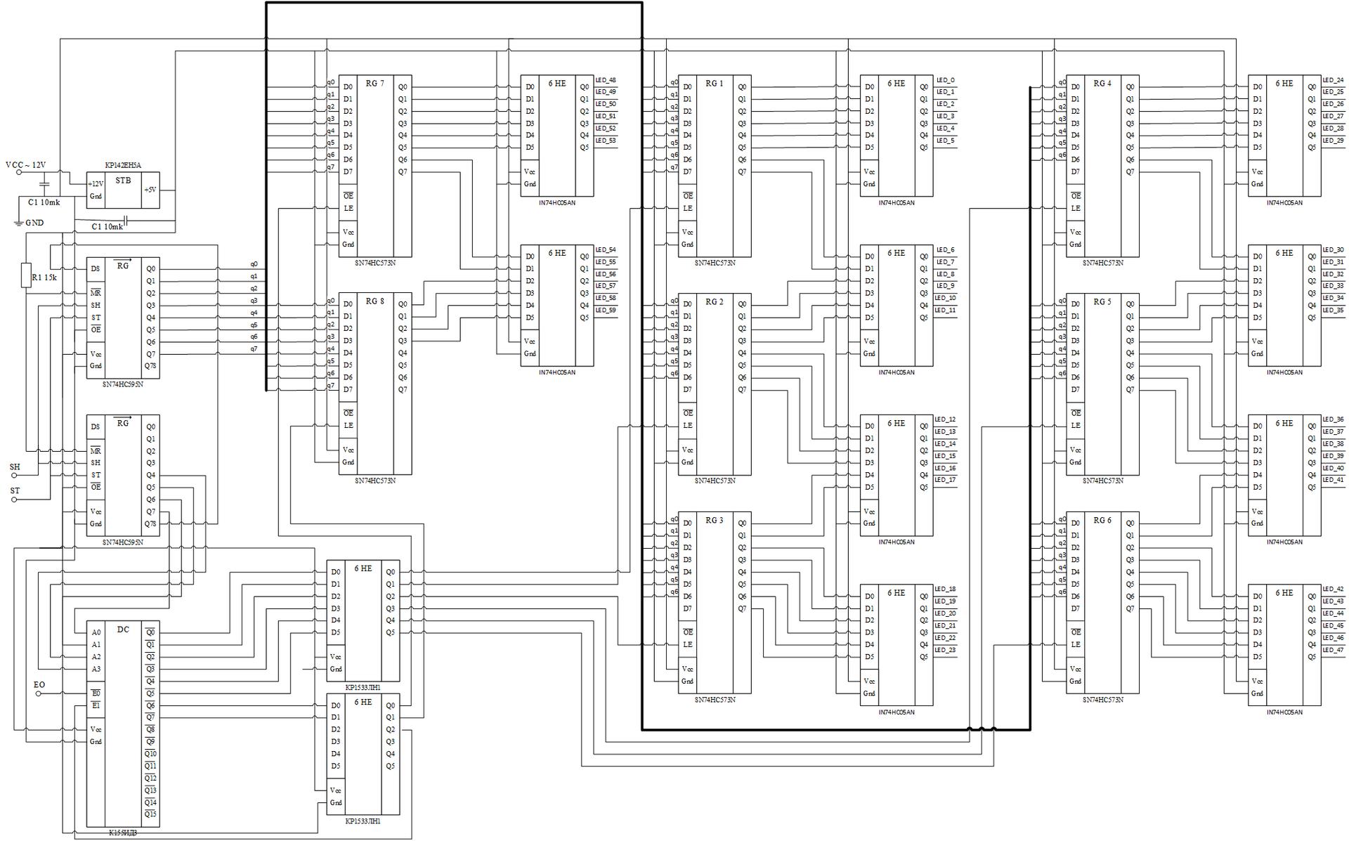
The first option that came to mind was associated with the use of decoders. The scheme was a cascade of four decoders 4 - 16 and one decoder 2 - 4, both of which with decoding enable inputs. Such a cascade made it possible to provide addressing to 64 outputs, which was enough to connect 60 LEDs.
However, then the question arose about how with this scheme at the same time get to work (address) more than one LED (after all, we needed to provide the clock with at least the minute and hour hands). This is where the main drawback of this scheme manifested itself - the decoder cannot, by definition, address more than one output simultaneously.
This flaw forced us to abandon the idea of a cascade of decoders. In addition, now we have another requirement for the future scheme - support for the simultaneous operation of a different number of LEDs.
To satisfy this requirement, we thought that it would be possible to allow each LED to store its state. Registers are well suited for this purpose, where each individual digit corresponds to the state of one of the LEDs. We decided to use registers for 8 bits, as they are more common and more practical. Accordingly, in our scheme, we need 8 such registers to provide support for 60 LEDs.
Then we thought about how to manage the state of LEDs with Arduino through registers. Each register for normal operation must receive all 8 bits entirely. Arduino Uno, of course, provides enough outputs for transmitting several bits at the same time, but this approach would not be rational. In addition, there are only 8 registers in the scheme, which means you need to address them somehow. For this purpose, we added a descrambler and two 8-bit shift registers connected by a cascade to the circuit. One shift register stores an 8-bit state mask that will be loaded into one of 8 regular registers, the number of which is stored in the second shift register. Accordingly, a descrambler is connected to the second shift register. For these purposes, a decoder is enough for 3 to 8.
To remove the inversion from the required number of outputs, we used two inverter circuits KR1533LN1. This, of course, somewhat complicated the scheme.
Another task was the operating voltage of the LEDs equal to 12 volts compared with 5 volts of logic chips. The proposed solution was to use an open drain inverter. Such a microcircuit plays the role of a key that closes (with logical 1) or opens (with logical 0) one of the contacts of the LED with the ground, thereby turning on or off the LED. The circuit assumes work from 12 volts, in accordance with the operating voltage of the LEDs, therefore, in order to get 5 volts for logic chips, a stabilizer KR142EN5A with two capacitors was added to the circuit.
Some inputs of certain microcircuits imply a constant value at the input, so they were brought to the ground or power supply. In this case, these are the following inputs:
- Inverse reset MR input in both shift registers through the load register is connected to the output of the stabilizer at 5 volts.
- The inverse enable input output OE in both shift registers is connected directly to ground.
- The inverted enable input of the E0 decoder is connected to ground
The circuit is controlled by four inputs (E1, SH, ST, DS). The purpose and signal levels of each of them will be discussed in more detail below:
Input E1 is designed to enable the decoder. In our case, initially there are two control inputs E1, E0 on the decoder, and both of them are inverse. Output will be enough and one, so the second (E0) can be brought to the ground. The state of the decoder “by default” is operational until you have a high signal level at E1. In order to do the opposite, we connected this input to the inverter. Without this, the decoder may issue incorrect control signals to the registers, for example, at the time of updating the data in the shift register. As already mentioned, a 3 by 8 decoder can be used in the circuit, which can have one non-inverse control input, which will make it possible to easily solve all the problems described above without unnecessary wires and a soldering iron.
When applying a single signal level to E1, the decoder decodes the address of the register located in the corresponding shift register, and sends a signal to the desired output. After that, the decoder is turned off again by applying a low level signal to E1. Such a switching of the decoder generates a signal at the desired output, the front and the fall of which serve to register the clock pulse for snapping into itself the data stored on the bus.
The following three inputs are intended to control shift registers. It is worth starting with the simplest thing - DS data entry. This input, as the name implies, is intended for data transmission. Since the shift registers in the circuit are connected in cascade, DS is the corresponding output of one of them. The input of the second shift register is connected to the output of the last digit of the first register. The result is a single shift register for 16 bits, of which only 12 bits are used.
The SH input is the clock input. This input is supplied with a meander, which is responsible for loading and shifting data in each of the registers, respectively, this contact of the circuit is connected to the SHCP pins of both registers.
The last pin of the ST is the data latch on the register outputs. A pulse is fed to this input, but it is fed only when the data in the shift register are loaded finally and it is required to fix them at the output of the registers. Only after the application of this signal, the loaded data inside the register on the first row of triggers fall on the second row of triggers and become available on the bus. ST is a contact connected to the STcp pins of both registers.
It remains to explain the layout of the two outputs of the MR and OE shift registers. The first input (MR) is responsible for resetting data within the register. In this scheme, this possibility is not required, therefore, a high signal level is applied to this output through the load.
The second register input (OE) is responsible for disabling the second row of triggers inside the shift register from the bus, i.e., the enable input. This function is also not required, so the output starts on the ground.
Another contact not described above is designed to remove the level of the signal from the button in the center of the clock, the button's pattern is typical and represents the load and key, depending on the position of which a low or high signal is applied to the Arduino. Depending on the button state, the clock works either in the screen saver mode or in the time display mode.
Connecting to an Arduino has no features, except that the SH pin ideally connects to the SCK digital pin. The remaining outputs of the circuit can be connected to any of the available general-purpose digital inputs. In our case, the connection is as follows:
- Arduino pin13 (SCK) - SH circuit output
- Arduino pin 11 - output circuit ST Arduino pin 8 - output circuit DS Arduino pin 5 - output circuit E1 Arduino pin 3 - output button Arduino pin GND - circuit ground (also connects to the power supply ground)
After the design was completed, work began on the basis for the clock.
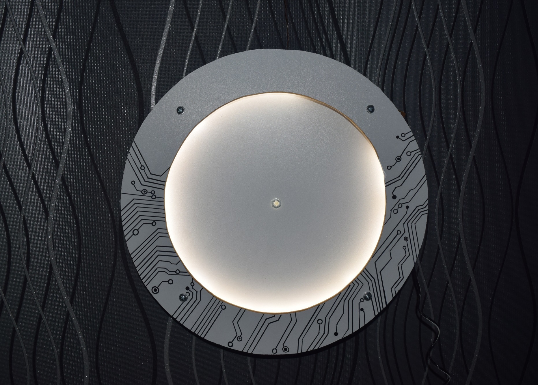
The blanks were made of fiberboard: a circle with a diameter of 36 cm - the back of the clock; and a ring measuring 36 cm (outer diameter) \ 26 cm (inner diameter) - the front part. In the original, Shadowplay has a circle diameter of 72 cm, but 36 was enough for us. The LED tape, previously cut into 60 pieces (diode + resistor), is glued to the circle. On the border of the circle drilled holes. Through them, the wires connected to the LEDs will be connected to the breadboard, which is located on the back of the circle.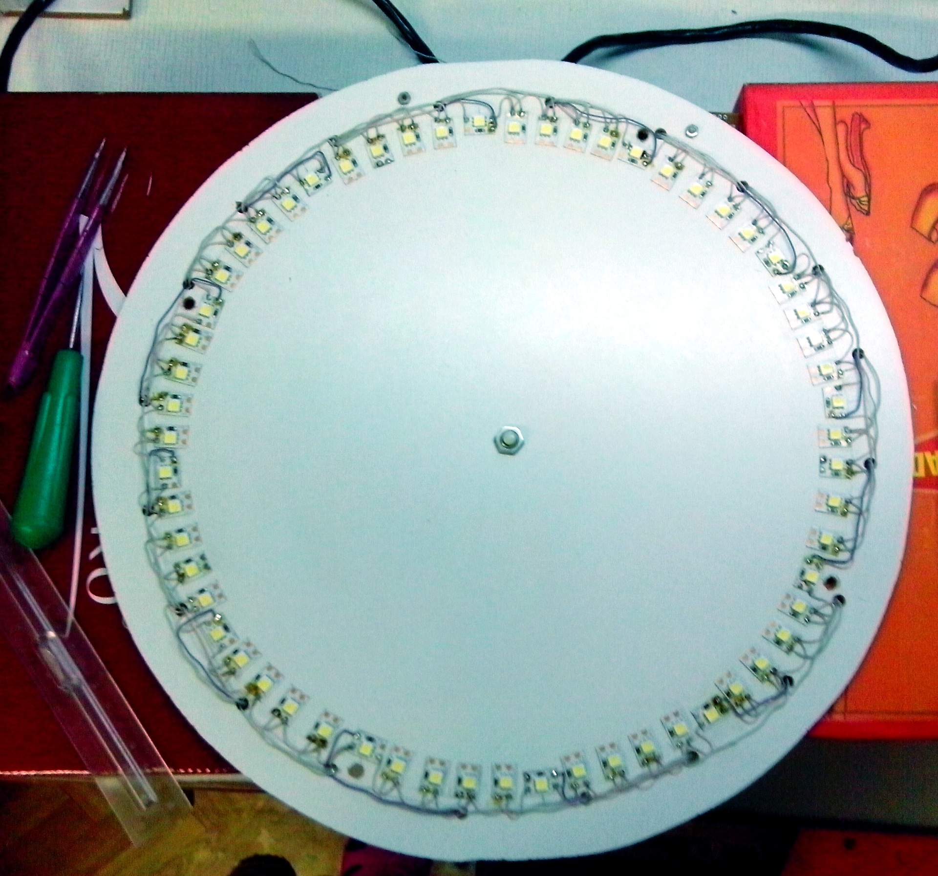
In fact, the LEDs brought a lot of headaches. Simply sticking them to the surface of the circle, we did not slightly calculate. The result was that the shadow LEDs were not bright enough. And therefore it was necessary to spend a lot of time to “lift” their degrees by 50 - 60, placing triangular cardboard linings under each of them. Yes, 60 small cardboard triangles. Therefore note: do not repeat our bitter experience - stock up on pads in advance.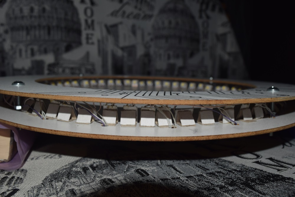
We were running out of time, and there was no time to erase the PCB. Therefore, a volitional decision was made - to assemble the project on a breadboard. The fact that such a scheme is not easy enough to assemble on a breadboard, we found out much later. Well, negative experience is also an experience.Development board and general view of the device from behind.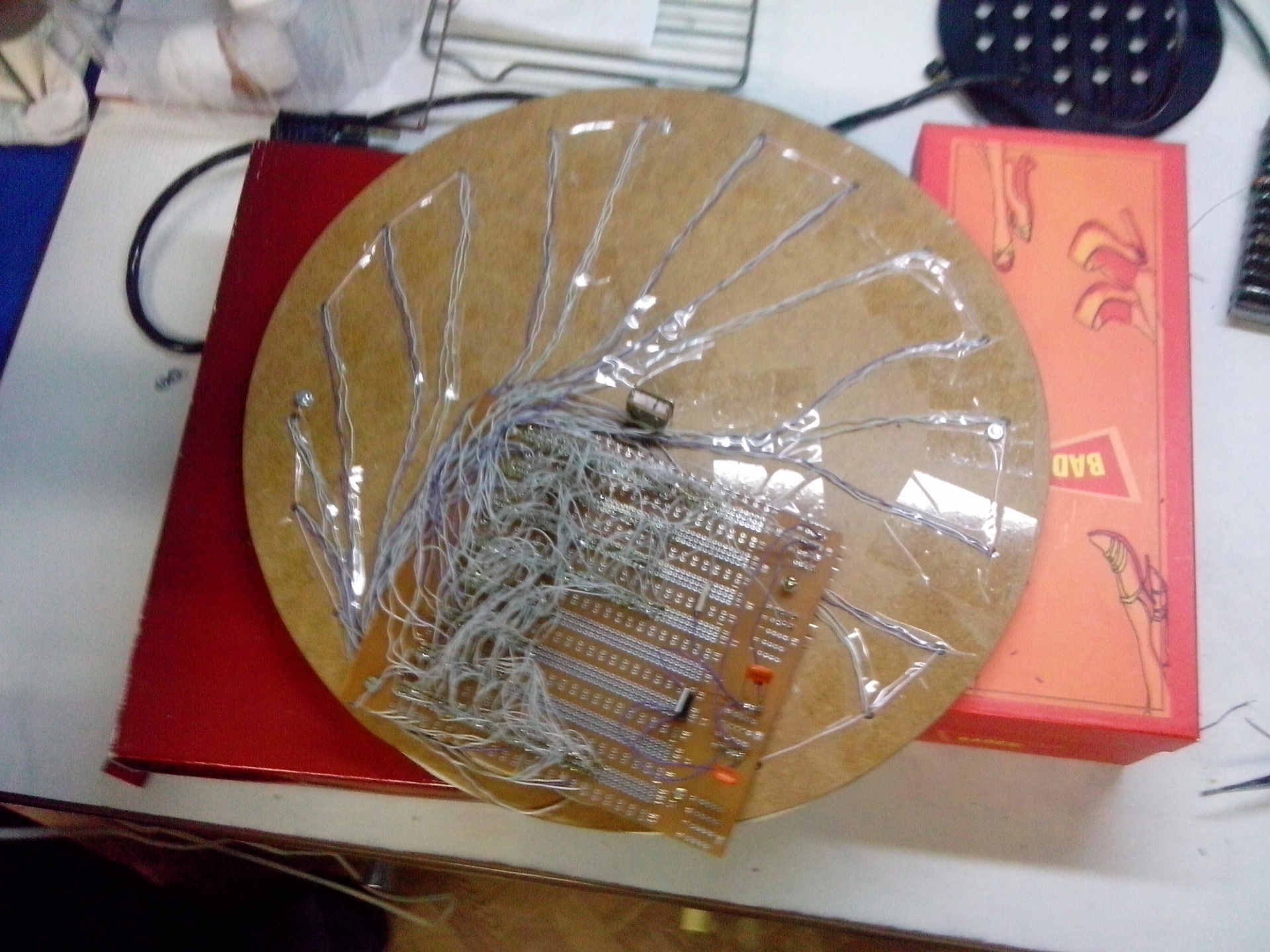
Yes, yes, we are ashamed.
It was originally planned to make an exact copy of Shadowplay. However, the way in which the user's finger is detected in the center of the device was not described in the article. After reflection, we came to the conclusion that a photoresistor is possible for these purposes. However, they soon abandoned this idea, since the photoresistor may have a random response. The device can be in conditions of varying degrees of illumination, which means it will not always be able to detect a finger with 100% probability. The preference was given to the button, which we placed in the center of the structure. It has one more advantage besides reliability. Despite its small size, the shadow of it is perfect for the role of a clock hand. Thus, if desired, the device can be programmed to work continuously in the clock mode and without putting a finger.
After the whole circuit was soldered (long sleepless nights of painstaking work with a soldering iron and tweezers), the inverters' leads are connected to the LEDs, a solemn moment has come - the first attempt to turn on the device. And, lo and behold, the diodes really burned! But not all. At first, it appeared that something was nevertheless wrongly welded. However, as it turned out, the reason was different. Since at the first start we connected not all the control inputs of logic chips, but only the most necessary ones, an ambiguity in the voltage levels appeared on the remaining unplugged inputs. In addition, the circuit was assembled on a mock-up board, with a large pile of wires, and not etched. The wires were significantly affected by electromagnetic radiation. Consequently, at the slightest voltage jump due to pickup on non-connected inputs, the logic element could work. As a result, any object in close proximity to the board caused EMP and, accordingly, unpredictable behavior of logic, and with it the LEDs.
As a result, the problem had a fairly simple solution. It was enough to initialize the inputs of all the logic elements on the circuit. Those. fully connect the circuit so that there are no unused inputs, (inputs, outputs do not affect this problem, because the logic of the chips does not depend on them), and everything fell into place.Software part
So, the hardware is finished (practically). It was the turn of writing a program for Arduino. First of all, it is necessary to configure the RTC module, namely, add time to it. The chip is based on a high-precision DS1307 module, the connection interface is I2C. The internal calendar in it is calculated to 2100, taking into account leap years. Due to the battery charge, the module can operate autonomously for about one year. Below is a diagram of the connection of RTC to Arduino, found on this site . It also took a lot of information about the RTC module.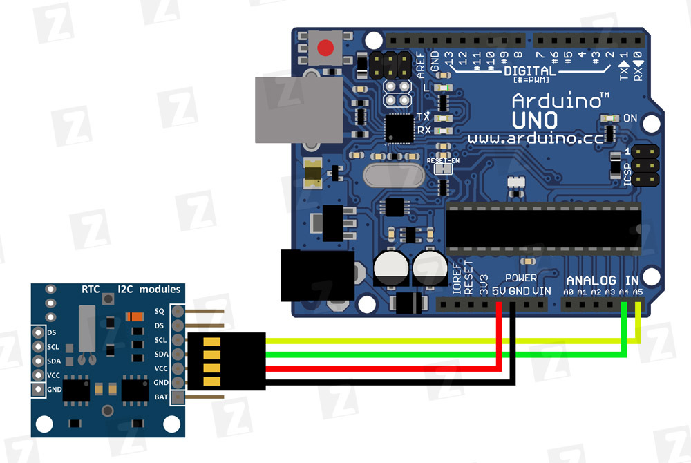
After that, it remained only to write a code that reads the time from the RTC, converts it into a mask and sends it to the board.Code#include <Time.h> #include <DS1307RTC.h> char REG [8]; tmElements_t te; int c,reset=1; void setup() { pinMode(13, OUTPUT); pinMode(11, OUTPUT); pinMode(8, OUTPUT); pinMode(5, OUTPUT); pinMode(3, INPUT); Serial.begin(57600); // RTC //te.Hour = 18; //te.Minute = 50; //te.Second = 0; //te.Day = 20; // //te.Month = 4; // //te.Year = CalendarYrToTm(2016); //RTC.write(te); } void loop() { if(digitalRead(3)) // , {RTC.read(te); SetShadowTime(te.Hour,te.Minute,te.Second,2); // delay(900); reset=1; } else // , {wait1(); reset=1; } // for(int j = 0; j<8 ; j++) SetUpLightByMask(j,0); } //======================================================================= void SetUpLightByMask(int RegNum, char LightMask) // { digitalWrite(5, LOW); digitalWrite(11, LOW); shiftOut(8, 13, MSBFIRST, LightMask); shiftOut(8, 13, LSBFIRST, RegNum); digitalWrite(11, HIGH); digitalWrite(5, HIGH); } void digitalClockDisplay() { // RTC , RTC RTC.read(te); Serial.print(te.Hour); Serial.print(" : "); Serial.print(te.Minute); Serial.print(" :"); Serial.print(te.Second); Serial.print(" "); Serial.print(te.Day); Serial.print(" "); Serial.print(te.Month); Serial.print(" "); Serial.print(tmYearToCalendar(te.Year)); Serial.println(); } // , , , : //0 - ,1 - , 2 - void SetShadowTime(int Hours, int Minutes, int Seconds, int param){ int h,hshift,m,s; for(int j = 0; j<8 ; j++) REG[j] = 0; if(Hours >= 12) Hours -= 12; h = Hours + 6; if(h >= 12) h -= 12; hshift = (int) Minutes / 12; REG[(int)(((h*5)+hshift)/8)] = REG[(int)(((h*5)+hshift)/8)] | 1<<(((h*5)+hshift)%8); if(param == 1) {m = Minutes + 30; if(m >= 60) m -= 60; REG[(int)(m/8)] = REG[(int)(m/8)] | 1<<(m%8); } if(param == 2) {m = Minutes + 30; if(m >= 60) m -= 60; REG[(int)(m/8)] = REG[(int)(m/8)] | 1<<(m%8); s = Seconds + 30; if(s >= 60) s -= 60; REG[(int)(s/8)] = REG[(int)(s/8)] | 1<<(s%8); } for(int j = 0; j<8 ; j++) SetUpLightByMask(j,REG[j]); } void wait1() // {for(int a = 0; a < 8; a++) {c=0; for(int b = 0; b < 8; b++) {c = c << 1; c = c | 1; SetUpLightByMask(a, c); delay(10); } } for(int a = 0; a < 8; a++) {c=255; for(int b = 0; b < 8; b++) {c = c << 1; SetUpLightByMask(a, c); delay(10); } } }Assembly
You can assume the device is almost ready. It remains only to collect all the component parts together and run. The development board and the remaining parts (Arduino, RTC) were attached to the back of the watch. A ring hiding the details of the implementation is fixed over the circle with LEDs. To divert the user's attention from the imperfections of the design, the ring was painted with a “a la microcircuit” pattern. And finally - plugged into the outlet. Result below:
We are sorry for the quality of the photo.
Here is a small example of what combinations you can run as a “splash screen”:
But, in fact, the clock is in working condition:
The movement of the arrows here is slightly accelerated to show that both the minute and the hour are shifted.
And yes, anticipating a question that you probably want to ask. How to distinguish between hour, minute and second hands? There was a lot of controversy on this topic. Various solutions were proposed for this problem: from the multi-colored illumination of the arrows to the alternate switching on of the arrows (first hourly, minutely after a short time, etc.). However, looking at the original, we realized that Viennese designers, in principle, did not bother with this issue. It was decided to turn a blind eye to this little flaw. It will probably be eliminated in the future.Total
What we have?- Watch, like the Viennese designers, only with their own hands.
- With a flick of the wrist, the watch turns into an elegant lamp.
- The ability to easily programmatically change the order of flashing LEDs, which gives an infinite variety of combinations.
We do not claim the absolute correctness of our circuit and software solutions. As already mentioned, negative experience is also an experience. Maybe this article will help someone avoid our mistakes.
Thanks for attention!
Source: https://habr.com/ru/post/394107/
All Articles