How silicon is oxidized, or how to launch high-tech production in Russia
Is it possible to create in Russia high-tech production (for example, MEMS ) of the European level? Will the start of production meet the scheduled dates and budget? Will the manufactured products be of high quality and will they be able to be exported? Mapper's answer is yes.
')
Prehistory
I'll start with the origins. In 2000, in Delft (the Netherlands), Mapper Lithography was founded on the basis of the Delft University of Technology, the main idea of which was to create high-performance maskless electronic lithography. In short, the meaning of the technology is as follows: one electron beam is split into 13,000 rays, then each of these rays is separately controlled, collimated, focused, etc. special electronic lenses, which are plates with a huge number of through holes. Thus, a key element of the installation is an electron-optical column of about 20 different elements. Read more about the principles of operation of the Mapper Lithography machine in the BarsMonster article “The Likely Future of Microelectronics Manufacturing: Masmanless Multibeam Electronic Lithography from Mapper Lithography” . We will dwell on one of the phrases from this article: “... all these microplates with“ holes ”are made according to already worked out MEMS technical processes at serial plants ...” which is of key importance for all our further history.
So, after a long period of development and manufacture of prototypes, Mapper Lithography approached the moment when it took a lot of high-quality and reproducible elements of electronic optics. The original samples were made at the University of Delft, but to make a prototype and prove the efficiency of the concept is one thing, and to start mass production with strict quality control is another, and the task of the university is not. The obvious next step is “waste technical processes at serial plants,” but here Mapper Lithography was waiting for an unpleasant surprise - there were no manufacturers willing to manufacture such elements. First, the Mapper Lithography requirements for MEMS elements of electronic optics turned out to be too high for ordinary MEMS productions. For example, the accuracy of combining holes for electron beams with the already existing CMOS logic should be no more than a hundred nanometers; in conventional MEMS factories, contact lithography methods are mainly used that do not allow achieving accuracy of alignment much better than a micrometer. Secondly, Mapper Lithography required specially designed metrology systems for controlling the quality of electronic lenses, which are not used in the usual MEMS process. Thirdly, the volume of production of elements is too small (maximum several thousand per year). Thus, the "tested technical processes in serial plants" did not fit.
As the Dutch rightly decided, if the factory does not go to Mohammed, then Mohammed builds his own factory. Here, however, an unpleasant question arose: Where is the money, Zin? Investors are needed, they can be found, but in exchange for investments they want a big piece of the pie, especially in the field of intellectual property rights. The project almost reached a dead end, but Rosnano appeared on the horizon with an interesting proposal: we invest with the basic condition that the plant will be built in Russia. We agreed on everything and the decision was made: Mapper Lithography receives the MEMS factory designed and built for their needs; Russia receives a world-class MEMS factory, technology, skilled jobs, etc. As the Americans say: "win-win situation". Thus was born Mapper LLC, known to the Dutch as Mapper LLC.
I hope I managed to answer the question that I often get asked when they see our factory: “Why in Russia?”
History of the Mapper factory
The next question I usually hear is: “And how did you do it all?” Let's start in order.
Initial phase
After the decision to build a factory in Moscow was made, the history of Mupper was divided into two parallel processes: in Moscow and Delft. The Moscow part of the Mapper, consisting of the general director and the director of operations (the Dutch), the chief accountant and maintenance engineers (the Russians), was engaged in the construction of the factory, and the production department headed by the production director was based in Delft and engaged in the training of engineering personnel and the selection of equipment for production lines.
Choice of place
For the organization of the factory, two options were considered: renting ready-made clean rooms or building one’s own. Having considered the various possibilities, the Dutch came to the conclusion that the most effective would be the construction of their own clean rooms, though not from scratch but under the roof of the Moscow Technopolis (former Moskvich AZLK). Technopolis provided refurbished workshops (in which only internal walls had to be built), infrastructure (water, electricity, heating, sewage, etc.), convenient location, own customs station, etc. In addition, various high-tech companies are gathered under the same roof, and together, as you know, it is easier to survive.
Factory building
Construction began in November 2013. The photo illustrates the state of construction on November 28th, 2013.

So, on March 25, 2014, the photolithography zone looked like:

Timelapse video (from November 22 to April 11 for three minutes) can be seen on Youtube:
In June, we moved to a new office, on June 2nd, the first batch of products was released (glass spacers, which mostly did not require clean rooms) and on July 3rd, the factory was inaugurated in the presence of Sobyanin and Chubais:

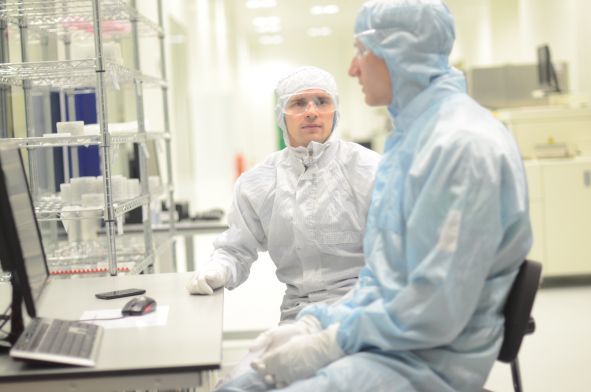
A video of this event can be viewed here . It should be noted that the actual production of products has not yet been launched, so there are allowances in overalls.
Dutch period
From the completion of the construction of the factory, we are transferred in four coordinates: from Moscow to Delft and back in time - in 2013, more precisely, to its beginning. The factory in Moscow is only at the design stage, but work in Delft is already in full swing - by the time the construction is completed, the factory should be equipped with both equipment and qualified personnel. The preparation of both is happening in Holland, in Delft.
Let us briefly dwell on the technology available in Mapper Lithography at the time of the creation of Mapper LLC. As noted above, Mapper Lithography was born within the walls of the Delft Technical University and, accordingly, has always had close ties with it. Therefore, when the question arose of manufacturing MEMS elements of electronic optics, the clean rooms of the university were the natural choice, but now the university technology was to be transferred to production.
Thus, we faced the following task: to understand the existing university technology, shift it to the production rails and select appropriate equipment for these production tasks. If the university technology was developed according to the principle “we use the equipment we have”, our technology was built according to the principle “we buy the equipment we need to get a high-quality end result”.
When choosing equipment, my experience came in very handy - 15 years of work in European semiconductor R & D and manufacturing - first at the IMEC research center in Belgium, then at the GlobalFoundries factory (former AMD plant) in Germany. Equipment was chosen carefully: first, equipment requirements were prepared, discussed and approved, potential suppliers were located (usually 2-3 companies), demonstration experiments were conducted (usually with a visit to the equipment supplier company), then a supplier was selected from several companies on the basis of compliance with the requirements impressions from the company and the price of equipment. It should be noted that in the first place was compliance, not price. Thus, the deep etching installation for silicon was bought by the most expensive on the market (competitors cost twice as cheap) since it only met the strict requirements for the production of elements. In addition, the manufacturer specialized in the manufacture of equipment for production, while the competitor - in the manufacture of equipment for universities and research centers. On the other hand, despite the lack of compromise in the field of quality, by optimizing the equipment line and competent bidding with several potential suppliers, all equipment was purchased not so much as the budget was exceeded, but even with 15% savings (I note that the money saved was spent on the construction of clean rooms, as they, just, cost more than originally planned).
In parallel with the selection and purchase of equipment, our engineers were trained in Mapper Lithography. Since the equipment we purchased was basically different from what was available in Delft, the goal was not to learn how to work with the equipment, but to understand what should come out as an end product. In addition, it was necessary to understand the business processes used in the parent company - how reports are made, how decisions are made, etc.
Much attention has been paid to planning the launch of the factory. For each piece of equipment, a list of necessary actions was compiled (several hundred points each) —as pilots had before take-off — that needed to be completed before the equipment was ready for operation. As a result, careful planning paid off - all equipment deliveries were completed on time, the equipment launch took about two months (with the exception of certain pieces of equipment that had bad predictable problems like the manufacturer’s bankruptcy).
At the time of my arrival at the company (May 2013) there were three engineers, the chief accountant and the general director. By the time the factory was launched (May 2014), Mapper consisted of 15 engineers trained in Holland.
Run factory
Thanks to careful planning, the launch of the factory took place without any special excesses, except for the bankruptcy of one of the equipment manufacturers - it’s good that he managed to produce and partially launch the equipment, but had to finish it himself with the help of third-party companies.
The team's well-coordinated work allowed the first silicon cell (projection electron lens) to be produced in August 2014. 4 months have passed since the first process unit was unpacked.
Today - factory opportunities

Today, our factory is almost a complete production line for the manufacture of modern MEMS on 100 mm plates. We have the following technological capabilities:
- Lithography (resolution up to 300 nm, the possibility of combining the front and back sides of the plate)
- plasma chemical etching (including Bosch deep etching)
- deposition of dielectric and metal films
- high temperature oxidation
- liquid chemical treatment
- metrology (both standard and specialized, developed by Mapper Lithography)
Almost all installations are robotic - the plates from the cassette are fed for processing by robots.
We have mastered the production of almost all the elements of electronic optics needed for Mapper Lithogrpahy, now we are developing a process technology for the last remaining element - the electrode controlling the electron beams. The electrode itself is produced by a contract manufacturer of plates, our task is to etch with high precision through holes for the passage of electron beams without damaging the original chip.
The initial hopes that our factory will be able to manufacture some products in addition to the elements of electronic optics for the head company have not been justified. The demand on the Russian market is extremely low, and besides, the contract manufacturers of plates, which we are, are not in demand - everyone needs ready-made appliances, and there are no companies that can make such devices from ready-made plates. But this is a topic for a separate article. So far, in addition to our main orders, we have produced only one batch of accelerometers from 10 plates.
Conclusion
We often hear: "Well, you launched your microscopic factory, created 30 jobs, for our economy it is a drop in the ocean." In principle, yes, from the point of view of the Russian economy, we are insignificant. But our merit is different. By our example, we showed that in Russia it is quite possible to create high-tech production of the European level. That money is not stolen and the launch will not drag on for many years. That the Russian company can work with high quality fulfilling all contractual obligations on time. That the inscription "Made in Russia" can cause not a wry smile, but pride.
Source: https://habr.com/ru/post/392983/
All Articles