Goodbye reading heads! Or how flash memory works
Hi, Geektimes! We often talk about the benefits of SSD, debunking the myths about solid-state drives, just recently, we have been in production. But how does flash memory actually work? What is the difference between different types of NAND? All those wishing to understand these issues are welcome under the cat.
Before we begin our conversation, let's briefly recall the hard drives. As is known, the latter store information on several magnetic plates, which are popularly called platters. In a simplified form, the actuator with reading heads receives information, and the disk rotates all the time to complete the read / write processes. It hardly makes sense to stop here for a long time, but it is important to capture the essence.
Since the disk head block must coincide with a certain area (track) for reading or writing data, and the disk rotates constantly, it takes some time before they can access the information and the sector will be under the head, especially if the requests are chaotic. And although the HDD delay is measured in milliseconds, this is enough to make the CPU wait, the delay of which is measured in nanoseconds. In one millisecond, one million nanoseconds, and on average a hard disk needs from 10 to 15 milliseconds to search for information and start reading it. Yes, now there are solutions whose rotational speed reaches 15 thousand revolutions per minute, but even the fastest HDD will not be as fast as we would like.
')
Maybe we would be content with “very” fast HDDs (as Henry Ford said: “if I asked people what they wanted, they would ask me to create fast horses”), but the manufacturers of drives, among which are yours humble servant, the benefit does not stand still . Appeared SSD (Solid-state drives or solid-state drives), where information is not stored on rotating disks, but with the help of NAND flash memory. We will dwell on it in detail.
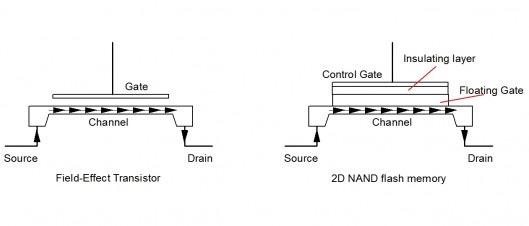
In the case of NAND, the information is stored in an array of memory cells — these are floating gate transistors. Depending on the direction of the voltage, the electrons move between the Control Gate (control gate) and the NAND channel.
As soon as voltage is applied to the control gate, the electrons begin to be attracted upwards - the resulting electric field helps them to reach the floating gate, overcoming an oxide obstacle. The latter acts as an insulator, since it is thanks to him that the electrons do not move further than the floating gate. This is how cell programming occurs.
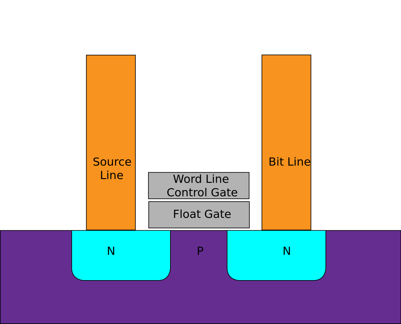
The process of erasing the cell looks exactly the opposite - the voltage is applied to the channel, the electrons are moved from the floating gate through the oxide back by grounding the control gate.
The cell with one transistor operates as follows. Depending on the presence or absence of a charge on the floating gate, the state of the transistor is determined - whether it is open or closed. When considering the supply voltage to the control gate as the initialization of the memory cell, it is possible to judge whether there is a charge on the floating gate by the voltage between the source and the drain. If you place an electron on the floating gate and apply voltage to the control gate, the transistor will be closed. Get a memory cell that is capable of storing one bit. When using the hot-electron injection method, a voltage is applied to the drain and the control gate, which causes electrons to move through the barrier.
A cell with two transistors is a modification of a single-transistor. In this case, the transistor (normal) isolates the bit line from the floating gate transistor.
The charge is removed from the floating gate by applying a negative voltage to the control gate (a positive voltage is applied to the source). As a result, we have the Fowler – Nordheim tunneling: electrons move (tunnel) from the area of the floating gate to the source.
Rewrite cycle Before programming a new cell with new electrons, you must first clean the old ones. In practice, most users do not have to pay attention to the number of rewriting cycles, because the SSD resource is easily enough for any amount of recorded data. True, there are annoying exceptions, but this is what the manufacturer’s warranty is for .
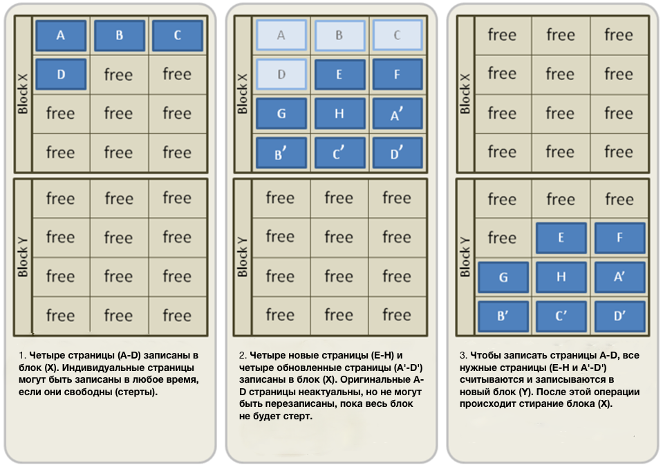
In solid-state drives, flash memory consists of blocks, and the latter are made up of pages. Information is recorded in these pages, and to update the data it is not enough to simply overwrite irrelevant pages. So, first the data is moved from the old pages to the new ones, then sent to another block, and only after that the block is deleted with irrelevant data. Once the block is erased, it will be free to write new data. Such a tricky process - in a visual format, it seems much more understandable.
Obviously, the absence of moving disks (and indeed moving parts) is one of the main advantages of SSD over hard disks, and this is what makes solid-state drives work at speeds that are noticeably superior to HDD. For clarity, here is a summary table of the latency times of various types of NAND and HDD.
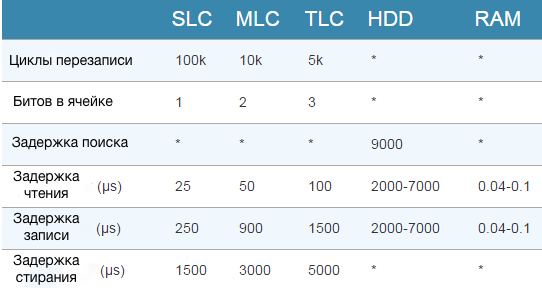
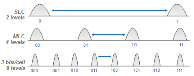
SLC, MLC, TLC are not just abbreviations, they denote the number of bits in each cell. For SLC (Single) it is one bit, for MLC (Multi) - two bits, for TLC (Triple) - respectively, three bits. Due to this, the MLC stores twice as much information as the SLC, and this despite the fact that the number of cells is the same. In general, the principle of operation for these types of NAND is the same, which cannot be said about endurance.
For a certain time, the physical structure of the cells may be subject to wear by reducing the oxide layer caused by the activity of the electrons. As a result, the electrons accumulate a negative charge and get stuck, a higher voltage is applied, the oxide layer decreases again. Such a vicious circle is obtained.
SLC, MLC and TLC differ in endurance. If, for example, we take a 16 Gbps NAND crystal, we get a 16 Gbps SLC, with one bit in each cell. Accordingly, it will be 32 Gbps for the MLC and 48 Gbps for the TLC. However, in the latter case, the NAND crystal still has to be cut, as a result, the equivalent of 32 Gbps for the MLC is obtained. Who do you think can withstand the biggest changes in tension?
With two levels (0.1), SLC in this parameter is the best indicator - this type of NAND withstands a wide range of voltage fluctuations. With increasing levels, this range decreases, so TLC with its 8 levels and 3 bits in the cell has the smallest number of rewrite cycles.
Since the reduction of the crystal has long been a problem, to replace the modern planar flash NAND comes 3D NAND. It is less susceptible to wear due to the absence of the need to supply high voltage when writing data to the cell. Manufacturers are actively developing this area and give the technology their own names (for Samsung - 3D V-NAND, for Toshiba - BiCS 3D NAND, and so on). The point is that in this case we get a cylinder with the upper layer in the role of the control gate, while the inner layer acts as an insulator. The cells themselves are located under each other, forming a stack. The control logic is located under the memory array, the chip area is freed, where subsequently the “home” of the memory cell is found.

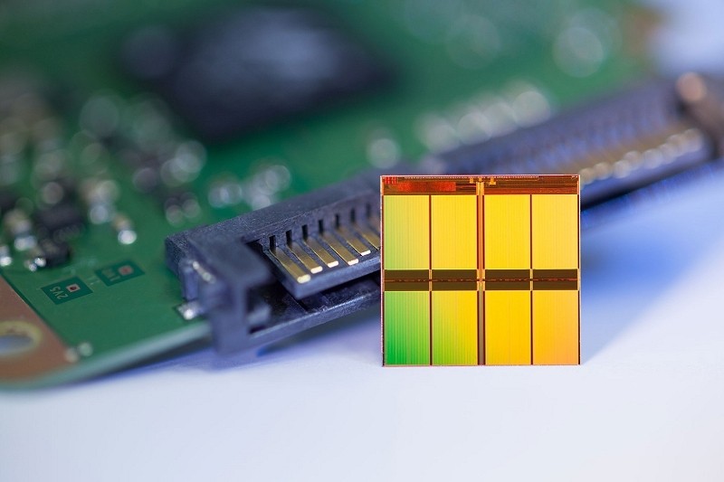
All of the above, we cannot observe on our own (at least without special equipment). And this is how it all looks after the manufacture of printed circuit boards, soldering, installation of chips and microcircuits:
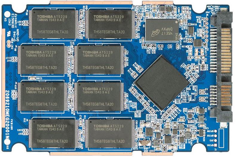
OCZ Trion 150
Here we see both the flash memory chips and the buffer and the controller, carefully covered with a thermal cutter. Yes, the topic is not about the SSD device, but the operation of flash memory, but there is nowhere without a controller. And that's why.
The controller distributes the entry to the flash memory cells, “directs” the reading from the memory cells and TRIM (more on that later) - in general, the phrase “we don't have the irreplaceable” is not about it. It is he who controls the transfer of data, both on SATA and PCIe, distributes information over NAND for less wear. Without the help of the firmware, of course, is not enough.
The controller is connected to the flash memory in parallel and, as you can see, it performs one of the key roles. The Trion 150, for example, uses a Toshiba controller, while the Vertex 460A 0 already uses the Barefoot 3 M10 from OCZ.
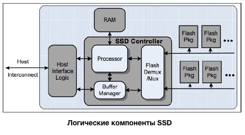
Oh yeah, I almost forgot about the cache. It is a reliable controller satellite: as soon as a command is given to change the file on the SSD, the unit first gets into the cache memory, where the change occurs. At this time, irrelevant data in NAND is deleted, and the controller finds where to put the information that was placed in the buffer. The main principle is to select the cell with the least wear, which is what the controller does; after its command, the changed data is sent to the new “home”.
Now most SSDs, including those from OCZ, also support TRIM, a special technology that marks out irrelevant data. In this case, unnecessary information is not recorded in other memory blocks, which favorably affects not only the number of rewriting cycles, but also the write speed itself.
Obviously, compared to conventional hard disks, NAND is a real breakthrough, but it also has its own problems and shortcomings. Yes, NAND has great prospects in terms of storage capacity, but the price per gigabyte leaves much to be desired. It is unlikely that in the near future this parameter will succeed in “catching” hard drives.
Due to the use of SLC-caches and fast data standards, SSDs have become even more productive, have good bandwidth. Nevertheless, in the long run, it is assumed that something else will come to replace NAND. And in fact, 3D NAND - the first "bell", which testifies to this.
Now NAND, of course, on horseback - as they say, true king of the hill. And it will remain this king for at least the next 4-5 years.
A look into the past
Before we begin our conversation, let's briefly recall the hard drives. As is known, the latter store information on several magnetic plates, which are popularly called platters. In a simplified form, the actuator with reading heads receives information, and the disk rotates all the time to complete the read / write processes. It hardly makes sense to stop here for a long time, but it is important to capture the essence.
Since the disk head block must coincide with a certain area (track) for reading or writing data, and the disk rotates constantly, it takes some time before they can access the information and the sector will be under the head, especially if the requests are chaotic. And although the HDD delay is measured in milliseconds, this is enough to make the CPU wait, the delay of which is measured in nanoseconds. In one millisecond, one million nanoseconds, and on average a hard disk needs from 10 to 15 milliseconds to search for information and start reading it. Yes, now there are solutions whose rotational speed reaches 15 thousand revolutions per minute, but even the fastest HDD will not be as fast as we would like.
')
Some theory
Maybe we would be content with “very” fast HDDs (as Henry Ford said: “if I asked people what they wanted, they would ask me to create fast horses”), but the manufacturers of drives, among which are yours humble servant, the benefit does not stand still . Appeared SSD (Solid-state drives or solid-state drives), where information is not stored on rotating disks, but with the help of NAND flash memory. We will dwell on it in detail.
In the case of NAND, the information is stored in an array of memory cells — these are floating gate transistors. Depending on the direction of the voltage, the electrons move between the Control Gate (control gate) and the NAND channel.
As soon as voltage is applied to the control gate, the electrons begin to be attracted upwards - the resulting electric field helps them to reach the floating gate, overcoming an oxide obstacle. The latter acts as an insulator, since it is thanks to him that the electrons do not move further than the floating gate. This is how cell programming occurs.
The process of erasing the cell looks exactly the opposite - the voltage is applied to the channel, the electrons are moved from the floating gate through the oxide back by grounding the control gate.
The cell with one transistor operates as follows. Depending on the presence or absence of a charge on the floating gate, the state of the transistor is determined - whether it is open or closed. When considering the supply voltage to the control gate as the initialization of the memory cell, it is possible to judge whether there is a charge on the floating gate by the voltage between the source and the drain. If you place an electron on the floating gate and apply voltage to the control gate, the transistor will be closed. Get a memory cell that is capable of storing one bit. When using the hot-electron injection method, a voltage is applied to the drain and the control gate, which causes electrons to move through the barrier.
A cell with two transistors is a modification of a single-transistor. In this case, the transistor (normal) isolates the bit line from the floating gate transistor.
The charge is removed from the floating gate by applying a negative voltage to the control gate (a positive voltage is applied to the source). As a result, we have the Fowler – Nordheim tunneling: electrons move (tunnel) from the area of the floating gate to the source.
Rewrite cycle Before programming a new cell with new electrons, you must first clean the old ones. In practice, most users do not have to pay attention to the number of rewriting cycles, because the SSD resource is easily enough for any amount of recorded data. True, there are annoying exceptions, but this is what the manufacturer’s warranty is for .
In solid-state drives, flash memory consists of blocks, and the latter are made up of pages. Information is recorded in these pages, and to update the data it is not enough to simply overwrite irrelevant pages. So, first the data is moved from the old pages to the new ones, then sent to another block, and only after that the block is deleted with irrelevant data. Once the block is erased, it will be free to write new data. Such a tricky process - in a visual format, it seems much more understandable.
Obviously, the absence of moving disks (and indeed moving parts) is one of the main advantages of SSD over hard disks, and this is what makes solid-state drives work at speeds that are noticeably superior to HDD. For clarity, here is a summary table of the latency times of various types of NAND and HDD.
SLC, MLC, TLC are not just abbreviations, they denote the number of bits in each cell. For SLC (Single) it is one bit, for MLC (Multi) - two bits, for TLC (Triple) - respectively, three bits. Due to this, the MLC stores twice as much information as the SLC, and this despite the fact that the number of cells is the same. In general, the principle of operation for these types of NAND is the same, which cannot be said about endurance.
For a certain time, the physical structure of the cells may be subject to wear by reducing the oxide layer caused by the activity of the electrons. As a result, the electrons accumulate a negative charge and get stuck, a higher voltage is applied, the oxide layer decreases again. Such a vicious circle is obtained.
SLC, MLC and TLC differ in endurance. If, for example, we take a 16 Gbps NAND crystal, we get a 16 Gbps SLC, with one bit in each cell. Accordingly, it will be 32 Gbps for the MLC and 48 Gbps for the TLC. However, in the latter case, the NAND crystal still has to be cut, as a result, the equivalent of 32 Gbps for the MLC is obtained. Who do you think can withstand the biggest changes in tension?
With two levels (0.1), SLC in this parameter is the best indicator - this type of NAND withstands a wide range of voltage fluctuations. With increasing levels, this range decreases, so TLC with its 8 levels and 3 bits in the cell has the smallest number of rewrite cycles.
Since the reduction of the crystal has long been a problem, to replace the modern planar flash NAND comes 3D NAND. It is less susceptible to wear due to the absence of the need to supply high voltage when writing data to the cell. Manufacturers are actively developing this area and give the technology their own names (for Samsung - 3D V-NAND, for Toshiba - BiCS 3D NAND, and so on). The point is that in this case we get a cylinder with the upper layer in the role of the control gate, while the inner layer acts as an insulator. The cells themselves are located under each other, forming a stack. The control logic is located under the memory array, the chip area is freed, where subsequently the “home” of the memory cell is found.
Some practice
All of the above, we cannot observe on our own (at least without special equipment). And this is how it all looks after the manufacture of printed circuit boards, soldering, installation of chips and microcircuits:
OCZ Trion 150
Here we see both the flash memory chips and the buffer and the controller, carefully covered with a thermal cutter. Yes, the topic is not about the SSD device, but the operation of flash memory, but there is nowhere without a controller. And that's why.
The controller distributes the entry to the flash memory cells, “directs” the reading from the memory cells and TRIM (more on that later) - in general, the phrase “we don't have the irreplaceable” is not about it. It is he who controls the transfer of data, both on SATA and PCIe, distributes information over NAND for less wear. Without the help of the firmware, of course, is not enough.
The controller is connected to the flash memory in parallel and, as you can see, it performs one of the key roles. The Trion 150, for example, uses a Toshiba controller, while the Vertex 460A 0 already uses the Barefoot 3 M10 from OCZ.
Oh yeah, I almost forgot about the cache. It is a reliable controller satellite: as soon as a command is given to change the file on the SSD, the unit first gets into the cache memory, where the change occurs. At this time, irrelevant data in NAND is deleted, and the controller finds where to put the information that was placed in the buffer. The main principle is to select the cell with the least wear, which is what the controller does; after its command, the changed data is sent to the new “home”.
Now most SSDs, including those from OCZ, also support TRIM, a special technology that marks out irrelevant data. In this case, unnecessary information is not recorded in other memory blocks, which favorably affects not only the number of rewriting cycles, but also the write speed itself.
Minute of philosophy
Obviously, compared to conventional hard disks, NAND is a real breakthrough, but it also has its own problems and shortcomings. Yes, NAND has great prospects in terms of storage capacity, but the price per gigabyte leaves much to be desired. It is unlikely that in the near future this parameter will succeed in “catching” hard drives.
Due to the use of SLC-caches and fast data standards, SSDs have become even more productive, have good bandwidth. Nevertheless, in the long run, it is assumed that something else will come to replace NAND. And in fact, 3D NAND - the first "bell", which testifies to this.
Now NAND, of course, on horseback - as they say, true king of the hill. And it will remain this king for at least the next 4-5 years.
Source: https://habr.com/ru/post/392891/
All Articles