The history of the development of processors: the late 80s - early 2000s
Continuing the theme of the first article - the history of the evolution of processors from the late 20th century to the early 21st century.
Many processors of the 1980s used CISC (complex instruction set computing) architecture. The chips were quite complex and expensive, and also not productive enough. There was a need to modernize production and increase the number of transistors.
RISC Architecture
')
In 1980, the Berkeley RISC project was launched, led by American engineers David Patterson and Carlo Secwin. RISC (restricted instruction set computer) - processor architecture with increased speed due to simplified instructions.
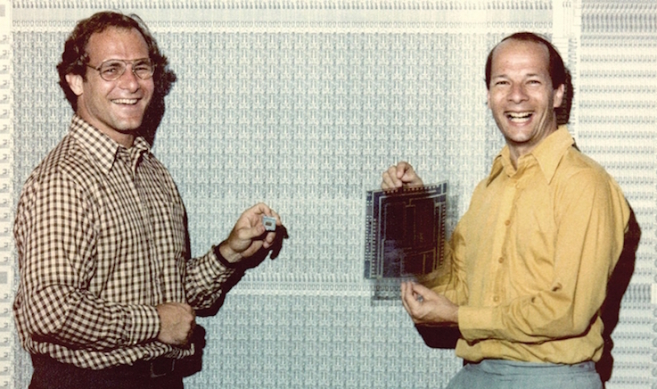
Berkeley RISC Project Leaders - David Patterson and Carlo Secqueen
After several years of fruitful work, several samples of processors with a reduced instruction set appeared on the market. Each instruction of the RISC platform was simple and was executed in one clock cycle. There were also a lot more general registers. In addition, pipelining with simplified commands was used, which made it possible to effectively increase the clock frequency.
RISC I was released in 1982 and contained more than 44,420 transistors. He had only 32 instructions and worked at 4 MHz. The next RISC II was 40,760 transistors, used 39 instructions and was faster.

RISC II processor
MIPS processors: R2000, R3000, R4000 and R4400
The architecture of MIPS processors (Microprocessor without Interlocked Pipeline Stages) provided for the presence of auxiliary units in the composition of the crystal. In MIPS, an elongated conveyor was used.
In 1984, a group of researchers led by American scientist John Hennessy founded a company that designs microelectronic devices. MIPS licensed the microprocessor architecture and IP cores for smart home devices, network and mobile applications. In 1985, the first product of the company was released - 32-bit R2000, which in 1988 was finalized in the R3000. The updated model had support for multiprocessing, instruction cache and data. The processor has found application in the SG-series of workstations of different companies. Also, the R3000 became the basis of the Sony PlayStation gaming console.

R3000 processor
In 1991, the new generation R4000 lineup was released. This processor had a 64-bit architecture, built-in co-processor and worked at a clock frequency of 100 MHz. The internal cache was 16 KB (8 KB cache commands and 8 KB cache data).
A year later, there was a modified version of the processor - R4400. In this model, the cache increased to 32 KB (16 KB cache commands and 16 KB cache data). The processor could operate at a frequency of 100 MHz - 250 MHz.
MIPS processors: R8000 and R10000
In 1994, the first processor appeared with a superscalar implementation of the MIPS architecture - R8000. The capacity of the data cache was 16 Kb. This CPU had a high data access bandwidth (up to 1.2 Gb / s) in combination with a high speed of operations. The frequency reached 75 MHz - 90 MHz. 6 schemes were used: a device for integer commands, for commands with a floating comma, three secondary descriptors of the RAM memory cache and an ASIC cache controller.

R8000 processor
In 1996, a revised version was released - R10000. The processor included 32 KB of primary data and instruction cache. The CPU worked at a frequency of 150 MHz - 250 MHz.
In the late 90s, MIPS started selling licenses for 32-bit and 64-bit MIPS32 and MIPS64 architectures.
SPARC processors
Processors ranked with products from Sun Microsystems, which developed the scalable architecture SPARC (Scalable Processor Architecture). The first processor of the same name was released in the late 80s and was named SPARC V7. Its frequency reached 14.28 MHz - 40 MHz.
In 1992, the next 32-bit version appeared, called SPARC V8, on the basis of which the microSPARC processor was created. The clock frequency was 40 MHz - 50 MHz.
Texas Instruments, Fujitsu, Philips and others have worked together to create the next generation of SPARC V9 architecture with Sun Microsystems. The platform expanded to 64 bits and was superscalar with a 9-step pipeline. SPARC V9 involved the use of a first-level cache, divided into instructions and data (each 16 KB in size), as well as a second level with a capacity of 512 KB - 1024 KB.

UltraSPARC III processor
StrongARM processors
In 1995, a project started to develop the StrongARM microprocessor family, which implemented the ARM V4 instruction set. These CPUs were a classic scalar architecture with a 5-step pipeline, including memory management units and supporting instruction and data cache of 16 KB each.

StrongARM SA-110
And in 1996, the first StrongARM processor, the SA-110, was released. He worked at clock frequencies of 100 MHz, 160 MHz or 200 MHz.
The SA-1100, SA-1110 and SA-1500 models also entered the market.

SA-110 processor in Apple MessagePad 2000
POWER, POWER2 and PowerPC processors
In 1985, IBM began developing the next-generation RISC architecture as part of the America Project. The development of the POWER processor (Performance Optimization With Enhanced RISC) and a set of instructions for it lasted 5 years. It was very productive, but consisted of 11 different microcircuits. And so in 1992 came another version of the processor that fit in one chip.

POWER Chipset
In 1991, the joint efforts of the IBM, Apple and Motorola alliance developed the PowerPC architecture (abbreviated as PPC). It consisted of the basic set of functions of the POWER platform, and also supported work in two modes and was backward compatible with the 32-bit mode of operation for the 64-bit version. The main purpose was personal computers.
The PowerPC 601 processor was used in Macintosh.

PowerPC processor
In 1993, POWER2 was introduced with an expanded set of commands. The processor clock frequency ranged from 55 MHz to 71.5 MHz, while the data and instructions cache was 128-256 Kb and 32 Kb. The processor chips (there were 8 of them) contained 23 million transistors, and it was made using 0.72 micro CMOS technology.
In 1998, IBM launched the third 64-bit POWER3 processor series, fully compatible with the PowerPC standard.
From 2001 to 2010, POWER4 models (up to eight concurrently executed commands), dual-core POWER5 and POWER6, four-eight nuclear POWER7 came out.
Alpha 21064A Processors
In 1992, Digital Equipment Corporation (DEC) released an Alpha 21064 (EV4) processor. It was a 64-bit superscalar crystal with a pipeline architecture and a clock frequency of 100 MHz - 200 MHz. Made on a 0.75-micron process technology, with an external 128-bit processor bus. There were 16 KB of cache memory (8 KB of data and 8 KB of instructions).
The next model in the series was the processor 21164 (EV5), which was released in 1995. He had two integer blocks and already counted three levels of cache memory (two in the processor, the third - external). The cache of the first level was divided into data cache and instruction cache of 8 KB each. The amount of cache memory of the second level was 96 KB. CPU clock speeds ranged from 266 MHz to 500 MHz.

DEC Alpha AXP 21064
In 1996, the Alpha 21264 (EV6) processor came out with 15.2 million transistors manufactured using a 15.2-micron process technology. Their clock frequency ranged from 450 MHz to 600 MHz. The integer blocks and the load / save blocks were combined into a single Ebox module, and the floating-point computing blocks were combined into a Fbox module. The first level cache retained the separation of memory for instructions and for data. The volume of each part was 64 Kb. The cache size of the second level was from 2 MB to 8 MB.
In 1999, DEC was bought by Compaq. As a result, most of the production of products that used Alpha was transferred to API company NetWorks, Inc.
Intel P5 and P54C processors
According to the Vinod Dhama model, a fifth-generation processor codenamed P5 was developed. In 1993, the CPU went into production under the name Pentium.
The P5 core processors were manufactured using 800-nanometer process technology using bipolar BiCMOS technology. They contained 3.1 million transistors. The Pentium had a 64-bit data bus, superscalar architecture. There was a separate caching of program code and data. The first-level cache memory of 16 KB was used, divided into 2 segments (8 KB for data and 8 KB for instructions). The first models were with frequencies of 60 MHz - 66 MHz.

Intel Pentium processor
In the same year, Intel launched the P54C processors. The production of new processors was transferred to the 0.6-micron process technology. The speed of the processor was 75 MHz, and since 1994 - 90 MHz and 100 MHz. A year later, the P54C (P54CS) architecture was transferred to the 350-nm process technology and the clock frequency increased to 200 MHz.
In 1997, the P5 received the latest update - P55C (Pentium MMX). MMX (MultiMedia eXtension) instruction set support has been added. The processor consisted of 4.5 million transistors and is manufactured using an advanced 280-nanometer CMOS technology. The size of cache memory of the first level increased to 32 KB (16 KB for data and 16 KB for instructions). The processor frequency has reached 233 MHz.
AMD K5 and K6 processors
In 1995, AMD released the K5 processor. The architecture was a RISC core, but it worked with complex CISC instructions. The processors were manufactured using a 350- or 500-nanometer process technology, with 4.3 million transistors. All K5 had five integer blocks and one floating point unit. The instruction cache size was 16 Kb, and the data - 8 Kb. Processor clock speeds ranged from 75 MHz to 133 MHz.

AMD K5 processor
Under the K5 brand, there were two variants of SSA / 5 and 5k86 processors. The first one worked at frequencies from 75 MHz to 100 MHz. The 5k86 processor operated at frequencies from 90 MHz to 133 MHz.
In 1997, the company introduced the K6 processor, whose architecture was significantly different from the K5. The processors were manufactured using a 350-nanometer process technology, included 8.8 million transistors, supported changing the order of instructions execution, a set of MMX commands and a floating-point computing unit. The crystal area was 162 mm². The cache of the first level consisted of 64 Kb (32 Kb of data and 32 Kb of instructions). The processor worked at 166 MHz, 200 MHz and 233 MHz. The system bus frequency was 66 MHz.
In 1998, AMD released chips with an improved K6-2 architecture, with 9.3 million transistors manufactured using the 250-nanometer process technology. The maximum frequency of the chip was 550 MHz.

AMD K6 processor
In 1999, the third generation was released - architecture K6-III. Crystal retained all the features of K6-2, but at the same time a built-in cache memory of the second level of 256 KB appeared. The cache of the first level was 64 Kb.
AMD K7 processors
Also in 1999, the K7 came to replace the K6. They were released on the 250-nm technology with 22 million transistors. The CPU had a new unit of integer calculations (ALU). The EV6 system bus provided data transfer on both clock fronts, which made it possible to obtain an effective frequency of 200 MHz at a physical frequency of 100 MHz. The cache of the first level was 128 Kb (64 Kb of instructions and 64 Kb of data). The second level cache reached 512 Kb.

AMD K7 processor
Somewhat later, crystals based on the Orion core appeared. They were made on the 180-nm process technology.
The release of the Thunderbird core has made unusual changes to the processors. Level 2 cache memory was transferred directly to the processor core and worked at the same frequency as it. The cache was with an effective volume of 384 KB (128 KB cache of the first level and 256 KB cache of the second level). The system bus clock frequency has increased - now it functioned at 133 MHz.
Intel P6 processors
The P6 architecture replaced the P5 in 1995. The processor was superscalar and supported changes in the order of operations. The processors used dual independent bus, which significantly increased memory bandwidth.
Also in 1995, the next-generation Pentium Pro processors were introduced. The crystals worked at a frequency of 150 MHz - 200 MHz, had 16 KB of cache memory of the first level and up to 1 MB of cache in the second level.

Intel Pentium Pro processor
In 1999, the first Pentium III processors were introduced. They were based on the new P6 core generation called Katmai, which were modified versions of Deschutes. Support for SSE instructions has been added to the kernel, as well as an improved memory handling mechanism. The clock frequency of Katmai processors reached 600 MHz.
In 2000, the first Pentium 4 processors with the Willamette core came out. The effective system bus frequency was 400 MHz (physical frequency - 100 MHz). The cache data of the first level reached the volume of 8 KB, and the cache memory of the second level - 256 KB.
The next core of the line was Northwood (2002). The processors contained 55 million transistors and were manufactured using the new 130 nm CMOS technology with copper connections. The system bus frequency was 400 MHz, 533 MHz or 800 MHz.

Intel Pentium 4
In 2004, the production of processors was again transferred to more subtle technological standards - 90 nm. Pentium 4 came out on Prescott core. The data cache of the first level increased to 16 KB, and the cache of the second level reached 1 MB. The clock frequency was 2.4 GHz - 3.8 GHz, the system bus frequency - 533 MHz or 800 MHz.
The latest core used in Pentium 4 processors was the single core Cedar Mill. Produced by the new process technology - 65 nm. There were four models: 631 (3 GHz), 641 (3.2 GHz), 651 (3.4 GHz), 661 (3.6 GHz).
Processors Athlon 64 and Athlon 64 X2
At the end of 2003, AMD released a new 64-bit K8 architecture, built on a 130-nanometer process technology. The processor had a built-in memory controller and a HyperTransport bus. She worked at 200 MHz. The new AMD products are called Athlon 64. The processors supported many instruction sets, such as MMX, 3DNow !, SSE, SSE2 and SSE3.

Athlon 64 processor
In 2005, AMD processors called the Athlon 64 X2 entered the market. These were the first dual-core processors for desktop computers. The model was based on two cores made on a single crystal. They had a shared memory controller, a HyperTransport bus and a queue of commands.

Processor Athlon 64 X2
During 2005 and 2006, AMD launched four generations of dual-core chips: three 90-nm cores Manchester, Toledo and Windsor, as well as the 65-nm core Brisbane. The processors differed in the volume of second-level cache and power consumption.
Intel Core Processors
Pentium M processors provided better performance than desktop processors based on NetBurst microarchitecture. And therefore, their architectural solutions became the basis for the Core microarchitecture, which was published in 2006. The first desktop quad-core processor was the Intel Core 2 Extreme QX6700 with a clock speed of 2.67 GHz and 8 MB of second-level cache.
The code name of the first generation of Intel mobile processors was Yonah. They were produced using a 65 nm process technology, based on the Banias / Dothan Pentium M architecture, with the LaGrande protection technology added. The processor could process up to four instructions per clock. In Core, the algorithm for processing 128-bit SSE, SSE2, and SSE3 instructions has been redesigned. If earlier each team was processed in two cycles, now the operation required only one cycle.

Intel Core 2 Extreme QX6700
In 2007, the 45-nm Penryn microarchitecture came out using lead-free Hi-k metal gates. The technology has been used in the Intel Core 2 Duo processor family. Support for SSE4 instructions has been added to the architecture, and the maximum size of the Level 2 cache in dual-core processors has increased from 4 MB to 6 MB.
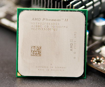
AMD Phenom II X6 Processor
In 2008, the next-generation architecture came out - Nehalem. The processors have an integrated memory controller that supports 2 or 3 DDR3 SDRAM channels or 4 FB-DIMM channels. Replaced the FSB bus, a new QPI bus has arrived. The level 2 cache is reduced to 256 KB per core.
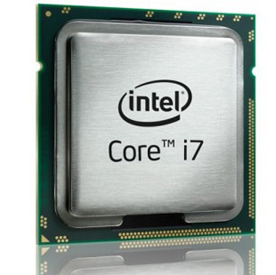
Intel Core i7
Intel soon transferred the Nehalem architecture to a new 32-nm process technology. This line of processors is called Westmere.
The first model of the new microarchitecture was Clarkdale, which has two cores and an integrated graphics core, produced according to the 45-nm process technology.
AMD K10 processors
AMD tried to keep up with Intel. In 2007, she released the x86 - K10 microprocessor architecture generation. Four processor cores were combined on a single chip. In addition to the 1 st and 2 nd level cache, the K10 models finally got L3 with a capacity of 2 MB. The size of the data cache and instructions of the 1st level was 64 KB each, and the cache memory of the 2nd level - 512 KB. Also appeared promising support for the DDR3 memory controller. K10 used two 64-bit controllers. Each processor core had a 128-bit floating point unit. On top of that, the new processors worked through the HyperTransport 3.0 interface.
In 2007, with the K10 architecture, AMD's multi-core Phenom CPUs were designed for use in stationary personal computers. Solutions based on the K10 were made on the 65- and 45-nm process technology. In the new version of the architecture (K10, 5), the memory controller worked with DDR2 and DDR3 memory.

AMD Phenom Processor
In 2011, the new Bulldozer architecture was released. Each module contained two cores with its own block of integer calculations and 1 st level cache memory. The supported support was Level 3 cache with a capacity of 8 MB, HyperTransport 3.1 bus, technologies for increasing the frequency of second-generation Turbo Core cores and AVX, SSE 4.1, SSE 4.2, AES instruction sets. Also, Bulldozer processors were endowed with a dual-channel DDR3 memory controller with an effective frequency of 1866 MHz.

AMD Bulldozer Processor
In 2013, the company introduced the next generation of processors - Piledriver. This model was an enhanced Bulldozer architecture. Branches prediction units were improved, the performance of the floating point and integer calculations module, as well as the clock frequency, increased.
Looking through the history, you can trace the stages of development of processors, changes in their architecture, improvements in development technologies and much more. CPU , , .
Many processors of the 1980s used CISC (complex instruction set computing) architecture. The chips were quite complex and expensive, and also not productive enough. There was a need to modernize production and increase the number of transistors.
RISC Architecture
')
In 1980, the Berkeley RISC project was launched, led by American engineers David Patterson and Carlo Secwin. RISC (restricted instruction set computer) - processor architecture with increased speed due to simplified instructions.
Berkeley RISC Project Leaders - David Patterson and Carlo Secqueen
After several years of fruitful work, several samples of processors with a reduced instruction set appeared on the market. Each instruction of the RISC platform was simple and was executed in one clock cycle. There were also a lot more general registers. In addition, pipelining with simplified commands was used, which made it possible to effectively increase the clock frequency.
RISC I was released in 1982 and contained more than 44,420 transistors. He had only 32 instructions and worked at 4 MHz. The next RISC II was 40,760 transistors, used 39 instructions and was faster.
RISC II processor
MIPS processors: R2000, R3000, R4000 and R4400
The architecture of MIPS processors (Microprocessor without Interlocked Pipeline Stages) provided for the presence of auxiliary units in the composition of the crystal. In MIPS, an elongated conveyor was used.
In 1984, a group of researchers led by American scientist John Hennessy founded a company that designs microelectronic devices. MIPS licensed the microprocessor architecture and IP cores for smart home devices, network and mobile applications. In 1985, the first product of the company was released - 32-bit R2000, which in 1988 was finalized in the R3000. The updated model had support for multiprocessing, instruction cache and data. The processor has found application in the SG-series of workstations of different companies. Also, the R3000 became the basis of the Sony PlayStation gaming console.
R3000 processor
In 1991, the new generation R4000 lineup was released. This processor had a 64-bit architecture, built-in co-processor and worked at a clock frequency of 100 MHz. The internal cache was 16 KB (8 KB cache commands and 8 KB cache data).
A year later, there was a modified version of the processor - R4400. In this model, the cache increased to 32 KB (16 KB cache commands and 16 KB cache data). The processor could operate at a frequency of 100 MHz - 250 MHz.
MIPS processors: R8000 and R10000
In 1994, the first processor appeared with a superscalar implementation of the MIPS architecture - R8000. The capacity of the data cache was 16 Kb. This CPU had a high data access bandwidth (up to 1.2 Gb / s) in combination with a high speed of operations. The frequency reached 75 MHz - 90 MHz. 6 schemes were used: a device for integer commands, for commands with a floating comma, three secondary descriptors of the RAM memory cache and an ASIC cache controller.
R8000 processor
In 1996, a revised version was released - R10000. The processor included 32 KB of primary data and instruction cache. The CPU worked at a frequency of 150 MHz - 250 MHz.
In the late 90s, MIPS started selling licenses for 32-bit and 64-bit MIPS32 and MIPS64 architectures.
SPARC processors
Processors ranked with products from Sun Microsystems, which developed the scalable architecture SPARC (Scalable Processor Architecture). The first processor of the same name was released in the late 80s and was named SPARC V7. Its frequency reached 14.28 MHz - 40 MHz.
In 1992, the next 32-bit version appeared, called SPARC V8, on the basis of which the microSPARC processor was created. The clock frequency was 40 MHz - 50 MHz.
Texas Instruments, Fujitsu, Philips and others have worked together to create the next generation of SPARC V9 architecture with Sun Microsystems. The platform expanded to 64 bits and was superscalar with a 9-step pipeline. SPARC V9 involved the use of a first-level cache, divided into instructions and data (each 16 KB in size), as well as a second level with a capacity of 512 KB - 1024 KB.
UltraSPARC III processor
StrongARM processors
In 1995, a project started to develop the StrongARM microprocessor family, which implemented the ARM V4 instruction set. These CPUs were a classic scalar architecture with a 5-step pipeline, including memory management units and supporting instruction and data cache of 16 KB each.
StrongARM SA-110
And in 1996, the first StrongARM processor, the SA-110, was released. He worked at clock frequencies of 100 MHz, 160 MHz or 200 MHz.
The SA-1100, SA-1110 and SA-1500 models also entered the market.
SA-110 processor in Apple MessagePad 2000
POWER, POWER2 and PowerPC processors
In 1985, IBM began developing the next-generation RISC architecture as part of the America Project. The development of the POWER processor (Performance Optimization With Enhanced RISC) and a set of instructions for it lasted 5 years. It was very productive, but consisted of 11 different microcircuits. And so in 1992 came another version of the processor that fit in one chip.
POWER Chipset
In 1991, the joint efforts of the IBM, Apple and Motorola alliance developed the PowerPC architecture (abbreviated as PPC). It consisted of the basic set of functions of the POWER platform, and also supported work in two modes and was backward compatible with the 32-bit mode of operation for the 64-bit version. The main purpose was personal computers.
The PowerPC 601 processor was used in Macintosh.
PowerPC processor
In 1993, POWER2 was introduced with an expanded set of commands. The processor clock frequency ranged from 55 MHz to 71.5 MHz, while the data and instructions cache was 128-256 Kb and 32 Kb. The processor chips (there were 8 of them) contained 23 million transistors, and it was made using 0.72 micro CMOS technology.
In 1998, IBM launched the third 64-bit POWER3 processor series, fully compatible with the PowerPC standard.
From 2001 to 2010, POWER4 models (up to eight concurrently executed commands), dual-core POWER5 and POWER6, four-eight nuclear POWER7 came out.
Alpha 21064A Processors
In 1992, Digital Equipment Corporation (DEC) released an Alpha 21064 (EV4) processor. It was a 64-bit superscalar crystal with a pipeline architecture and a clock frequency of 100 MHz - 200 MHz. Made on a 0.75-micron process technology, with an external 128-bit processor bus. There were 16 KB of cache memory (8 KB of data and 8 KB of instructions).
The next model in the series was the processor 21164 (EV5), which was released in 1995. He had two integer blocks and already counted three levels of cache memory (two in the processor, the third - external). The cache of the first level was divided into data cache and instruction cache of 8 KB each. The amount of cache memory of the second level was 96 KB. CPU clock speeds ranged from 266 MHz to 500 MHz.
DEC Alpha AXP 21064
In 1996, the Alpha 21264 (EV6) processor came out with 15.2 million transistors manufactured using a 15.2-micron process technology. Their clock frequency ranged from 450 MHz to 600 MHz. The integer blocks and the load / save blocks were combined into a single Ebox module, and the floating-point computing blocks were combined into a Fbox module. The first level cache retained the separation of memory for instructions and for data. The volume of each part was 64 Kb. The cache size of the second level was from 2 MB to 8 MB.
In 1999, DEC was bought by Compaq. As a result, most of the production of products that used Alpha was transferred to API company NetWorks, Inc.
Intel P5 and P54C processors
According to the Vinod Dhama model, a fifth-generation processor codenamed P5 was developed. In 1993, the CPU went into production under the name Pentium.
The P5 core processors were manufactured using 800-nanometer process technology using bipolar BiCMOS technology. They contained 3.1 million transistors. The Pentium had a 64-bit data bus, superscalar architecture. There was a separate caching of program code and data. The first-level cache memory of 16 KB was used, divided into 2 segments (8 KB for data and 8 KB for instructions). The first models were with frequencies of 60 MHz - 66 MHz.
Intel Pentium processor
In the same year, Intel launched the P54C processors. The production of new processors was transferred to the 0.6-micron process technology. The speed of the processor was 75 MHz, and since 1994 - 90 MHz and 100 MHz. A year later, the P54C (P54CS) architecture was transferred to the 350-nm process technology and the clock frequency increased to 200 MHz.
In 1997, the P5 received the latest update - P55C (Pentium MMX). MMX (MultiMedia eXtension) instruction set support has been added. The processor consisted of 4.5 million transistors and is manufactured using an advanced 280-nanometer CMOS technology. The size of cache memory of the first level increased to 32 KB (16 KB for data and 16 KB for instructions). The processor frequency has reached 233 MHz.
AMD K5 and K6 processors
In 1995, AMD released the K5 processor. The architecture was a RISC core, but it worked with complex CISC instructions. The processors were manufactured using a 350- or 500-nanometer process technology, with 4.3 million transistors. All K5 had five integer blocks and one floating point unit. The instruction cache size was 16 Kb, and the data - 8 Kb. Processor clock speeds ranged from 75 MHz to 133 MHz.
AMD K5 processor
Under the K5 brand, there were two variants of SSA / 5 and 5k86 processors. The first one worked at frequencies from 75 MHz to 100 MHz. The 5k86 processor operated at frequencies from 90 MHz to 133 MHz.
In 1997, the company introduced the K6 processor, whose architecture was significantly different from the K5. The processors were manufactured using a 350-nanometer process technology, included 8.8 million transistors, supported changing the order of instructions execution, a set of MMX commands and a floating-point computing unit. The crystal area was 162 mm². The cache of the first level consisted of 64 Kb (32 Kb of data and 32 Kb of instructions). The processor worked at 166 MHz, 200 MHz and 233 MHz. The system bus frequency was 66 MHz.
In 1998, AMD released chips with an improved K6-2 architecture, with 9.3 million transistors manufactured using the 250-nanometer process technology. The maximum frequency of the chip was 550 MHz.
AMD K6 processor
In 1999, the third generation was released - architecture K6-III. Crystal retained all the features of K6-2, but at the same time a built-in cache memory of the second level of 256 KB appeared. The cache of the first level was 64 Kb.
AMD K7 processors
Also in 1999, the K7 came to replace the K6. They were released on the 250-nm technology with 22 million transistors. The CPU had a new unit of integer calculations (ALU). The EV6 system bus provided data transfer on both clock fronts, which made it possible to obtain an effective frequency of 200 MHz at a physical frequency of 100 MHz. The cache of the first level was 128 Kb (64 Kb of instructions and 64 Kb of data). The second level cache reached 512 Kb.
AMD K7 processor
Somewhat later, crystals based on the Orion core appeared. They were made on the 180-nm process technology.
The release of the Thunderbird core has made unusual changes to the processors. Level 2 cache memory was transferred directly to the processor core and worked at the same frequency as it. The cache was with an effective volume of 384 KB (128 KB cache of the first level and 256 KB cache of the second level). The system bus clock frequency has increased - now it functioned at 133 MHz.
Intel P6 processors
The P6 architecture replaced the P5 in 1995. The processor was superscalar and supported changes in the order of operations. The processors used dual independent bus, which significantly increased memory bandwidth.
Also in 1995, the next-generation Pentium Pro processors were introduced. The crystals worked at a frequency of 150 MHz - 200 MHz, had 16 KB of cache memory of the first level and up to 1 MB of cache in the second level.
Intel Pentium Pro processor
In 1999, the first Pentium III processors were introduced. They were based on the new P6 core generation called Katmai, which were modified versions of Deschutes. Support for SSE instructions has been added to the kernel, as well as an improved memory handling mechanism. The clock frequency of Katmai processors reached 600 MHz.
In 2000, the first Pentium 4 processors with the Willamette core came out. The effective system bus frequency was 400 MHz (physical frequency - 100 MHz). The cache data of the first level reached the volume of 8 KB, and the cache memory of the second level - 256 KB.
The next core of the line was Northwood (2002). The processors contained 55 million transistors and were manufactured using the new 130 nm CMOS technology with copper connections. The system bus frequency was 400 MHz, 533 MHz or 800 MHz.
Intel Pentium 4
In 2004, the production of processors was again transferred to more subtle technological standards - 90 nm. Pentium 4 came out on Prescott core. The data cache of the first level increased to 16 KB, and the cache of the second level reached 1 MB. The clock frequency was 2.4 GHz - 3.8 GHz, the system bus frequency - 533 MHz or 800 MHz.
The latest core used in Pentium 4 processors was the single core Cedar Mill. Produced by the new process technology - 65 nm. There were four models: 631 (3 GHz), 641 (3.2 GHz), 651 (3.4 GHz), 661 (3.6 GHz).
Processors Athlon 64 and Athlon 64 X2
At the end of 2003, AMD released a new 64-bit K8 architecture, built on a 130-nanometer process technology. The processor had a built-in memory controller and a HyperTransport bus. She worked at 200 MHz. The new AMD products are called Athlon 64. The processors supported many instruction sets, such as MMX, 3DNow !, SSE, SSE2 and SSE3.
Athlon 64 processor
In 2005, AMD processors called the Athlon 64 X2 entered the market. These were the first dual-core processors for desktop computers. The model was based on two cores made on a single crystal. They had a shared memory controller, a HyperTransport bus and a queue of commands.
Processor Athlon 64 X2
During 2005 and 2006, AMD launched four generations of dual-core chips: three 90-nm cores Manchester, Toledo and Windsor, as well as the 65-nm core Brisbane. The processors differed in the volume of second-level cache and power consumption.
Intel Core Processors
Pentium M processors provided better performance than desktop processors based on NetBurst microarchitecture. And therefore, their architectural solutions became the basis for the Core microarchitecture, which was published in 2006. The first desktop quad-core processor was the Intel Core 2 Extreme QX6700 with a clock speed of 2.67 GHz and 8 MB of second-level cache.
The code name of the first generation of Intel mobile processors was Yonah. They were produced using a 65 nm process technology, based on the Banias / Dothan Pentium M architecture, with the LaGrande protection technology added. The processor could process up to four instructions per clock. In Core, the algorithm for processing 128-bit SSE, SSE2, and SSE3 instructions has been redesigned. If earlier each team was processed in two cycles, now the operation required only one cycle.
Intel Core 2 Extreme QX6700
In 2007, the 45-nm Penryn microarchitecture came out using lead-free Hi-k metal gates. The technology has been used in the Intel Core 2 Duo processor family. Support for SSE4 instructions has been added to the architecture, and the maximum size of the Level 2 cache in dual-core processors has increased from 4 MB to 6 MB.
AMD Phenom II X6 Processor
In 2008, the next-generation architecture came out - Nehalem. The processors have an integrated memory controller that supports 2 or 3 DDR3 SDRAM channels or 4 FB-DIMM channels. Replaced the FSB bus, a new QPI bus has arrived. The level 2 cache is reduced to 256 KB per core.
Intel Core i7
Intel soon transferred the Nehalem architecture to a new 32-nm process technology. This line of processors is called Westmere.
The first model of the new microarchitecture was Clarkdale, which has two cores and an integrated graphics core, produced according to the 45-nm process technology.
AMD K10 processors
AMD tried to keep up with Intel. In 2007, she released the x86 - K10 microprocessor architecture generation. Four processor cores were combined on a single chip. In addition to the 1 st and 2 nd level cache, the K10 models finally got L3 with a capacity of 2 MB. The size of the data cache and instructions of the 1st level was 64 KB each, and the cache memory of the 2nd level - 512 KB. Also appeared promising support for the DDR3 memory controller. K10 used two 64-bit controllers. Each processor core had a 128-bit floating point unit. On top of that, the new processors worked through the HyperTransport 3.0 interface.
In 2007, with the K10 architecture, AMD's multi-core Phenom CPUs were designed for use in stationary personal computers. Solutions based on the K10 were made on the 65- and 45-nm process technology. In the new version of the architecture (K10, 5), the memory controller worked with DDR2 and DDR3 memory.
AMD Phenom Processor
In 2011, the new Bulldozer architecture was released. Each module contained two cores with its own block of integer calculations and 1 st level cache memory. The supported support was Level 3 cache with a capacity of 8 MB, HyperTransport 3.1 bus, technologies for increasing the frequency of second-generation Turbo Core cores and AVX, SSE 4.1, SSE 4.2, AES instruction sets. Also, Bulldozer processors were endowed with a dual-channel DDR3 memory controller with an effective frequency of 1866 MHz.
AMD Bulldozer Processor
In 2013, the company introduced the next generation of processors - Piledriver. This model was an enhanced Bulldozer architecture. Branches prediction units were improved, the performance of the floating point and integer calculations module, as well as the clock frequency, increased.
Looking through the history, you can trace the stages of development of processors, changes in their architecture, improvements in development technologies and much more. CPU , , .
Source: https://habr.com/ru/post/392175/
All Articles