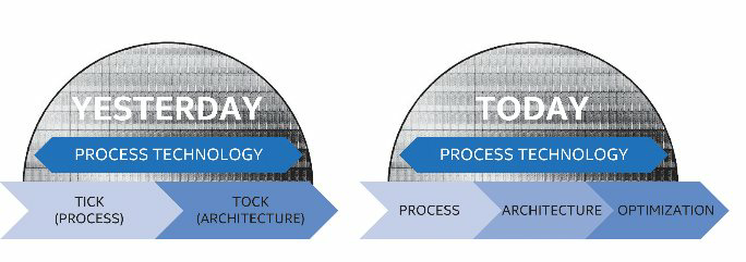
Intel refuses tick-to-talk
Now the processors will do the process-architecture-optimization cycle.
As a public company with more than $ 10 million in assets whose shares are owned by more than 500 shareholders, Intel has provided the United States Securities and Exchange Commission with an annual report on the form 10-K . Of particular interest in the 150-page document is page 14, on which Intel recognizes that it is abandoning the tick-to-do strategy in favor of the new process-architecture-optimization concept.
Tick-Tock is a microprocessor development model that Intel has been using since 2007. At certain time intervals, the technology allows to reduce the size of the elements on the board, which allows to reduce power consumption and fit more transistors on a chip of the same size. If it is possible to fit more elements, then a new microarchitecture is possible: new commands are added, the logic of work improves, the number of different elements increases.
The tick-to-do strategy separates the two processes. For the "tick" transistors become smaller. Changes in the micro-architecture are there, but they are minor. “So” means the creation of a new micro-architecture, that is, large, sometimes fundamental changes in order to achieve large productivity gains.
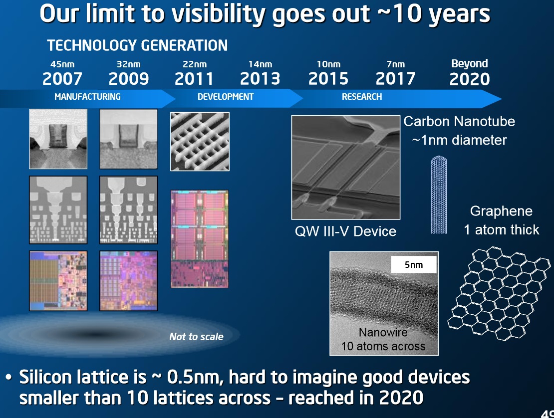
Intel has been moving with such small steps for almost 10 years. Each of them takes from one to one and a half years. But lately, reducing the process has become increasingly difficult. In the transition from 22 to 14 nanometers appeared delays of 6-9 months. At this time, it was necessary to increase the percentage of output of working chips from the plates to the level acceptable at cost. Moore's Law, which describes doubling the number of transistors on a chip every 24 months, has to be corrected.
')
In the future, the transition to 10 and then 7 and 5 nanometers is planned. Achievement of new frontiers means the possible use of lithography in the deep ultraviolet, Self-Aligned Quadruple Patterning (SAQP), the rejection of silicon in favor of III-V semiconductors, carbon nanotubes and graphene.
Slide from the presentation a year ago .
The document for the Securities and Exchange Commission affects the general course of development of Intel. The company explains that the total usage time of products on the current process technology of 14 nanometers and a future of 10 nm will be increased. But the market rate of release of new products will be maintained. How will this be achieved? Intel provides an image that is posted in this post before kata. In it, “tick-tac” is called yesterday's technology, and the current reality is the three-step cycle “process-architecture-optimization” (PAO).
14 nanometers helped to work out the "tick" Broadwell, a follower of 22-nm Haswell. Intel's current microarchitecture is Skylake, the sixth-generation Core, “so” 14-nanometer process technology. His follower, Kaby Lake, will also be 14nm, but will provide "significant performance improvements over the sixth generation Core processor family."
Achieve 10 nanometers can be helped by the cooperation with ASML in photolithography in the deep ultraviolet, mentioned in the document, which can be applied to plates with diameters of 300 and 450 millimeters. Intel still maintains leadership: 14 nm were introduced in August 2014, Samsung and TSMC were pulled up later.
The 14-nanometer Kaby Lake is expected to be released this year. According to current plans, products on the 10-nanometer Cannonlake microarchitecture should appear in 2017. In a three-step cycle, it is easy to see obvious advantages for the end user: the same motherboard can be suitable for products of two or more generations.
Source: https://habr.com/ru/post/392041/
All Articles