3D NAND flash memory technology
Hello! As you know, modern planar NAND flash memory has almost reached its potential. Its main problem is that it becomes more difficult to reduce the size of the crystal. Experts predict that 14-15 nm technological standards will be the limit of planar flash memory, at least for the near future. And it will be replaced by the technology of "vertical" flash memory - 3D NAND.
It is very important to understand what prevents further reduction of the size of the crystal. First of all, for the development of more subtle technical processes, expensive equipment is necessary, the purchase of which may not be justified from an economic point of view. And if the acquisition of new lithographic machines is a solvable issue, then the problem of the charge flowing from one cell to another, due to which errors occur, is not so easy to solve.
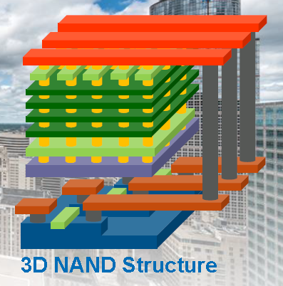
In short, the industry was in a situation where the resources of conventional, planar, flash memory were exhausted. Therefore, the idea to place the cells not only in the plane, but also in layers. Thus, the chip receives a three-dimensional structure and is capable of containing much more information per unit area than two-dimensional crystals. The technology is called 3D NAND. It is also worth noting that manufacturers use different techniques to create three-dimensional memory, so each company’s 3D NAND architecture may have its own characteristics and differences.
')

The first company to establish the production of three-dimensional flash memory called 3D V-NAND and drives based on them, was the Korean giant Samsung. Back in 2013, they announced the release of the first three-dimensional MLC-type chips with 24 layers. A year later, the TLC flash memory received a 3D implementation, the number of layers of which increased to 32.

As you know, the design of the planar flash memory is based on a floating gate transistor. Floating shutter has the ability to hold a charge for a long time. As it turned out, this is the main drawback of the design: with a decrease in technical process due to the deterioration of cells, the charge can flow from one cell to another. To solve this problem, Samsung uses 3D Charge Trap Flash technology, which translated from English means “charge trap”.

Its essence lies in the fact that the charge is now placed not in the floating gate, but in the isolated area of the cell of non-conductive material, in this case - silicon nitride (SiN). This reduces the likelihood of "leakage" of the charge and increases the reliability of the cells.
In addition, the use of CTF technology made it possible to make memory chips more economical. According to Samsung, the savings can reach 40% compared to planar memory.

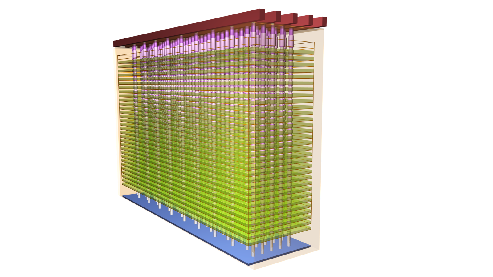
A 3D V-NAND 3D cell is a cylinder, the outer layer of which is the control gate and the inner layer is the insulator. The cells are located one above the other and form a stack, inside which a cylindrical channel of polycrystalline silicon, common to all cells, passes. The number of cells in the stack is equivalent to the number of layers of flash memory.

3D V-NAND memory also boasts a higher speed. This was achieved by simplifying the algorithm for writing to the cell - now instead of three operations, only one is performed. Simplification of the algorithm was made possible due to less interference between cells. In the case of planar memory, due to possible interference between neighboring cells, additional analysis was required before recording. Vertical memory is free of this problem, and recording is done in one step.

Well, a few words about reliability. 3D V-NAND memory is much less subject to wear due to the fact that high voltage is not required to write information to the cell. Recall that in order to place the data in a planar memory cell, a voltage of about 20 V is applied. For three-dimensional memory, this figure is lower. Reliability was positively affected by the fact that the production of three-dimensional flash memory does not require thin technological standards. For example, the third generation of 48-layer 3D V-NAND memory is produced using a well-tuned 40 nm process technology.

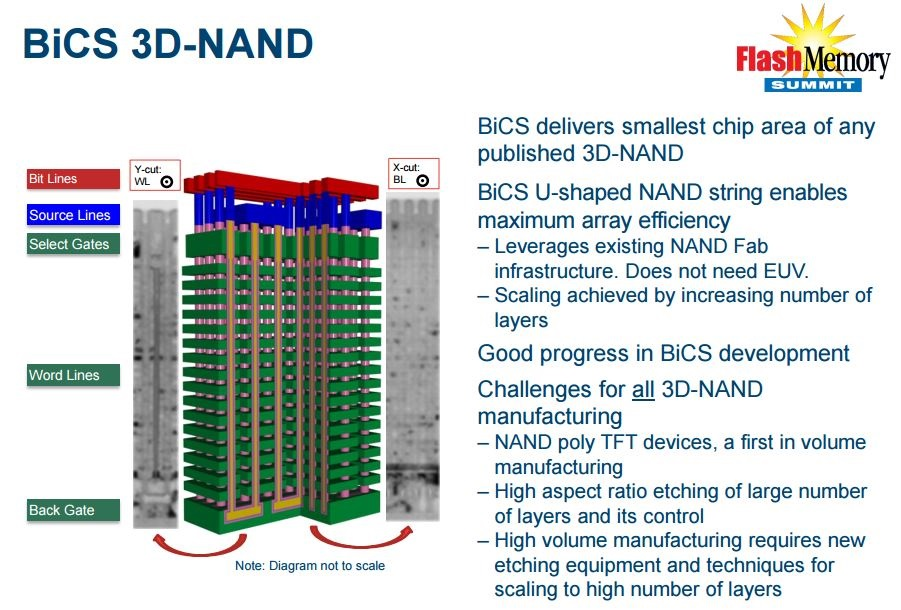
While Samsung was producing three-dimensional flash memory chips at a loss (which, by the way, was officially confirmed by a Korean company), other flash memory manufacturers developed competing technologies. For example, Toshiba and SanDisk have joined together in an alliance for the release of three-dimensional BiCS 3D NAND flash memory (Bit Cost Scalable).

Work on the technology began back in 2007 with Toshiba alone, and the first samples of the three-dimensional BiCS flash memory were demonstrated in 2009. Since then, the development of technology has not been forced. In addition, the Toshiba / SanDisk alliance made it clear that they are not going to put three-dimensional flash memory into mass production until it is economically profitable.
The main difference between Toshiba 3D flash memory and planar, as in the case of Samsung 3D V-NAND, is the use of CTF technology instead of the classic transistors with a floating gate. Silicon nitride (SiN) also serves as the material for the isolated region. The principle of the technology in BiCS 3D NAND remains the same: the information is not placed in the floating gate, as before, but in an isolated area.

What distinguishes BiCS 3D NAND from 3D V-NAND technology is the use of U-shaped lines (lines). This means that the cells are not grouped in a row, but in a U-shaped sequence. According to Toshiba, this approach allows us to achieve maximum reliability and speed. This became possible due to the fact that in a U-shaped design, the switching transistor and the source line are located in the upper part of the sequence (and not in the lower part, as in the case of a “row” design) and are not exposed to high-temperature influence, as a result of which the number of errors in reading and writing decreases .
Also among the advantages of U-shaped design, Toshiba considers the fact that this design does not require the use of photolithography in the deep ultraviolet. Therefore, for the manufacture of three-dimensional flash memory company can use existing production capacity.
It is also interesting that Toshiba will apply thin-film transistor (TFT) technology for the first time in the production of BiCS 3D NAND.

As for the technical characteristics of BiCS chips, these will be 48-layer TLC-type memory crystals. Their density will be 256 Gbps. In the production will be used debugged 30-40 nm process. In general, the characteristics of the first mass chips BiCS 3D NAND will be very similar to the third generation of crystals Samsung 3D V-NAND.
The Micron / Intel Alliance is also developing its own three-dimensional flash memory. Many experts predicted that all 3D NAND projects would use CFT technology, but Micron and Intel surprised everyone and went the other way. The basis of their three-dimensional flash memory cells are floating gate. In Micron argue that it is this architecture allows you to more safely store the charge in the cell.

In addition, CMOS Under the Array technology is used in the production of 3D NAND. Its meaning is that all control logic is not located next to an array of memory, as in 2D NAND, but under it. This design allows you to free up to 20% of the chip area and place the memory cells in this place.
Micron promises to start mass production of three-dimensional flash memory chips this year. These will be 32-layer crystals with a density of 256 Gbps (MLC) and 384 Gbps (TLC).

Not much is known about the architecture of the SK Hynix three-dimensional flash memory. Initially, the South Korean company planned to use floating-gate cells, but in the end the choice fell on CTF technology. This year, SK Hynix promises to finally start mass production of 3D NAND. These will be 48-layer TLC chips with a capacity of 256 Gbps.

As for the company OCZ, the output of SSD-drives based on three-dimensional flash memory BiCS, of course, included in our immediate plans. The release date of the new devices will depend on Toshiba, which promises to set up the supply of BiCS 3D NAND chips in the second half of this year.
It is very important to understand what prevents further reduction of the size of the crystal. First of all, for the development of more subtle technical processes, expensive equipment is necessary, the purchase of which may not be justified from an economic point of view. And if the acquisition of new lithographic machines is a solvable issue, then the problem of the charge flowing from one cell to another, due to which errors occur, is not so easy to solve.
In short, the industry was in a situation where the resources of conventional, planar, flash memory were exhausted. Therefore, the idea to place the cells not only in the plane, but also in layers. Thus, the chip receives a three-dimensional structure and is capable of containing much more information per unit area than two-dimensional crystals. The technology is called 3D NAND. It is also worth noting that manufacturers use different techniques to create three-dimensional memory, so each company’s 3D NAND architecture may have its own characteristics and differences.
')
The first company to establish the production of three-dimensional flash memory called 3D V-NAND and drives based on them, was the Korean giant Samsung. Back in 2013, they announced the release of the first three-dimensional MLC-type chips with 24 layers. A year later, the TLC flash memory received a 3D implementation, the number of layers of which increased to 32.
As you know, the design of the planar flash memory is based on a floating gate transistor. Floating shutter has the ability to hold a charge for a long time. As it turned out, this is the main drawback of the design: with a decrease in technical process due to the deterioration of cells, the charge can flow from one cell to another. To solve this problem, Samsung uses 3D Charge Trap Flash technology, which translated from English means “charge trap”.
Its essence lies in the fact that the charge is now placed not in the floating gate, but in the isolated area of the cell of non-conductive material, in this case - silicon nitride (SiN). This reduces the likelihood of "leakage" of the charge and increases the reliability of the cells.
In addition, the use of CTF technology made it possible to make memory chips more economical. According to Samsung, the savings can reach 40% compared to planar memory.
A 3D V-NAND 3D cell is a cylinder, the outer layer of which is the control gate and the inner layer is the insulator. The cells are located one above the other and form a stack, inside which a cylindrical channel of polycrystalline silicon, common to all cells, passes. The number of cells in the stack is equivalent to the number of layers of flash memory.
3D V-NAND memory also boasts a higher speed. This was achieved by simplifying the algorithm for writing to the cell - now instead of three operations, only one is performed. Simplification of the algorithm was made possible due to less interference between cells. In the case of planar memory, due to possible interference between neighboring cells, additional analysis was required before recording. Vertical memory is free of this problem, and recording is done in one step.
Well, a few words about reliability. 3D V-NAND memory is much less subject to wear due to the fact that high voltage is not required to write information to the cell. Recall that in order to place the data in a planar memory cell, a voltage of about 20 V is applied. For three-dimensional memory, this figure is lower. Reliability was positively affected by the fact that the production of three-dimensional flash memory does not require thin technological standards. For example, the third generation of 48-layer 3D V-NAND memory is produced using a well-tuned 40 nm process technology.
While Samsung was producing three-dimensional flash memory chips at a loss (which, by the way, was officially confirmed by a Korean company), other flash memory manufacturers developed competing technologies. For example, Toshiba and SanDisk have joined together in an alliance for the release of three-dimensional BiCS 3D NAND flash memory (Bit Cost Scalable).
Work on the technology began back in 2007 with Toshiba alone, and the first samples of the three-dimensional BiCS flash memory were demonstrated in 2009. Since then, the development of technology has not been forced. In addition, the Toshiba / SanDisk alliance made it clear that they are not going to put three-dimensional flash memory into mass production until it is economically profitable.
The main difference between Toshiba 3D flash memory and planar, as in the case of Samsung 3D V-NAND, is the use of CTF technology instead of the classic transistors with a floating gate. Silicon nitride (SiN) also serves as the material for the isolated region. The principle of the technology in BiCS 3D NAND remains the same: the information is not placed in the floating gate, as before, but in an isolated area.
What distinguishes BiCS 3D NAND from 3D V-NAND technology is the use of U-shaped lines (lines). This means that the cells are not grouped in a row, but in a U-shaped sequence. According to Toshiba, this approach allows us to achieve maximum reliability and speed. This became possible due to the fact that in a U-shaped design, the switching transistor and the source line are located in the upper part of the sequence (and not in the lower part, as in the case of a “row” design) and are not exposed to high-temperature influence, as a result of which the number of errors in reading and writing decreases .
Also among the advantages of U-shaped design, Toshiba considers the fact that this design does not require the use of photolithography in the deep ultraviolet. Therefore, for the manufacture of three-dimensional flash memory company can use existing production capacity.
It is also interesting that Toshiba will apply thin-film transistor (TFT) technology for the first time in the production of BiCS 3D NAND.
As for the technical characteristics of BiCS chips, these will be 48-layer TLC-type memory crystals. Their density will be 256 Gbps. In the production will be used debugged 30-40 nm process. In general, the characteristics of the first mass chips BiCS 3D NAND will be very similar to the third generation of crystals Samsung 3D V-NAND.
The Micron / Intel Alliance is also developing its own three-dimensional flash memory. Many experts predicted that all 3D NAND projects would use CFT technology, but Micron and Intel surprised everyone and went the other way. The basis of their three-dimensional flash memory cells are floating gate. In Micron argue that it is this architecture allows you to more safely store the charge in the cell.
In addition, CMOS Under the Array technology is used in the production of 3D NAND. Its meaning is that all control logic is not located next to an array of memory, as in 2D NAND, but under it. This design allows you to free up to 20% of the chip area and place the memory cells in this place.
Micron promises to start mass production of three-dimensional flash memory chips this year. These will be 32-layer crystals with a density of 256 Gbps (MLC) and 384 Gbps (TLC).
Not much is known about the architecture of the SK Hynix three-dimensional flash memory. Initially, the South Korean company planned to use floating-gate cells, but in the end the choice fell on CTF technology. This year, SK Hynix promises to finally start mass production of 3D NAND. These will be 48-layer TLC chips with a capacity of 256 Gbps.
As for the company OCZ, the output of SSD-drives based on three-dimensional flash memory BiCS, of course, included in our immediate plans. The release date of the new devices will depend on Toshiba, which promises to set up the supply of BiCS 3D NAND chips in the second half of this year.
Source: https://habr.com/ru/post/391899/
All Articles