Silicon electronics underwater stones. Problems and solutions
Welcome our dear readers to the pages of the blog iCover ! It is very likely that the monopoly of silicon chips is unlikely to be challenged in the near future. Being the second most common element after oxygen on Earth, today it is considered as an integral component of our earthly civilization. At the same time, further miniaturization of silicon transistors, as the basis of existing computing devices, is associated with a number of technological problems, which makes scientists look for an alternative to this seemingly irreplaceable material. About the directions in which the search is conducted and how successful the steps taken are described in our article.
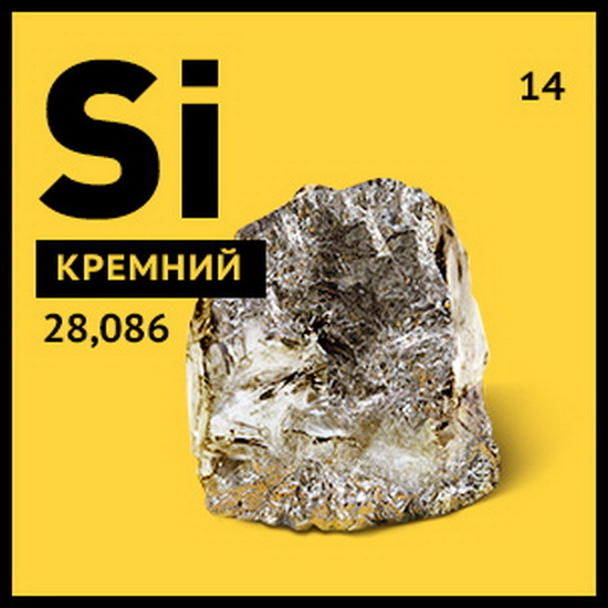
Silicon electronics has completely changed our world, determining the possibility of creating a single information space. Quartz and river sand, silicon (Si), present on Earth in colossal quantities and related in the late 40s of the last century to useless and capricious materials, gave us the opportunity to create electronic devices and information technologies, turning into that engine, without which our civilization in its present form could never exist.
The revolutionary changes that were implemented in the fields of information and computing systems and literally took place during the life of a single generation of mankind became possible due to the continuous miniaturization of the transistor - the key "workhorse" of solid-state electronics, which replaced the electronic vacuum tubes and mechanical relay switch. Such switches have found application in the scheme of the first binary electromechanical computer Z1, created in 1938 by Konrad Zuse.
')
Let's try to ask a question: how long will the miniaturization of transistor sizes, accompanied by an increase in processor performance, be technologically and economically justified? Reducing the size of transistors made it possible to increase their number on a single chip to 100,000 (1.5 micron technology) in 1982, to 100,000,000 (90 nm technology) by 2003, and to almost 10,000,000,000 today. The processor clock speeds grew steadily based on the number of operations per second. Only at the stage from 1982 to 2003, the increase was: from 10 MHz in 1982 to 4 GHz in 2003, after which this value practically did not increase. Why?
The reason for the seeming logical inconsistency lies in the fundamental principle of functioning of modern processors, which implies encoding binary values in the form of electron charge on capacitor plates (the energy equivalent of a bit is equal to = CV² / 2, where C is the capacitance and V is the voltage on its plates) . That is, when performing any manipulations with the bits, the computing device will need energy sufficient to distinguish the value of the bit from the thermal noise. At the same time, in all information processing systems that exist today, any changes in the state of a bit are accompanied by the “release” of a certain amount of thermal energy. With an increase in the clock frequency, the frequency of the release of portions of energy also increases, while maintaining the size of the chip.
Of course, the development of technology allows to reduce the size of capacitors and useful voltage, but this process is not able to compensate for the inevitable increase in power density. This, not very rational approach, justified itself until the problem associated with the heat sink required taking drastic measures.
In order to visualize the scale of the problem, recall that the 8086 microprocessor, produced in 1978 using three micron technology, enabled 29,000 transistors, and, operating at 4.77 MHz, did not require a radiator, since the amount of heat dissipated did not exceed 1.5. watt. The Pentium 4 Prescott processor, released in 2004 using a 90 nm process technology, operating at 3 GHz, used the capabilities of 125 million transistors and produced 100 watts of thermal energy. And here the developers are very close to the limit of power that can be taken using the air cooling scheme. It is in this connection that the laptop lying on our knees burns the legs and the desktop becomes part of the heating system. At the level of a modern supercomputer that consumes about 5 megawatts of power (equivalent to 1,000 four-burner electric cookers operating simultaneously at full power), a specially cooled room will be needed. A Google data center, which is being built in cold Norway, will consume 200 megawatts and be cooled by water from the nearest fjord.

Illustration of the increase in the density of power dissipated on a chip, according to the data for the period from 1970 to 2012 (University of Notre Dame, USA)
Here it is appropriate to quote the International Technology Roadmap for Semiconductors (“International Road Map for Semiconductor Technologies”): “ from packaged chips remains almost flat (ITRS 2013) ”. What does it mean: power distribution management has become a problem for most applications, due to the fact that doubling the number of transistors is not accompanied by an equivalent increase in effective heat dissipation from the chip, remaining almost at the same level.
In other words, the density of air-cooled transistors on a chip today is such that their simultaneous use will lead to the melting of the chip. This explains the need to use dark silicon modes, when a certain spatial area of the chip passively “falls asleep” for a time without passing current through itself and without generating heat. It is also important to take into account that further miniaturization of transistors to less than 10 nm (about 20 silicon atoms) exacerbates the problem of heat dissipation due to leakage problems resulting from quantum mechanical tunneling (so-called “passive” leakage).
Another problem is economic feasibility. Single transistors of such sizes are not a problem to be manufactured using electronic lithography technology. When it comes to mass production, which implies serious costs at each stage of the technological cycle without special prospects for reducing the cost of the production process, the justification for investing in such production is in doubt.
It should be noted here that today technologies are presented that open up the possibility for development in a horizontal direction, without the need to reduce the size of devices. This principle is used in circuits with multi-core parallel processors that use several chips on a single chip. Another example of a temporary way out of the impasse is the actively developing today system on a chip concept, which involves the manufacture of specialized processors to perform specific tasks. At the same time, improvisation with architecture in this case can hardly be called a fundamental solution, since the alternative to “bricks” (silicon field effect transistors) is not supposed.
Is there any reason to talk about the technological limit? It looks like yes. And this is confirmed by the active search for alternative solutions.
One of the ways is to search for a solution within the framework of standard binary digital logic, which allows to improve the parameters of modern silicon field-effect transistors and minimize the useless passive power dissipation, which is released due to leaks. Certain hopes on this path are associated with tunnel field-effect transistors (TFETs), based on the principle of quantum mechanical tunneling. An alternative solution is the use of nanoelectromechanical relays, ideally free of leaks (a kind of Konrad Zuze’s idea of a kind, in a nanoscale interpretation).
One of the contenders for the replacement of silicon being considered today is graphene. The properties of a semiconductor required for the implementation of the function of a transistor, graphene today demonstrates in the form of “nanocovers”, to mass production of unsuitable, therefore, at the current stage of technology development, silicon cannot be considered a serious competitor.
Does not meet the expectations laid so far, and so on. “Spintronics” is the principle according to which it is proposed to consider not the electron charge, but its spin (internal magnetic moment) as the equivalent of a binary variable. Being extremely costly to implement, such technology does not demonstrate any fundamental advantages in comparison with silicon solutions at this stage of its implementation.
Of course, one of the priority and most promising areas in the search for alternatives for the past 15 years seems to be a quantum computer and everything connected with it. The practical implementation of this solution faces several problems at once. The first is to manufacture a processor with the number of qubits sufficient to achieve the goals set so far is problematic, and the prospects are rather vague. On the other hand, it was not so easy to determine the range of tasks that quantum computers could solve better than existing computers. Except for the factorization of numbers and a number of other specific problems, the advantages of quantum computers in solving everyday problems are not obvious. At the same time, promising quantum computers are of the greatest interest when using quantum systems in calculations.
Are alternative solutions considered? Yes, and for this it is worth asking: Is it possible to minimize the energy release of a bit, accompanied by heat generation?

An illustration of theoretically attainable values of the power dissipation on the chip, depending on the microprocessor clock frequency for cases of ordinary and reversible logic. (University of Notre Dame, USA)
Dependencies reflected in the graph are not the only possible ones. An example is the so-called. “Adiabatic reversible logic” (ARL), based on the Landauer principle, following which the transformation of bit energy into heat is inevitable only in the case of erasing information. Accordingly, if erasure is replaced by a recirculation process, in which most of the energy of the bits is returned to the power source, then significant losses can be avoided.
As studies have confirmed, in the ARL mode, the chip can be made to work so that the amount of heat released is an order of magnitude smaller than that emitted in chips operating on standard irreversible logic. Of course, to compensate for the realizable advantage of the architecture within the chip falls at the expense of auxiliary systems that are exclusively involved in the distribution of energy resources. The role of a key element of such a system can be performed by microelectromechanical resonators used as local "distributors" of energy, working both for energy output to the consumer (transistor circuit) and for receiving energy from these devices in the opposite direction. This energy can be reused (recycled). This also increases the amount of operations that the device can perform per unit of time. As an example of the advantages of such a solution, you can bring a smartphone that will be sufficient to charge once a year or increase the computing power of the laptop tens or even hundreds of times within the same energy budget.
At the same time, although the use of ARL seems to be quite a promising solution that allows the use of already existing technologies, it’s obviously premature to speak about a fundamental breakthrough, since it is intended to use all the same transistors, with their inherent drawbacks, which manifest with a decrease in their size ( for example, ARL does not demonstrate advantages in solving the key problem of passive quantum mechanical leakage).
Is it possible to do without transistors in principle? Let's try to consider an option using the concept of so-called. QCA (quantum dot cellular automata = cellular automaton at quantum dots).
Cellular machine called computing device, which consists of a set of homogeneous "cells", very similar to the cubes of the children's designer "Lego", from which it is possible to assemble quite complex devices. Each such cell at each fixed point in time is in one of two states. A change in the state of a cell over time can be logically linked to its previous state or the states of its neighbors (in the “neighborhoods” of the cell). In 1993, Wolfgang Porod and Craig Lent from the University of Notre Dame (USA) proposed a physical prototype of such an automaton, which used the concept of electrostatic coupled quantum dots.

An illustration of two states of a QCA cell and a full binary adder assembled from such cells. Red circles - quantum dots filled with electrons. These electrons are capable of tunneling between white circles - quantum dots. Due to the Coulomb repulsion, electrons are located in one of two energy-equivalent diagonal states that encode binary zero and one. (University of Notre Dame, USA)
The minimum cell (“cell”) in the QCA architecture is composed of four quantum dots that are located at the corners of the square. There are two electrons in each cell on four points. Coulomb repulsion determines their position in mutually opposite corners of the square, and, as a result, two “diagonal” locations of electrons in this interpretation will correspond to two states with equal energy, interpreting a one or zero binary code.
How it works. (University of Notre Dame, USA)
QCA architectures are based on simple rules of interaction between cells, localized on the surface of the chip, and implementing both the idea of a cellular automaton and quantum mechanics. This architecture allows you to create nanodevices that combine high computing power with extremely low power consumption. It is very important that, on the basis of QCA, it is possible to create not only productive energy efficient processors with traditional deterministic binary logic, but also use similar architectural solutions when creating quantum computers.

Illustration of a single-electron transistor with metal electrodes and oxide tunnel junctions with an area of about 4000 square meters. nm. (University of Notre Dame, USA)
As a reader for a cellular automaton QCA can be used so-called. A “single-electron” transistor is a nanoelectronic device that allows you to track the moment of switching of one electron in a cell. The current prototype of such a device in which metal “quantum dots” were used at low temperatures (~ 100 mK) was first demonstrated back in 1997. The role of the battery for such a processor can perform a multi-phase clock oscillator on the chip, made on the basis of the resonator and capable of both delivering and absorbing energy. By the way, a one-electron logic circuit (“one-electron parametron”) with a clock generator, which has found application in the QCA architecture, was proposed by A. Korotkov and K. Likharev.
One of the cornerstones is that the characteristic energy scale of the barrier separating binary 0 and 1 in electronic QCAs depends on the parameter, which, in turn, is determined by the electrical capacity of the system, C: E = e² / C. Accordingly, in order for such a QCA scheme to work at room temperature, the permissible dimensions of the cell should not exceed 5 nanometers. At the same time, the possibility of creating and successfully operating such a (single) cell at room temperature was first demonstrated in 2009 by a group of specialists under the leadership of Robert Wolkow. Unfortunately, the solutions obtained at the commercial level were never implemented.

Illustration of a full binary adder on nanomagnets with dimensions of 80 x 60 square meters. nm. Right MSM image, left - electron micrograph. Formed magnetic poles are displayed in bright and dark colors. (University of Notre Dame, USA)
The principles underlying the concept of QCA, allow you to create not only nanoelectronic, but also nanomagnetic processors, “Lego” cubes in which nanomagnets with two fixed magnetisation directions and less than 100 nm in size play the role. Logical nodes of this kind of devices, made of permalloy, were demonstrated back in 2006 and were able to successfully combine the functions of both memory and logic device.
In the future, the operation of such cellular automata will be ensured by minimal switching powers and the use of an adiabatic reversal scheme, which will minimize useless energy dissipation. Such automata can be assembled from specific molecules with elements of a single-bit cell inside them. ( 10¹²/²).

QCA-, (University of Notre Dame, USA)
, , , , . . .
() — -?
Hitachi () , , TOLOP (TOwards LOw Power information and communication technologies).
, , - (CMOS) , , . , .
« , , » — - (Gonzales-Zalba), .
, - .
«-» , . , , , .

, , . 20 . -. , .

- . , , 100 .
- . LC-, 350 . , «» , , . , , , .
, , -- 100 . , 1 — , , .
, — . - , .
, « , , » . « , , , , ».
ACS Nano Letters .
, , , - , . , , , .
1
2
Dear readers, we are always happy to meet and wait for you on the pages of our blog. We are ready to continue to share with you the latest news, review materials and other publications, and we will try to do everything possible so that the time spent with us will be useful for you. And, of course, do not forget to subscribe to our headings .

Our other articles and events
Silicon electronics has completely changed our world, determining the possibility of creating a single information space. Quartz and river sand, silicon (Si), present on Earth in colossal quantities and related in the late 40s of the last century to useless and capricious materials, gave us the opportunity to create electronic devices and information technologies, turning into that engine, without which our civilization in its present form could never exist.
The revolutionary changes that were implemented in the fields of information and computing systems and literally took place during the life of a single generation of mankind became possible due to the continuous miniaturization of the transistor - the key "workhorse" of solid-state electronics, which replaced the electronic vacuum tubes and mechanical relay switch. Such switches have found application in the scheme of the first binary electromechanical computer Z1, created in 1938 by Konrad Zuse.
')
Let's try to ask a question: how long will the miniaturization of transistor sizes, accompanied by an increase in processor performance, be technologically and economically justified? Reducing the size of transistors made it possible to increase their number on a single chip to 100,000 (1.5 micron technology) in 1982, to 100,000,000 (90 nm technology) by 2003, and to almost 10,000,000,000 today. The processor clock speeds grew steadily based on the number of operations per second. Only at the stage from 1982 to 2003, the increase was: from 10 MHz in 1982 to 4 GHz in 2003, after which this value practically did not increase. Why?
The reason for the seeming logical inconsistency lies in the fundamental principle of functioning of modern processors, which implies encoding binary values in the form of electron charge on capacitor plates (the energy equivalent of a bit is equal to = CV² / 2, where C is the capacitance and V is the voltage on its plates) . That is, when performing any manipulations with the bits, the computing device will need energy sufficient to distinguish the value of the bit from the thermal noise. At the same time, in all information processing systems that exist today, any changes in the state of a bit are accompanied by the “release” of a certain amount of thermal energy. With an increase in the clock frequency, the frequency of the release of portions of energy also increases, while maintaining the size of the chip.
Of course, the development of technology allows to reduce the size of capacitors and useful voltage, but this process is not able to compensate for the inevitable increase in power density. This, not very rational approach, justified itself until the problem associated with the heat sink required taking drastic measures.
In order to visualize the scale of the problem, recall that the 8086 microprocessor, produced in 1978 using three micron technology, enabled 29,000 transistors, and, operating at 4.77 MHz, did not require a radiator, since the amount of heat dissipated did not exceed 1.5. watt. The Pentium 4 Prescott processor, released in 2004 using a 90 nm process technology, operating at 3 GHz, used the capabilities of 125 million transistors and produced 100 watts of thermal energy. And here the developers are very close to the limit of power that can be taken using the air cooling scheme. It is in this connection that the laptop lying on our knees burns the legs and the desktop becomes part of the heating system. At the level of a modern supercomputer that consumes about 5 megawatts of power (equivalent to 1,000 four-burner electric cookers operating simultaneously at full power), a specially cooled room will be needed. A Google data center, which is being built in cold Norway, will consume 200 megawatts and be cooled by water from the nearest fjord.
Illustration of the increase in the density of power dissipated on a chip, according to the data for the period from 1970 to 2012 (University of Notre Dame, USA)
Here it is appropriate to quote the International Technology Roadmap for Semiconductors (“International Road Map for Semiconductor Technologies”): “ from packaged chips remains almost flat (ITRS 2013) ”. What does it mean: power distribution management has become a problem for most applications, due to the fact that doubling the number of transistors is not accompanied by an equivalent increase in effective heat dissipation from the chip, remaining almost at the same level.
In other words, the density of air-cooled transistors on a chip today is such that their simultaneous use will lead to the melting of the chip. This explains the need to use dark silicon modes, when a certain spatial area of the chip passively “falls asleep” for a time without passing current through itself and without generating heat. It is also important to take into account that further miniaturization of transistors to less than 10 nm (about 20 silicon atoms) exacerbates the problem of heat dissipation due to leakage problems resulting from quantum mechanical tunneling (so-called “passive” leakage).
Another problem is economic feasibility. Single transistors of such sizes are not a problem to be manufactured using electronic lithography technology. When it comes to mass production, which implies serious costs at each stage of the technological cycle without special prospects for reducing the cost of the production process, the justification for investing in such production is in doubt.
It should be noted here that today technologies are presented that open up the possibility for development in a horizontal direction, without the need to reduce the size of devices. This principle is used in circuits with multi-core parallel processors that use several chips on a single chip. Another example of a temporary way out of the impasse is the actively developing today system on a chip concept, which involves the manufacture of specialized processors to perform specific tasks. At the same time, improvisation with architecture in this case can hardly be called a fundamental solution, since the alternative to “bricks” (silicon field effect transistors) is not supposed.
Is there any reason to talk about the technological limit? It looks like yes. And this is confirmed by the active search for alternative solutions.
One of the ways is to search for a solution within the framework of standard binary digital logic, which allows to improve the parameters of modern silicon field-effect transistors and minimize the useless passive power dissipation, which is released due to leaks. Certain hopes on this path are associated with tunnel field-effect transistors (TFETs), based on the principle of quantum mechanical tunneling. An alternative solution is the use of nanoelectromechanical relays, ideally free of leaks (a kind of Konrad Zuze’s idea of a kind, in a nanoscale interpretation).
One of the contenders for the replacement of silicon being considered today is graphene. The properties of a semiconductor required for the implementation of the function of a transistor, graphene today demonstrates in the form of “nanocovers”, to mass production of unsuitable, therefore, at the current stage of technology development, silicon cannot be considered a serious competitor.
Does not meet the expectations laid so far, and so on. “Spintronics” is the principle according to which it is proposed to consider not the electron charge, but its spin (internal magnetic moment) as the equivalent of a binary variable. Being extremely costly to implement, such technology does not demonstrate any fundamental advantages in comparison with silicon solutions at this stage of its implementation.
Of course, one of the priority and most promising areas in the search for alternatives for the past 15 years seems to be a quantum computer and everything connected with it. The practical implementation of this solution faces several problems at once. The first is to manufacture a processor with the number of qubits sufficient to achieve the goals set so far is problematic, and the prospects are rather vague. On the other hand, it was not so easy to determine the range of tasks that quantum computers could solve better than existing computers. Except for the factorization of numbers and a number of other specific problems, the advantages of quantum computers in solving everyday problems are not obvious. At the same time, promising quantum computers are of the greatest interest when using quantum systems in calculations.
Are alternative solutions considered? Yes, and for this it is worth asking: Is it possible to minimize the energy release of a bit, accompanied by heat generation?
An illustration of theoretically attainable values of the power dissipation on the chip, depending on the microprocessor clock frequency for cases of ordinary and reversible logic. (University of Notre Dame, USA)
Dependencies reflected in the graph are not the only possible ones. An example is the so-called. “Adiabatic reversible logic” (ARL), based on the Landauer principle, following which the transformation of bit energy into heat is inevitable only in the case of erasing information. Accordingly, if erasure is replaced by a recirculation process, in which most of the energy of the bits is returned to the power source, then significant losses can be avoided.
As studies have confirmed, in the ARL mode, the chip can be made to work so that the amount of heat released is an order of magnitude smaller than that emitted in chips operating on standard irreversible logic. Of course, to compensate for the realizable advantage of the architecture within the chip falls at the expense of auxiliary systems that are exclusively involved in the distribution of energy resources. The role of a key element of such a system can be performed by microelectromechanical resonators used as local "distributors" of energy, working both for energy output to the consumer (transistor circuit) and for receiving energy from these devices in the opposite direction. This energy can be reused (recycled). This also increases the amount of operations that the device can perform per unit of time. As an example of the advantages of such a solution, you can bring a smartphone that will be sufficient to charge once a year or increase the computing power of the laptop tens or even hundreds of times within the same energy budget.
At the same time, although the use of ARL seems to be quite a promising solution that allows the use of already existing technologies, it’s obviously premature to speak about a fundamental breakthrough, since it is intended to use all the same transistors, with their inherent drawbacks, which manifest with a decrease in their size ( for example, ARL does not demonstrate advantages in solving the key problem of passive quantum mechanical leakage).
Is it possible to do without transistors in principle? Let's try to consider an option using the concept of so-called. QCA (quantum dot cellular automata = cellular automaton at quantum dots).
Cellular machine called computing device, which consists of a set of homogeneous "cells", very similar to the cubes of the children's designer "Lego", from which it is possible to assemble quite complex devices. Each such cell at each fixed point in time is in one of two states. A change in the state of a cell over time can be logically linked to its previous state or the states of its neighbors (in the “neighborhoods” of the cell). In 1993, Wolfgang Porod and Craig Lent from the University of Notre Dame (USA) proposed a physical prototype of such an automaton, which used the concept of electrostatic coupled quantum dots.
An illustration of two states of a QCA cell and a full binary adder assembled from such cells. Red circles - quantum dots filled with electrons. These electrons are capable of tunneling between white circles - quantum dots. Due to the Coulomb repulsion, electrons are located in one of two energy-equivalent diagonal states that encode binary zero and one. (University of Notre Dame, USA)
The minimum cell (“cell”) in the QCA architecture is composed of four quantum dots that are located at the corners of the square. There are two electrons in each cell on four points. Coulomb repulsion determines their position in mutually opposite corners of the square, and, as a result, two “diagonal” locations of electrons in this interpretation will correspond to two states with equal energy, interpreting a one or zero binary code.
How it works. (University of Notre Dame, USA)
QCA architectures are based on simple rules of interaction between cells, localized on the surface of the chip, and implementing both the idea of a cellular automaton and quantum mechanics. This architecture allows you to create nanodevices that combine high computing power with extremely low power consumption. It is very important that, on the basis of QCA, it is possible to create not only productive energy efficient processors with traditional deterministic binary logic, but also use similar architectural solutions when creating quantum computers.
Illustration of a single-electron transistor with metal electrodes and oxide tunnel junctions with an area of about 4000 square meters. nm. (University of Notre Dame, USA)
As a reader for a cellular automaton QCA can be used so-called. A “single-electron” transistor is a nanoelectronic device that allows you to track the moment of switching of one electron in a cell. The current prototype of such a device in which metal “quantum dots” were used at low temperatures (~ 100 mK) was first demonstrated back in 1997. The role of the battery for such a processor can perform a multi-phase clock oscillator on the chip, made on the basis of the resonator and capable of both delivering and absorbing energy. By the way, a one-electron logic circuit (“one-electron parametron”) with a clock generator, which has found application in the QCA architecture, was proposed by A. Korotkov and K. Likharev.
One of the cornerstones is that the characteristic energy scale of the barrier separating binary 0 and 1 in electronic QCAs depends on the parameter, which, in turn, is determined by the electrical capacity of the system, C: E = e² / C. Accordingly, in order for such a QCA scheme to work at room temperature, the permissible dimensions of the cell should not exceed 5 nanometers. At the same time, the possibility of creating and successfully operating such a (single) cell at room temperature was first demonstrated in 2009 by a group of specialists under the leadership of Robert Wolkow. Unfortunately, the solutions obtained at the commercial level were never implemented.
Illustration of a full binary adder on nanomagnets with dimensions of 80 x 60 square meters. nm. Right MSM image, left - electron micrograph. Formed magnetic poles are displayed in bright and dark colors. (University of Notre Dame, USA)
The principles underlying the concept of QCA, allow you to create not only nanoelectronic, but also nanomagnetic processors, “Lego” cubes in which nanomagnets with two fixed magnetisation directions and less than 100 nm in size play the role. Logical nodes of this kind of devices, made of permalloy, were demonstrated back in 2006 and were able to successfully combine the functions of both memory and logic device.
In the future, the operation of such cellular automata will be ensured by minimal switching powers and the use of an adiabatic reversal scheme, which will minimize useless energy dissipation. Such automata can be assembled from specific molecules with elements of a single-bit cell inside them. ( 10¹²/²).
QCA-, (University of Notre Dame, USA)
, , , , . . .
- — ?
() — -?
Hitachi () , , TOLOP (TOwards LOw Power information and communication technologies).
, , - (CMOS) , , . , .
« , , » — - (Gonzales-Zalba), .
, - .
«-» , . , , , .
, , . 20 . -. , .
- . , , 100 .
- . LC-, 350 . , «» , , . , , , .
, , -- 100 . , 1 — , , .
, — . - , .
, « , , » . « , , , , ».
ACS Nano Letters .
, , , - , . , , , .
1
2
Dear readers, we are always happy to meet and wait for you on the pages of our blog. We are ready to continue to share with you the latest news, review materials and other publications, and we will try to do everything possible so that the time spent with us will be useful for you. And, of course, do not forget to subscribe to our headings .
Our other articles and events
Source: https://habr.com/ru/post/391129/
All Articles