Development of a low-power backup power source with a sine output. Part 3. Work on the bugs
Foreword
In the series of articles " Development of low-power backup power source with a sine output " describes the process of designing and creating a RIP for the circulating pump of the heating system. In the second part of the narration, the author proposed to the
Lyrical digression
After the publication of the second part of the story, the author posted a link to a series of articles on the community easyelectronics.ru . This was done so that experienced radio amateurs would evaluate the author’s circuit solutions, point out critical errors, and suggest options for improving and simplifying the circuit.
Let's start to understand the source diagrams. As we analyze, and also taking into account user comments, we will bring the scheme to
Next will be presented the individual nodes of the scheme, which have undergone changes, and at the end a generalized electrical circuit designed in Dip Trace CAD system.
')
Power scheme
The power scheme based on 1% LDO stabilizers has not changed. Although many were in favor of replacing an LDO with 5 volts with a regular LM7805, arguing that the LMK case could dissipate more power. After all, the bus consumption of 5 volts will be about 250 - 300 mA, which in terms of power dissipation: P = (Uin-Uout) * I = (12-5) * 0.3 = 2.1 W. As for the SOT case - 223, it is simply a transcendental value.
The main current consumption on the 5 volt power bus will select a LCD display. The LCD backlight will not be constant, it will basically be turned off, so that the current consumption on this bus will be two times less. That is, we need to dissipate 1W. To do this, we select a decent polygon on the printed circuit board, as suggested in the commentary , so there should be no problems with this.
On a 3.3 volt bus, an LDO with a range on the board should work without any problems and overheating.
A comment was made regarding the output capacitances for these types of LDO NCP1117ST, that they may be critical for the stable operation of the stabilizer. Let's see the datasheet:
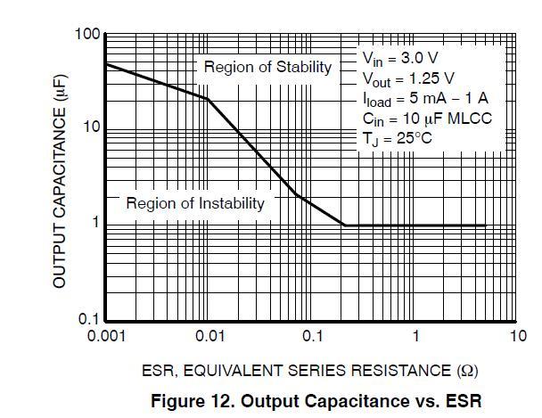
As far as I understand from this diagram, almost any capacitor, with a capacity of 47 microfarads and above, will drive the LDO into a stable mode of operation and it is not very important what kind of EPP it has. Correct if I'm wrong. With food finished, we went further.
Schottky diode
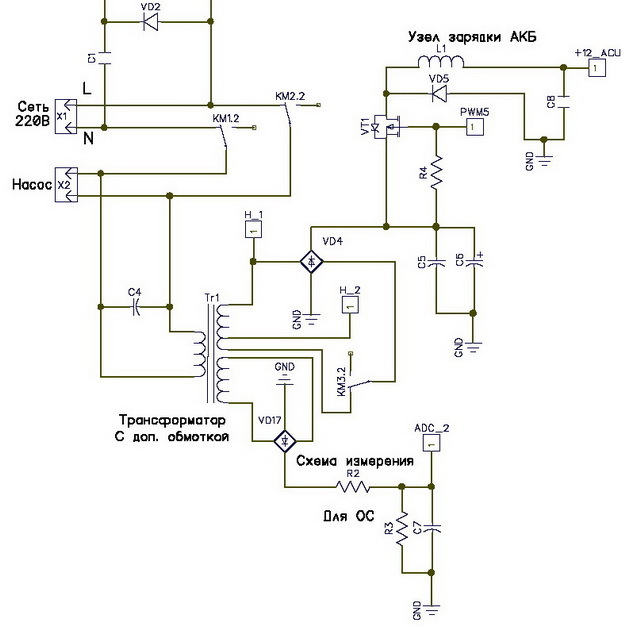
Recall the original scheme.
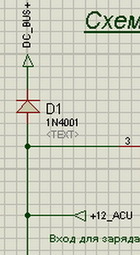
The diode decouples the battery from the bridge's power bus. As correctly noted in this comment , in it in the mode of operation from the battery will be allocated more power. 10 A Schottky diode has a direct drop on a 0.8 volt diode. At a current of 5 A, 4 W will dissipate on it. Too much. In addition, to lose 0.8 Volts do not want to. So follow the advice and put the P-channel mosfet. IRF9310 has an open channel resistance of 0.0046 Ohms. So the power dissipation will be P = I * I * R = 5 * 5 * 0.0046 = 0.115 watts. One and a half order less. The voltage drop across the transistor will be U = I * R = 5 * 0.0046 = 23 mV. Not at all noticeable. Total we get this scheme.
Manage this mosfet will MK. When working from the battery, open, when charging the battery from the network, close. Everything is logical. In addition, it is comparable in cost to the Schottky diode, so that there will be no increase in the cost of the device in this component.
Transformer
A critical error has crept into this node. Consider the original version.
When working from the battery, when the bridge is working on the transformer, when current flows from the beginning of the winding to its removal, at the end of the winding, an emf of negative polarity is generated relative to the ground of the circuit. Further, this EMF through the diode flows to the ground of the device, thereby creating a short circuit. With an emf voltage of 3-4 volts, the short circuit current will be on the order of several tens of amperes, which is bad for both the diode, the winding, and the device as a whole. That is, when short circuit on the tap in the low-voltage winding will not be able to get the required amplitude for the pump. Current protection, too, in this case will be useless. In a word, the device will not work, so it will also eat the floor of the circuit. This situation was clearly seen in several comments. For example, here and here . There are several outputs in this case.
- Wind the full independent winding to charge the battery,
- Leave this lead winding to hang in the air while running from the battery,
- Maybe something else you can think of.
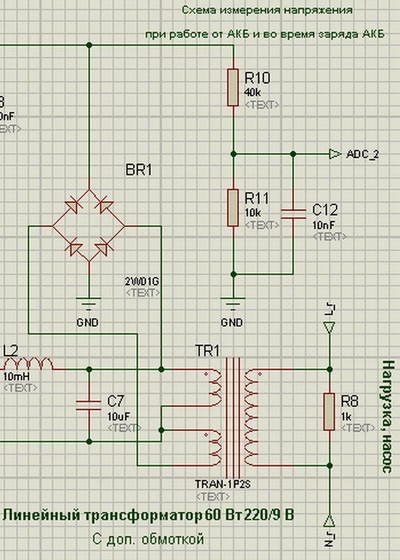
I stopped at the second option. During operation of the battery, the relay will break this winding pin from the diode rectifier charging bridge, and connect it during charging, thereby providing an increased charging voltage.
Now for the measurement circuit for feedback. She, too, will not work in such an inclusion. Since the voltage from the diode bridge passes smoothing on the high-capacity capacitors, during the operation of the battery, a constant voltage will be set at the output of the resistive divider with almost no response to changes in the voltage on the winding. So the PID control of the output voltage for this signal is not provided. For the decision, I propose, to save additional independent measuring winding. With the release of volts 5-6. Straighten the diode bridge, smooth out with a small capacitance with a time constant of 5-7 ms, and drive the already given signal to the ADC of the MK for feedback. The benefit of the power taken from such a winding will be scanty. So, the overall efficiency of the transformer is practically not affected, so the consumption from the battery will not increase much, by 10-15 mA. The wire for such a winding will need thin, and provide speed in 1-1.5 period for control.
The final scheme of this site was such.
The network detection scheme remained unchanged. The only thing that will have to be added is software debugging from the detector.
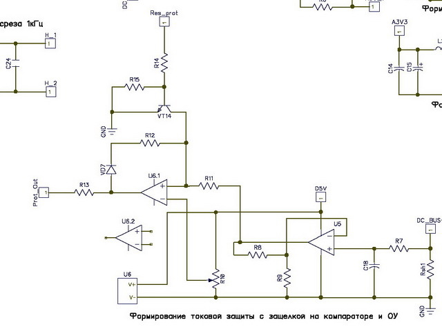
High-speed overcurrent protection on shunt
The scheme itself has not changed. The signal from the shunt is amplified on the operational amplifier, then it is turned on to the comparator. The output of the comparator when triggered becomes on the latch through the diode. The signal itself enters the MK, and is also intended to disable ALL bridge transistors. Everything would be fine, but the reset circuit of the generated comparator does not implement current protection at the moment of pressing the “RESET” button, as was correctly noted in this commentary .
I see the solution to this problem as such. Button "RESET" start on the MK. Algorithm in MK to fix the pressing and release of the button. Next, through the transistor to reset protection. And only after the arrival of the signal in the MK, that the protection is not active, start generating PWM on the bridge. Thus, if the cause of the overload has not been eliminated, then the current protection will work again, and it is not important whether the user presses the button or not. By the way, by pressing the button, during operation of the device we will turn on the LCD backlight for a few seconds. Total scheme turned out like this.
Relay control
The circuit uses 3 relays at 12 volts. Two of them have a high-resistance coil and rather weak contacts, 1 A per group. For switching high voltage 220 volts is enough with a margin, because the load power is 60 watts pump, and 20-60 watts during battery charging. That is, we fit into the floor of an amp. But the relay at number 3, already commutes 5 amperes of charging current, during a decent time. So the relay having contacts on such a current, the resistance of the coil is already 400 ohms.
We will control the relay through NPN transistors with MK. The relay will be energized only during the operation of the RIP on the load from the battery. So the time of the relay will be calculated a few hours a week, and even less. But even this fact inclines to the fact that while the relay coils are under current, to reduce the consumption of this current to a minimum.
This article is well written, how can this be achieved without resorting to too complex schemes.
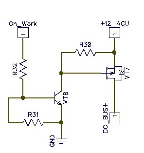
The picture shows a separate control unit coil relay.
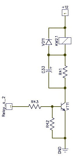
Calculate the resistors and capacitors for such a relay. Relay type: HJR4102-L-12VDC-SZ and SRD-12VDC-SL-C.
Calculate the current consumption of the relay in the usual inclusion. I = Upit / Rcat = 12/720 = 0.0167 A = 16.7 mA. This current will consume the coil. To keep the armature in the drawn state, the current can be lowered by a third. That is, I = 16.7 * (2/3) = 11 mA. Round this value to 10 mA. Now the total resistance should be. R = U / I = 12/10 * 10-3 = 1200 Ω. Of these, 720 ohms is the resistance of the coil, additional resistance comes out Rr = 1200-720 = 480 ohms. Choose from the standard row down. 470 ohms, the size of the SMD resistor will take 1206. The dissipated power of this frame size is 0.25 watts. Now let's calculate the power that will really stand out on such a resistor. P = I * I * R = 10 * 10-3 * 10 * 10-3 * 470 = 47000 * 10-6 = 0.047 W. So it doesn't even heat up the resistor. By analogy, the value of the resistor for 400 ohm coils will turn out to be 200 Ohms. Take a little smaller from the standard series - 180 Ohms. Holding current will be at 20 mA. The dissipated power of this resistor is P = 0.072 W. It also does not exceed the stated for this size in 0.25 watts.
Calculate the capacitance of capacitors, to ensure the current "stall" anchor. Let's set the time of “breaking” the armature and turning on the relay for 20 ms. The current flowing through the coil at this point should be 30 mA for the “boosted” coil. Hence, C = t * I / U = 20 * 10-3 * 30 * 10-3 / 12 = 50 * 10-6 F = 50 μF. Increase capacity by half, for greater certainty, i.e. we get 100 uF. For weaker coils, half of this capacity is enough.
Formation of impulses for H - bridge
In the second part of the story, I decided that I would use one PWM output with MK, and two outputs, commuting shoulders of the bridge. Collect all this on logic, and send the resulting signals to the key drivers.
Link to the scheme of this approach here .
In the comments, here and here , clearly showed the inconsistency of this approach, because the selected MC allows you to generate PWM, as needed, for each personal key, without any special software problems.
Lyrical digression
I am not a guru in MK programming, especially in STM32. I began to study the 32 bit MK on the core Cortex-M3, M4 just 4 months ago. So, probably, such “pens” with logic are forgivable to me. By the way, as I study, I share my impressions and knowledge in a series of video lessons. These lessons are available at this link . There are not many of them yet, but as they are studied, they will grow.
Total scheme of formation of pulses simplified. No logic chip. All four PWM channels directly from the MK go to the drivers. The input from the current protection comparator, enters the MC, on the leg, which hardware switches off the PWM on all outputs.
The final algorithm will be something like this. In MK, a sinusoidal PWM is generated at the output of CH1 and CH1N. That is, for the shoulder of the bridge, we get PWM on both keys, through dead time. This is the first half-wave, at this moment on CH2 zero, and on CH2N one, that is, the lower key of the second shoulder is open. The next half-wave will be exactly the opposite. CH2 and CH2N through dead time, generate a sinusoidal PWM, and one comes to CH1N. And so on in the cycle, more precisely, according to the DMA to "infinity". All software solutions will publish in the next article, with source codes and explanations.
Let's sum up
After all the changes in the circuitry, the
The schematics as well as the specification for the components are presented below. Specification under the spoiler.
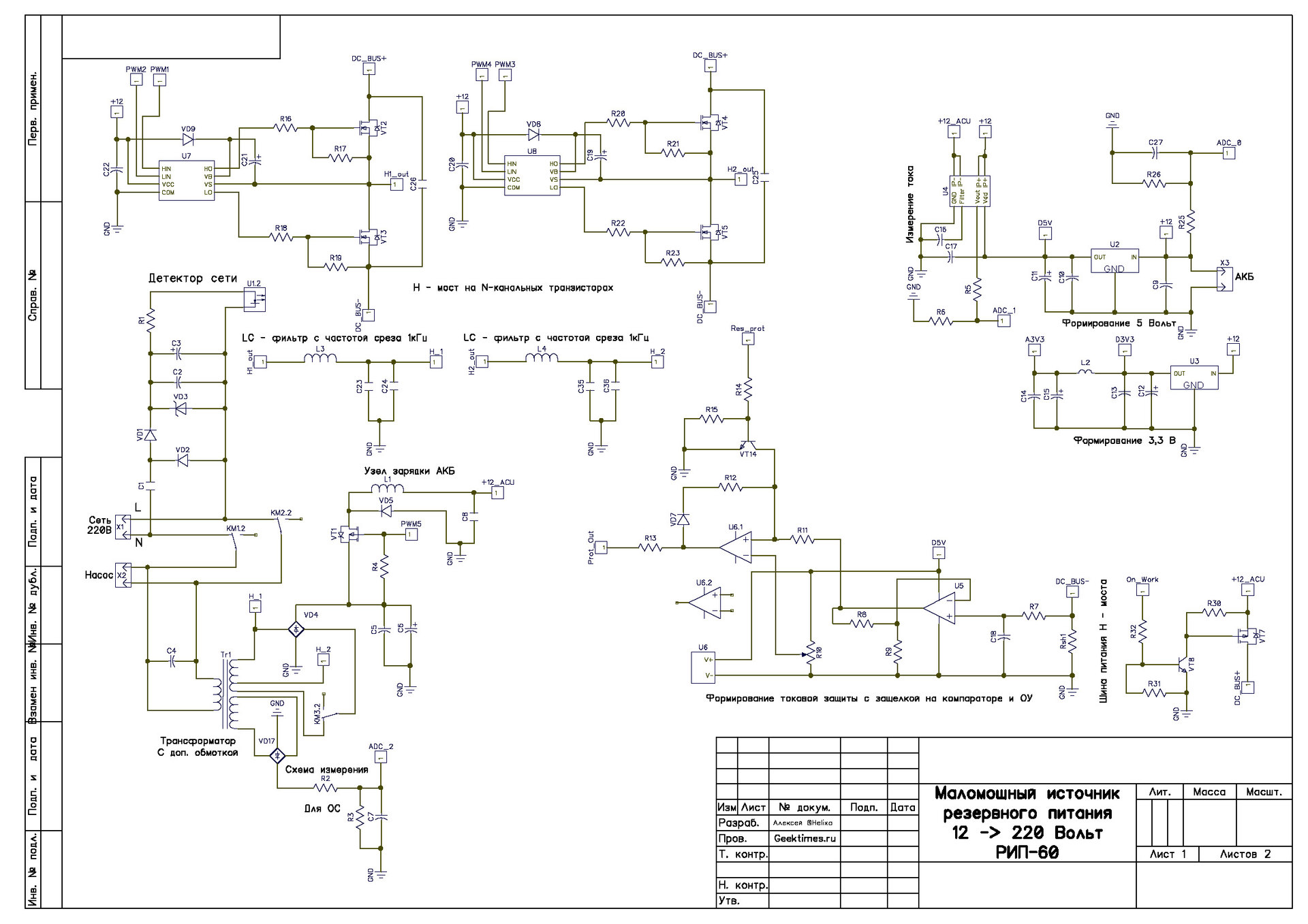
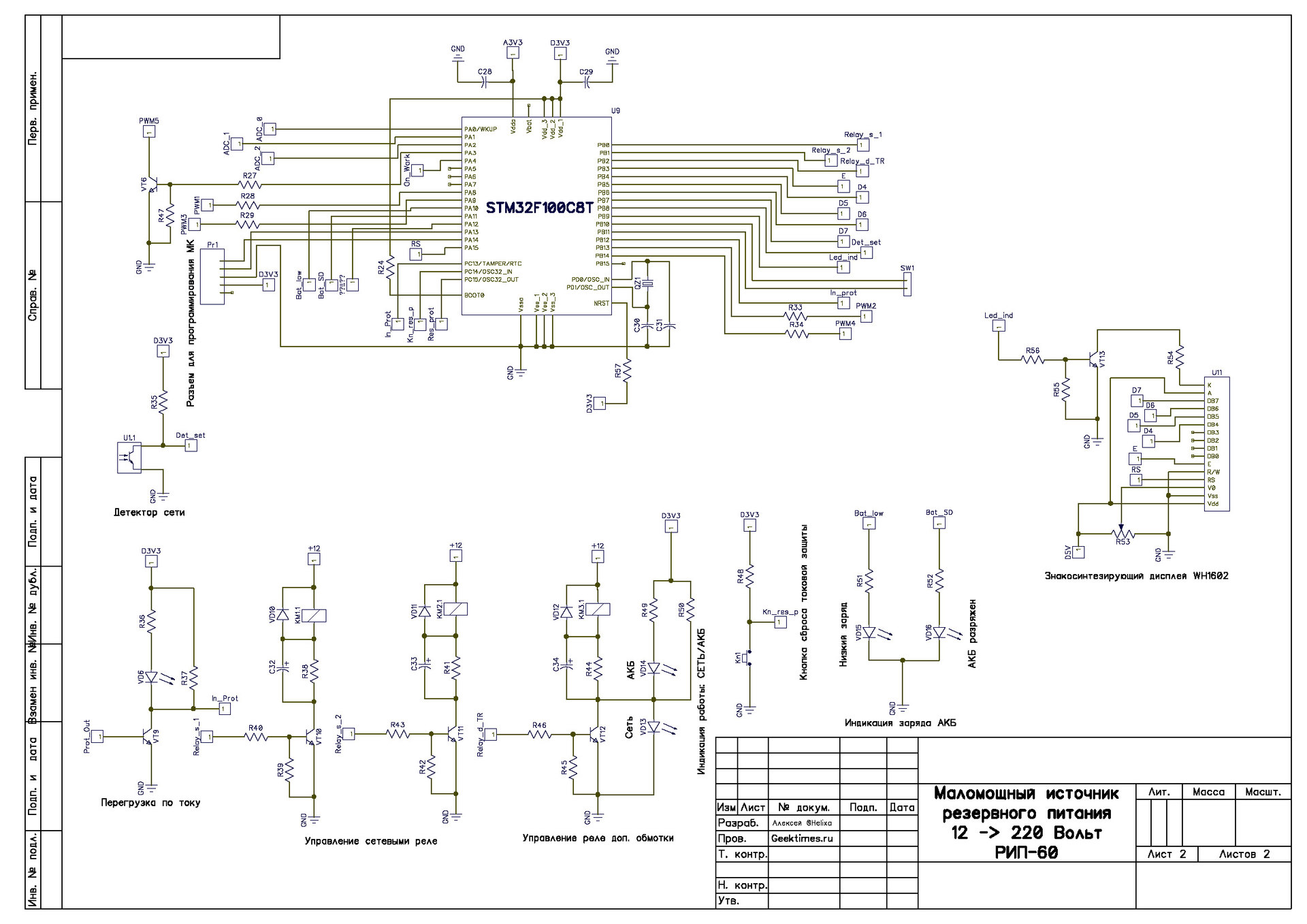
Sheet number 1. The picture is clickable
Sheet number 2. The picture is clickable
Specification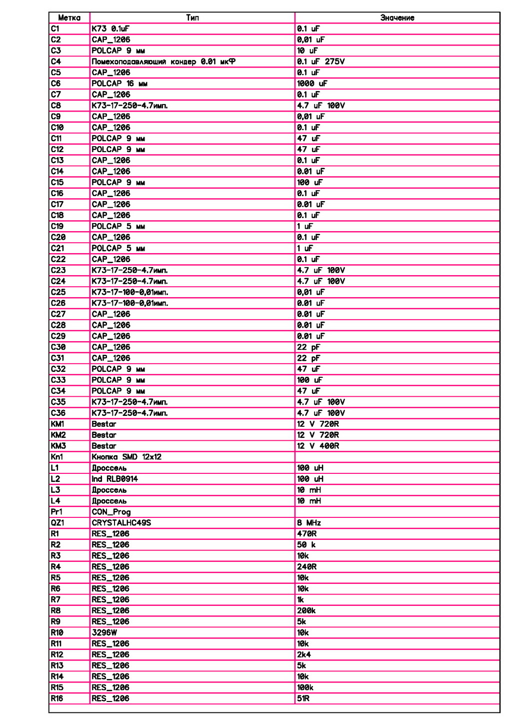
First sheet
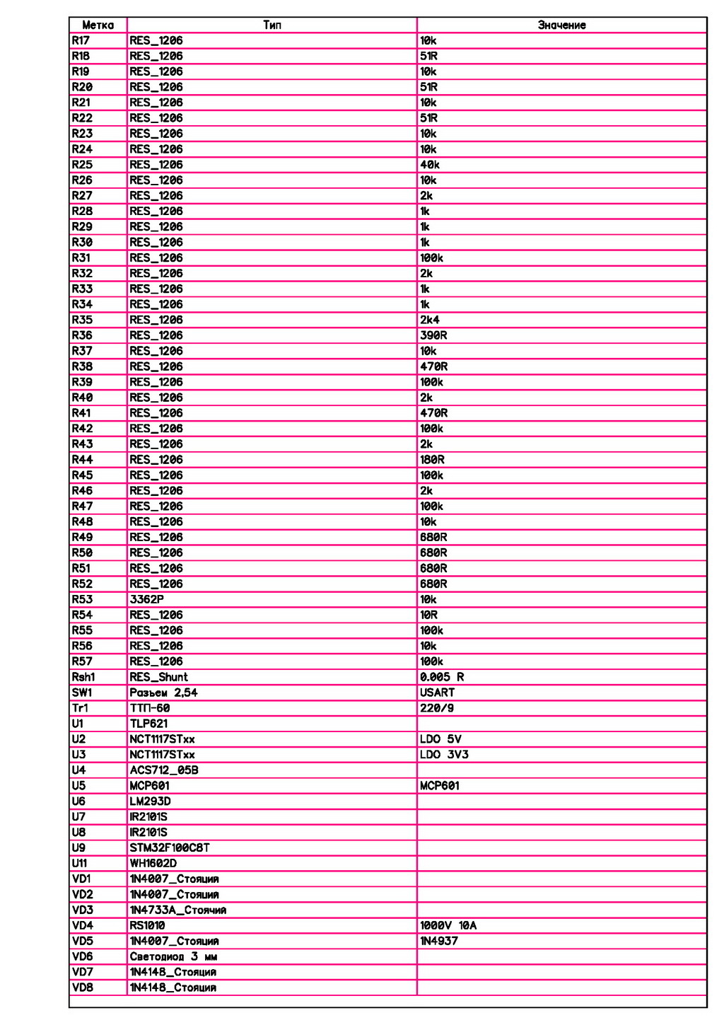
Second sheet
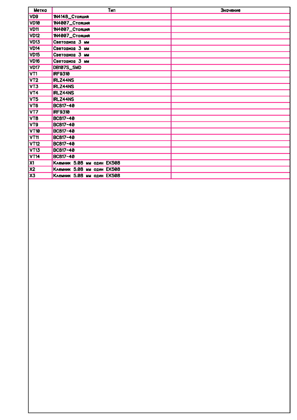
Third sheet (until the last)
First sheet
Second sheet
Third sheet (until the last)
Conclusion
After all the upgrades, changes stopped on such a scheme. Now, according to the specification, I will make an order for radio components that I do not have in stock. And as it turns out, I have about a penny resistors, capacitors, NPN - transistors and terminal blocks and nothing. So the task arose to make the purchase of radio components. Fortunately, for the manufacture of PCB method LUTa have all the necessary consumables.
The main order will be made in the online store http://chip-nn.ru/ . But a transformer, large-capacity film capacitors will have to be purchased at http://chipdip.ru. Something all in one place could not be found.
Here is the purchase statement at the moment.
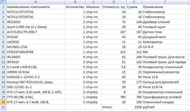
The amount is already obtained decent. To this should be added small things, rubles per 100. Fee - 100. LCD display, which I was lying around. At today's rate, it costs about 500 rubles. Then the body, some for all this stuff. So, at the cost of a radio amateur, let's get closer to the amount of 3,500 rubles.
Since weekends and holidays are close, then I will issue an order immediately after the holiday of real men.
Epilogue
I want to thank everyone who took part in the discussion and brainstorming when considering the circuit design of this device. Special human THANKS to those who found critical comments in the scheme, and also offered more correct and simple solutions of some nodes.
PS
Links to all parts of the cycle:
Source: https://habr.com/ru/post/390609/
All Articles