Backup power supply with sine output. Part 2. Development of electrical concepts
Prologue
In the last article , we considered the formulation of the problem of developing a low-power backup power source of 60 W with a sine output for the heating circulating pump. The concept of the implementation of this device was chosen. This article will discuss the development of the electrical circuit of the device, with the necessary calculations to select the ratings of the components included in the device.
Armed with
Catering
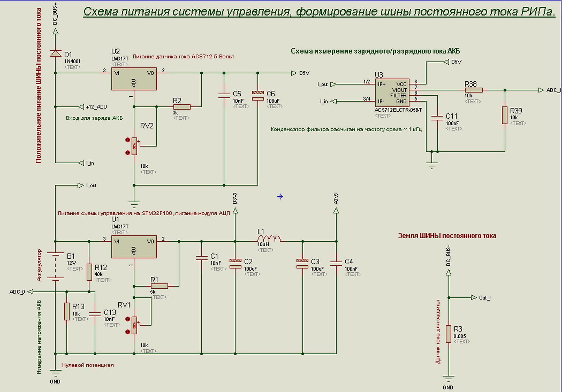
To power the circuit elements, we need three
')
Twelve volt bus - the main one. It is the power supply of the bridge, which injects current into the low-voltage winding of the linear network transformer. From it we feed the drivers of transistors included in the bridge. Commuting relays will also be powered from this bus.
The five-volt bus is needed to power the ACS712 current chip, logic chip, character LCD, etc.
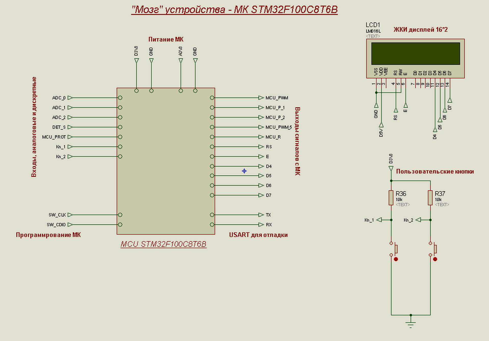
A three-volt bus will power the “brains” of the device - the MK STM32F100C8T6B.
Lyrical digression
For clarity, the pieces of the scheme were drawn in Proteuse v 7.7. Its libraries do not have all the components used, so some components are replaced by analogues. The final, complete scheme will be in the Dip Trace CAD format. With all approved components. But this is already in the next article.
This scheme was born:
The picture is clickable.
Tire shapers 5 and 3.3 Volts are organized on 1% LDO stabilizers like NCP1117STxx. The analog power supply of the ADC module is taken from the 3.3 Volt bus through inductance, smoothing and blocking capacitors. An analog land would also be worth sharing. But in this scheme it is not, because the measurements are not critical, and an error in a couple of digits will not lead to a “breakdown” of the device. Let's apply a software filter - a moving average and we can even achieve errors in one bit.
Current measurement and overload protection
The current sensor ACS712ELCTR-05B-T is an integrated circuit. Current detection occurs on the Hall effect. This sensor allows MK to measure both direct and reverse current. Other characteristics can be found in his pdf . The output of the sensor is analog. The mean point corresponding to zero current is 2.5 V. The gain is 185 mV per 1 Ampere. Although the sensor registers large currents, only linearity is distorted, and at a certain current enters saturation. So to coordinate the output of the sensor with the MK, we put a voltage divider. And divide the scale in half. The ADC of the MK will be enough for acceptable accuracy.
For high-speed protection against overload or short circuit in the low-voltage winding of a linear transformer, we install a current shunt. We will amplify the signal from the shunt on the op amp and on the comparator and assemble a latching comparison circuit. Data on overload will be pounded in the MK, and also on this signal we will close ALL the bridge keys.
A small video, simulations of current protection, is presented below.
Power unit
The power part of the RIP is shown in the figure.

The picture is clickable.
The bridge transistors "relies" on the current shunt, to provide high-speed protection. The bridge output through the LC filter, designed for a cutoff frequency of ~ 1 kHz, is fed to the low-voltage winding of the transformer. About the filter and the transformer should talk in more detail.
The calculation of the filter was made in the program "Calculator RL" link to the so-called off. the site will not find. Therefore, the archive with the calculator posted here . Here is the calculation screen.

The resulting inductance of 10 milligenres is quite impressive. But the capacity was decent. Since we have the output from the filter reversal, then the polar capacitor is not enough. In the circuit laid two ceramic capacitors in parallel - 4.7 microfarads, X7R, 25V (1206).
Calculation of the choke according to the obtained data produced in the program Coil32. Here is a link to the archive with the program. Ferrite ring for such a choke chose with the following parameters: Ring N87 R25x15x10. Here is the calculation screen in the program.

It turned out 70 turns of wire with a diameter of 1 mm, to ensure the desired inductance. It is quite acceptable for manual winding.
The choice of a transformer fell on a TTP-60 type toroidal transformer, with a secondary voltage of 9 volts. The calculation is simple. An alternating voltage of 9 volts gives an amplitude of 12.7 volts. The voltage of a charged battery is about 13 volts. So we can more or less get 220 volts at the output. To charge the battery of course is not enough. Therefore, there is a proposal, to domotat the secondary coils by 5-6. That is, it turned out low-voltage winding with a tap. With the extreme conclusions of the winding remove the overvoltage to charge the battery, while running on the network. And on the extreme and average output, we apply voltage from the bridge when working from the battery. According to the voltage taken from the extreme terminals of the winding, we judge the voltage in the high-voltage winding during operation from the battery, feedback for adjustment.
Bridge transistors are controlled from the MK through the half bridge drivers IRS2101S. Top keys are controlled by the bootstrap scheme. The P-channel charging transistor is controlled by a conventional bipolar. The smoothing charging choke has the same dimensions and design values as the choke in the LC filter after the bridge.
Network presence detection and switching
For the detection of the network applied capacitor power circuit. Voltage is put on the optocoupler. The output of the optocoupler is driven into the MK to monitor the presence of the network. The diagram is shown below.

The picture is clickable.
The mains voltage through the quenching capacitor, diodes, zener diode, smoothing capacitors, current limiting resistor is fed to the LED of the optocoupler. The output is in the MK.
The control of the relay, switching the network to the load, is carried out from the MC.
Current protection is implemented on the OS and comparator. The output of the comparator diverges into two transistors. One to enter the signal in the MC, the second to close all the transistors of the bridge.
The figure below shows the driver enablement schemes for the bridge.
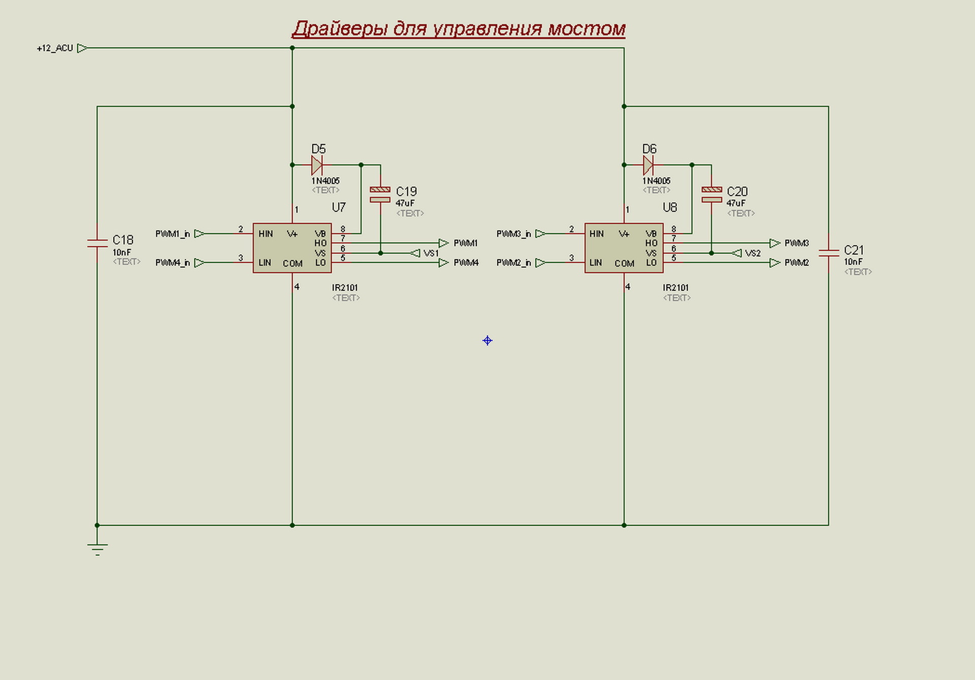
The picture is clickable.
All typical, according to the data on the driver IRS2101S.
Scheme of the formation of impulses of the bridge
In order not to load the MC with useless work, the formation of signals of the bridge pulses is collected on logic I. Three signals are required from the MC. One sinusoidal PWM for the period, as well as two discrete signals, the first half-wave and the second. The implementation of this approach is shown in the figure.

The picture is clickable.
Overcurrent, wound up in the MC and duplicated LED. P-channel transistor control is organized on a bipolar NPN transistor.
The logic of the bridge will be as follows. 20 kHz PWM will be modulated by the sine table in the amount of 400 values. The transfer of values to the PWM register will be organized through DMA. After loading half of the buffer, i.e. 200 values, of one half period, DMA will cause an interrupt, where the signals MCU_P_1 and MCU_P_2 will be mutually inverted. After loading the entire buffer, in the DMA interrupt, the reverse inversion of the signals MCU_P_1 and MCU_P_2 will occur. And further in a cyclic mode. The constant half-wave level will be fed to the upper transistor of the shoulder, and the sinusoidal PWM to the lower key of the opposite shoulder. The next half cycle is another pair of transistors.
During an overcurrent, the NPN transistor Q7 will provide a low level at the input of the logic, which in turn will lead to a low level at the output of the logic and, as a result, the locking of ALL bridge transistors.
Hardware platform
A three-volt bus will power the “brains” of the device - the MK STM32F100C8T6B.
As mentioned above, the MK will be from ST of the STM32 family. What is the reason for this choice?
- MK has a low cost. Analogs on opportunities from ATMEL or PIC have even higher prices, with a bit of 8 bits.
- The presence on board of a 12-bit ADC, DAC, DMA controller.
- 32 bit kernel capacity.
- Increased capacity of program and data memory.
In a word wins in many positions.
To indicate the operation of the device and output the necessary data in the scheme, the sign-based LCD will be used with the control controller KS0066 (HD44780). Libraries for working with such a display in RuNet are full.
The display connection to the controller is as follows.
The picture is clickable.
Connection is direct. Ports MK directly connected to the display. The conjugation of 3 volt and 5 volt logic was not made. There may be problems, and you have to configure the MK outputs as open-collector outlets, and pull up the lines to 5 volts, and the MK outputs themselves use tolerant to 5 volts. As they say, life will show, but when designing a printed circuit board, it is necessary to make this “update”.
Custom buttons are needed to organize navigation through the menus and parameters displayed on the display.
Additional calculations
To calculate the bootstrap capacitor, we use the method proposed in this article . At the end of the description there is an example of calculating the required capacity of the bootstrap capacitor. Take it as a basis and recalculate for our realities.
We define the parameters of the scheme:
- V IN, MAX = 15V maximum input voltage,
- V DRV = 12V driver supply voltage and the amplitude of the control signal,
- dV BST = 0.5V voltage ripple on capacitor C BST in steady state,
- dV BST, MAX = 3V maximum voltage drop on C BST before the undervoltage protection circuit works or the amplitude of the control signal becomes insufficient,
- f DRV = 100 Hz conversion frequency, since our capacitor operates in the interval of 10 ms,
- D MAX = 1 maximum fill factor at minimum input voltage.
Characteristics of the components used:
- Q G = 24 nC total switching charge IRLZ44ZS with V DRV = 5V and V DS = 44V,
- R GS = 10K the value of the resistor R GS ,
- I R = 10uA the leakage current of the diode D BST at the maximum input voltage and its transition temperature TJ = 80 ° C,
- V F = 0.6V voltage drop across the diode D BST at a current of 0.1A and a transition temperature TJ = 80 ° C,
- I LK = 0.13mA level leakage current at the maximum input voltage and crystal temperature TJ = 100 ° C,
- I QBS = 1mA current consumed by the top level driver.
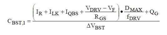

The calculated value is selected from the standard series. The type of capacitor we take tantalum, to reduce the leakage current of the capacitor itself. The total is 47 microfarads x 25 V, type D.
Calculate the charge current of the capacitor, thereby pick up the diode.

So the diode is designed for a direct current of 1 A, will cope with this task.
Conclusion
This article has developed the RIP circuitry. Now all the pieces of the scheme put together. And based on the already approved scheme, we will develop the topology of the printed circuit board. The layout of the printed circuit board and the generalized electrical circuit with a specification for the components will be presented in the next article.
Software implementation of the functional device will sign in a separate article. There is an idea to implement many interesting solutions in the program, for example, PID regulation of the output voltage when operating from the battery.
Epilogue
With this article, I wanted to bring to the public and experienced radio amateurs and non-lovers, too, schematic decisions. Perhaps the attentive reader will find any critical errors in the circuit design or suggest a more correct execution of individual nodes. There will be some simpler solution of the nodes or to improve the reliability to introduce additional circuit solutions.
PS
Links to all parts of the cycle:
- Development of a low-power backup power source with a sine output. Part 1. Statement of the problem.
- Development of a low-power backup power source with a sine output. Part 2. Development of electrical concepts.
- Development of a low-power backup power source with a sine output. Part 3. Work on the bugs
Source: https://habr.com/ru/post/390325/
All Articles