The development of video cards in the 2000s
Continuing the history of the development of video cards from the previous one - articles , video adapters of the 2000s.
VSA-100 chipset (Voodoo Scalable Architecture - scalable Voodoo architecture) was released by 3dfx in June 2000. The first video card to use this chip (VSA-100x2) was the Voodoo5 5500. Made using a 250-nm process technology, with 14 million transistors. The amount of memory SDRAM reached 64 MB, with a 128-bit bus. The frequency of the graphics processor and memory was 166 MHz. For the first time, Voodoo supported 32-bit color in 3D, as well as high-resolution textures of 2048x2048 pixels. FXT1 and DXTC algorithms were used for compression. A feature of the Voodoo5 5500 was high performance when using anti-aliasing.
')
The video card was produced with different interfaces, such as AGP, PCI, etc. There was also a Macintosh version available, with two connectors (DVI and VGA).
In the autumn of the same year, 3dfx released Voodoo4 4500 with 32 MB of memory, which used one VSA-100 chip. The model turned out to be rather slow and significantly inferior to the GeForce 2 MX and Radeon SDR.
3Dfx announced the release of a high-performance Voodoo5 6000 video card on 4 VSA-100 chips and with 128 MB of memory. But it was not possible to finally implement the project - serious financial difficulties bankrupted 3Dfx.
In 2000-2001, NVIDIA released the GeForce 2 video card series (GTS, Ultra, Pro, MX, etc.). These video adapters had a 256-bit core - one of the most productive cores of that time.
The base model was GeForce 2 GTS (GigaTexel Shading), codename NV15. This video card was manufactured using the 180-nm process technology and contained 25 million transistors. The amount of DDR SGRAM memory was 32 MB or 64 MB with a frequency of 200 MHz and a 128-bit bus. The adapter had 4 pixel pipelines. NV15 included full support for DirectX 7, OpenGL 1.2, as well as hardware processing of geometry and lighting (T & L).
ATI did not lag behind the progress and in 2000 released the Radeon R100 processor (originally called the Rage 6). It was manufactured using the 180-nm process technology and supported ATI HyperZ technology.
Based on the R100, the Radeon DDR and SDR video cards were released.

Radeon DDR was released with a video memory of 32 MB or 64 MB. The core and memory frequencies were 183 MHz, a 128-bit bus was used. The interface was AGP 4x. The video card had 2 pixel pipelines.
The simplified version of the SDR differed from the Radeon DDR in the type of memory used and in the lower frequencies (166 MHz). The memory capacity of the Radeon SDR was provided only for 32 MB.
In 2001, two Radeon 8500 and Radeon 7500 chips came out on the basis of the RV200.

The latest developments of ATI were collected in the Radeon 8500, it turned out to be very fast. Made on the 150-nm process technology, contains 60 million transistors. The core and memory frequencies were 275 MHz. Used 128-bit bus. DDR SDRAM memory was offered in two versions: 64 MB and 128 MB. Pixel pipelines were 4.
Radeon 7500 was made on the same 150-nm process technology, but with 30 million transistors. The core worked at 290 MHz, and the memory at 230 MHz. Pixel pipelines were 2.

In 2001, GeForce 3 GPUs codenamed NV20 were released. The processor was released on the 150-nm process technology. The amount of memory offered at 64 MB and 128 MB. The bus was 128-bit and consisted of four 32-bit controllers. The core worked at 200 MHz, and the memory at 230 MHz. There were 4 pixel pipelines. Productivity was 800 billion operations / sec. Memory bandwidth was 7.36 GB / s
The device supported nFinite FX Engine, allowing you to create a huge number of different special effects. There was an improved LMA (Lightspeed Memory Architecture) memory architecture.
The line of video cards consisted of modifications of GeForce 3, GeForce 3 Ti 200 and Ti 500. They differed in clock frequency, performance and memory bandwidth.
The GeForce 3 Ti 200: 175 MHz core, 200 MHz memory; 700 billion operations / sec; 6.4 GB / s bandwidth.

The GeForce 3 Ti 500: 240 MHz core and 250 MHz memory; 960 billion operations / sec; 8.0 Gb / s bandwidth.
The next video card from NVIDIA was GeForce 4, which was released in 2002. With this name, two types of graphic cards were produced: high-performance Ti (Titanium) and low-cost MX.

The GeForce 4 Ti line was represented by the Ti 4400, Ti 4600, and Ti 4200 models. The video cards differed in core and memory clock frequencies. The amount of video memory was 128 MB (a variant of 64 MB was offered for the Ti 4200). Titanium used a 128-bit 4-channel memory controller with LightSpeed Memory Architecture II, there were 4 rendering blocks, 8 texture units, 2 T & L, Accuview anti-aliasing subsystem and nFiniteFX II shader engine, providing full support for DirectX 8.1 and OpenGL 1.3. The GeForce 4 Ti 4200 model was the most widespread due to high performance at an affordable price.
GeForce 4 MX inherited the architecture of GeForce 2 (with increased speed). They were based on the NV17 chip, manufactured using the 150-nm process technology and consisting of 27 million transistors. The amount of video memory was 64 MB. The GPU had 2 rendering units, 4 texture units, 1 T & L unit, 128-bit 2-channel memory controller with LightSpeed Memory Architecture II. The chip also had an Accuview anti-aliasing subsystem.
In the summer of 2002, ATI released the R300 chip, which was manufactured using the 150-nm process technology and contained about 110 million transistors. He had 8 pixel pipelines. The chip also supported improved smoothing methods.
Based on the R300, the Radeon 9700 graphics card with a core clock frequency of 325 MHz and 310 MHz memory was released. The memory capacity was 128 MB. The memory bus was 256-bit DDR.
In early 2003, the Radeon 9700 was replaced by the Radeon 9800 video card. The new solutions were built on the R350 chip, with an increase in clock frequencies and refinement of the shader units, the memory controller.
GeForce FX is the fifth generation of graphics processors developed and manufactured by NVIDIA from the end of 2002 to 2004. One of the first video cards of the GeForce FX series had improved methods for anti-aliasing and anisotropic filtering. She supported vertex and pixel shaders version 2.0. Thanks to the 64-bit and 128-bit color representation, the quality of bright images has improved. The NV30 chip was manufactured on a 130-nm process technology and worked with a 128-bit AGP 8x bus, supporting DDR2 memory.
GeForce FX was presented in different versions: extension-level (5200, 5300, 5500), mid-range (5600, 5700, 5750), high-end (5800, 5900, 5950), enthusiast (5800 Ultra, 5900 Ultra, 5950 Ultra). Used bus on 126-bit and 256-bit.
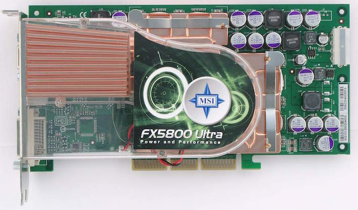
Based on the NV30, a top-end device of the new generation was created - the GeForce FX 5800 video card. The video memory reached 256 MB, the core frequency was 400 MHz, and the memory was 800 MHz. In the 5800 Ultra, the core frequency increased to 500 MHz, and the memory to 1000 MHz. The first NV30-based cards were equipped with an innovative cooling system.
The development of video cards actively continued, and in 2004 the next product of the company was released - GeForce 6 Series (codenamed NV40).
The NV40 chip was also produced on the 130-nm process technology, which did not prevent it from becoming more economical. The modification of pixel pipelines made it possible to handle up to 16 pixels per clock. There were a total of 16 pixel pipelines. The video cards supported pixel and vertex shaders version 3.0, UltraShadow technology (shadow rendering). In addition, GeForce 6 Series using PureVideo technology decoded video formats H.264, VC-1 and MPEG-2. The NV40 worked through a 256-bit bus, using very fast GDDR3 memory modules.
One of the first models, the GeForce 6800 video card was very productive and pulled the newest games of that time. It worked both through the AGP interface and through the PCI Express bus. The core frequency was 325 MHz, and the memory frequency was 700 MHz. Memory capacity reached 256 MB or 512 MB.
ATI was in a better position. In 2004, the company introduced a 130 nm R420 chip (an upgraded version of the R300). Pixel pipelines were divided into four blocks of four pipelines each (a total of 16 pixel pipelines). Increased to 6 the number of vertex conveyors. Since the R420 did not support third-generation shaders, it worked with the updated HyperZ HD technology.
The most powerful and productive video card of the new Radeon line was the X800 XT. The card was equipped with a 256 MB GDDR3 memory and 256-bit bus width. The frequency of operation reached 520 MHz in the core and 560 MHz in memory. The Radeon X800 XT was sold in two versions: AGP and PCI Express. In addition to the standard version, there was the Radeon X800 XT Platinum Edition, which has higher chip and memory frequencies.
In 2005, the G70 chip came out, which became the basis for GeForce 7800 series video cards. The number of transistors increased to 302 million.
The number of pixel pipelines has doubled - to 24 pieces. Additional ALU blocks were added to each pipeline, which are responsible for processing the most popular pixel shaders. Thus, the performance of the chip has increased in games that emphasize the performance of pixel processors.
GeForce 7800 GTX is the first video card based on the G70. The core frequency was 430 MHz, the memory - 600 MHz. Used fast GDDR3, as well as a 256-bit bus. Memory capacity was 256 MB or 512 MB. The GeForce 7800 GTX worked exclusively through the PCI Express x16 interface, which finally began to supplant the aging AGP.
The 2006 event for NVIDIA was the release of the first dual-GPU GeForce 7950 graphics card based on the 90-nm process technology. The NVIDIA 7950 GX2 had one G71 chip on each of the boards. The cores of the video card ran at 500 MHz, the memory at 600 MHz. The amount of video memory type GDDR3 was 1 GB (512 MB for each chip), 256-bit bus.
The new card optimized power consumption and improved the cooling system. The release of the 7950 GX2 was the beginning of the development of Quad SLI technology, which allows simultaneously using the power of several video cards for processing three-dimensional images.
Based on the R520, the Radeon X1800 XT graphics card was developed. The card was equipped with 256 MB or 512 MB of GDDR3 memory operating at 750 MHz. A 256-bit bus was used.

Radeon X1800 XT video cards did not last long on the market. Soon they were replaced by adapters of the Radeon X1900 XTX series based on the R580 chip. The processor was fully supported on the hardware level of the SM 3.0 specification (DirectX 9.0c) and HDR-blending in FP16 format with MSAA sharing. In the new chip, the number of pixel pipelines was increased to 48. The core frequency was 650 MHz, and the memory - 775 MHz.
Six months later, the R580 + chip came out with a new memory controller that works with the GDDR4 standard. The memory frequency was increased to 2000 MHz, while the bus remained 256-bit. The main characteristics of the chip remained the same: 48 pixel pipelines, 16 texture and 8 vertex pipelines. The core frequency was 625 MHz, the memory was more - 900 MHz.
In 2006, based on the G80 processor, several video cards were released, the most powerful of which was the GeForce 8800 GTX. The G80 was one of the most complex chip in existence at the time. It was produced on the 90-nm process technology and contained 681 million transistors. The core worked at a frequency of 575 MHz, the memory at a frequency of 900 MHz. The frequency of unified shader units was 1350 MHz. The GeForce 8800 GTX had 768 MB of GDDR3 video memory, and the bus width was 384-bit. New anti-aliasing techniques were supported, which allowed ROPs to work with HDR light in MSAA mode (Multisample anti-aliasing). Received the development of technology PureVideo.
The architecture of the GeForce 8800 GTX proved to be particularly efficient and for several years was one of the fastest graphics cards.
In 2007, the flagship Radeon HD2900 XT video card based on the R600 chip was introduced. The core frequency of the video card was 740 MHz, GDDR4 memory - 825 MHz. A 512-bit memory bus was used. The amount of video memory reached 512 MB and 1 GB.
A more successful development was the RV670 processor, released in the same year. The architecture did not differ much from its predecessor, but it was manufactured using the 55-nm process technology and with a 256-bit memory bus. Added support for DirectX 10.1 and Shader Model 4.1. Based on the processor, Radeon HD 3870 video cards (775 MHz core frequency, 1125 MHz memory) and Radeon HD 3850 (670 MHz core frequency, 828 MHz memory) were produced with 256 MB of video memory and 512 MB and a 256-bit bus.
The G92 chip formed the basis of the GeForce 9800 GTX - one of the fastest and most affordable graphics cards. It was made on the 65-nm process technology. The core frequency was 675 MHz, the memory frequency was 1100 MHz, and the bus was 256-bit. The memory capacity was offered in two versions: 512 MB and 1 GB. A little later, the GTX + model appeared, which differed in the 55-nm process technology and the core frequency - 738 MHz.
The next dual-chip GeForce 9800 GX2 graphics card also appeared in this line. Each of the processors had specifications like that of the GeForce 8800 GTS 512 MB, but with different frequencies.
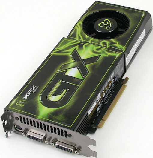
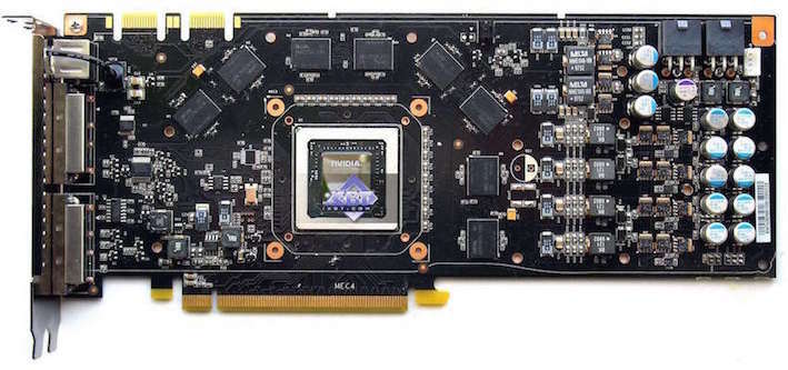
In 2008, NVIDIA released the GT200 chip, which was used in GeForce GTX 280 and GTX 260 video cards. The chip was manufactured using the 65-nm process technology and contained 1.4 billion transistors, 32 ROPs and 80 texture units. Memory bus increased to 512-bit. Support for the PhysX physics engine and the CUDA platform has also been added. The core frequency of the video card was 602 MHz, and GDDR3 memory - 1107 MHz.
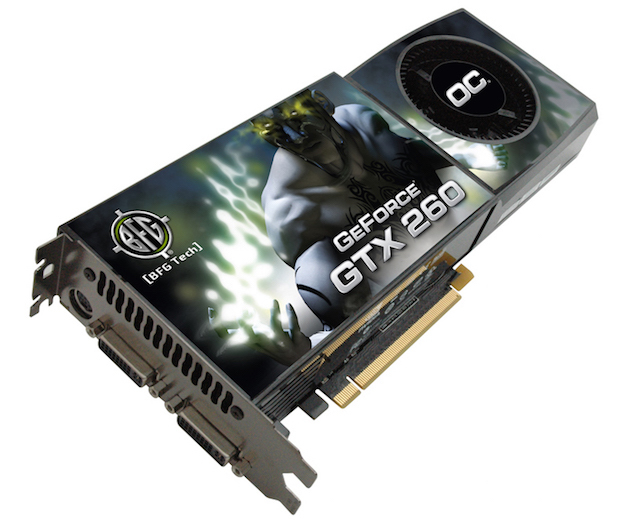
The GeForce GTX 260 uses a 448-bit GDDR3 bus. The core frequency reached 576 MHz, and the memory - 999 MHz.
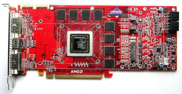
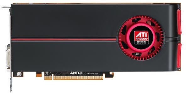
The older video card is called the Radeon HD 4870. The core frequency was 750 MHz, and the memory worked at the effective frequency of 3600 MHz. With the new line of video cards, the company continued its new release policy for devices that could successfully compete in the Middle-End segment. So, the Radeon HD 4870 became a worthy competitor to the GeForce GTX 260 video card. And the leader in the HD 4000 line soon became the next two-chip Radeon HD 4870X2 solution. The architecture of the video card corresponded to that of the Radeon HD 3870X2, not counting the presence of the Sideport interface, which directly connects the two cores for the most rapid exchange of information.
In 2010, NVIDIA introduced the GF100 with the architecture of Fermi, which formed the basis for the GeForce GTX 480 video card. The GF100 was produced using a 40-nm process technology and received 512 stream processors. The core frequency was 700 MHz, and the memory - 1848 MHz. The bus width was 384-bit. GDDR5 video memory reached 1.5 GB.
Chip GF100 supported DirectX 11 and Shader Model 5.0, as well as the new technology NVIDIA Surround, allowing you to deploy applications on three screens, thereby creating the effect of complete immersion.
AMD has released a 40-nm Cypress chip. The developers of the company decided to change the approach and not to use exclusively alphanumeric values. Generation chips began to assign their own names. The very principle of the Cypress architecture continued the ideas of the RV770, but the design was reworked. The number of stream processors, texture modules and ROP blocks has doubled. There is support for DirectX 11 and Shader Model 5.0. In Cypress, new texture compression methods have been introduced that allowed developers to use larger textures. Also, AMD introduced the new technology Eyefinity, the full analogue of which later became NVIDIA Surround technology.
The Cypress chip was implemented in the Radeon HD 5000 series of graphics cards. Soon, AMD also released the Radeon HD 5970 dual-chip solution. In general, Cypress was very successful.
The Radeon HD 6000 series of video cards, released at the end of 2010, was designed to compete with the GeForce GTX 500 accelerators. The Cayman chip was at the core of graphics adapters. It used a slightly different VLIW4 architecture. The number of stream processors was 1536 units. The number of texture modules has increased - there are 96 of them. Cayman also knew how to work with the new Enhanced Quality AA smoothing algorithm. The memory bus width of the chip was 256-bit. Video cards used GDDR5 memory.
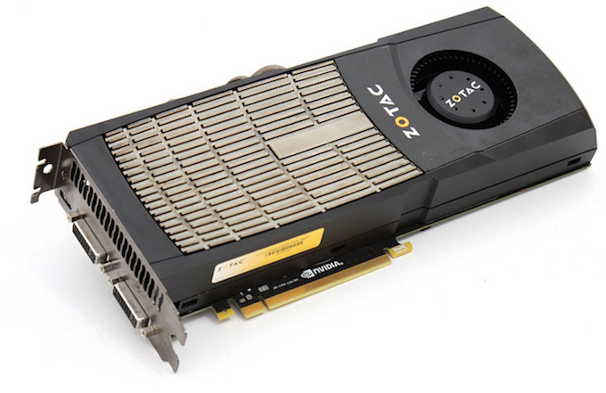
Since 2011, NVIDIA has released a generation of graphics accelerators. One of the notable models was the video card GeForce GTX 680, based on the GK104 chip, produced by the 28-nm process technology. The core frequency is 1006 MHz, the memory frequency is 6008 MHz, the 256-bit GDDR5 bus.
In 2013, the company introduced the GK110 chip, on which the flagship GeForce GTX 780 and GeForce GTX Titan video cards are based. The 384-bit GDDR5 bus was used, and the memory capacity increased to 6 GB.
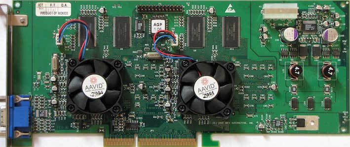
VSA-100 and the new generation of Voodoo
VSA-100 chipset (Voodoo Scalable Architecture - scalable Voodoo architecture) was released by 3dfx in June 2000. The first video card to use this chip (VSA-100x2) was the Voodoo5 5500. Made using a 250-nm process technology, with 14 million transistors. The amount of memory SDRAM reached 64 MB, with a 128-bit bus. The frequency of the graphics processor and memory was 166 MHz. For the first time, Voodoo supported 32-bit color in 3D, as well as high-resolution textures of 2048x2048 pixels. FXT1 and DXTC algorithms were used for compression. A feature of the Voodoo5 5500 was high performance when using anti-aliasing.
')
The video card was produced with different interfaces, such as AGP, PCI, etc. There was also a Macintosh version available, with two connectors (DVI and VGA).
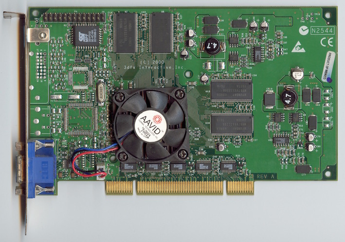
In the autumn of the same year, 3dfx released Voodoo4 4500 with 32 MB of memory, which used one VSA-100 chip. The model turned out to be rather slow and significantly inferior to the GeForce 2 MX and Radeon SDR.
3Dfx announced the release of a high-performance Voodoo5 6000 video card on 4 VSA-100 chips and with 128 MB of memory. But it was not possible to finally implement the project - serious financial difficulties bankrupted 3Dfx.
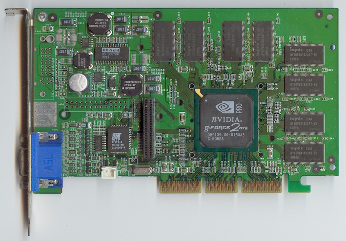
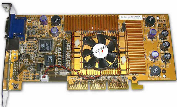
Geforce 2
In 2000-2001, NVIDIA released the GeForce 2 video card series (GTS, Ultra, Pro, MX, etc.). These video adapters had a 256-bit core - one of the most productive cores of that time.
The base model was GeForce 2 GTS (GigaTexel Shading), codename NV15. This video card was manufactured using the 180-nm process technology and contained 25 million transistors. The amount of DDR SGRAM memory was 32 MB or 64 MB with a frequency of 200 MHz and a 128-bit bus. The adapter had 4 pixel pipelines. NV15 included full support for DirectX 7, OpenGL 1.2, as well as hardware processing of geometry and lighting (T & L).
Radeon DDR and SDR
ATI did not lag behind the progress and in 2000 released the Radeon R100 processor (originally called the Rage 6). It was manufactured using the 180-nm process technology and supported ATI HyperZ technology.
Based on the R100, the Radeon DDR and SDR video cards were released.
Radeon DDR was released with a video memory of 32 MB or 64 MB. The core and memory frequencies were 183 MHz, a 128-bit bus was used. The interface was AGP 4x. The video card had 2 pixel pipelines.
The simplified version of the SDR differed from the Radeon DDR in the type of memory used and in the lower frequencies (166 MHz). The memory capacity of the Radeon SDR was provided only for 32 MB.
Radeon 8500 and Radeon 7500
In 2001, two Radeon 8500 and Radeon 7500 chips came out on the basis of the RV200.
The latest developments of ATI were collected in the Radeon 8500, it turned out to be very fast. Made on the 150-nm process technology, contains 60 million transistors. The core and memory frequencies were 275 MHz. Used 128-bit bus. DDR SDRAM memory was offered in two versions: 64 MB and 128 MB. Pixel pipelines were 4.
Radeon 7500 was made on the same 150-nm process technology, but with 30 million transistors. The core worked at 290 MHz, and the memory at 230 MHz. Pixel pipelines were 2.
Geforce 3
In 2001, GeForce 3 GPUs codenamed NV20 were released. The processor was released on the 150-nm process technology. The amount of memory offered at 64 MB and 128 MB. The bus was 128-bit and consisted of four 32-bit controllers. The core worked at 200 MHz, and the memory at 230 MHz. There were 4 pixel pipelines. Productivity was 800 billion operations / sec. Memory bandwidth was 7.36 GB / s
The device supported nFinite FX Engine, allowing you to create a huge number of different special effects. There was an improved LMA (Lightspeed Memory Architecture) memory architecture.
The line of video cards consisted of modifications of GeForce 3, GeForce 3 Ti 200 and Ti 500. They differed in clock frequency, performance and memory bandwidth.
The GeForce 3 Ti 200: 175 MHz core, 200 MHz memory; 700 billion operations / sec; 6.4 GB / s bandwidth.
The GeForce 3 Ti 500: 240 MHz core and 250 MHz memory; 960 billion operations / sec; 8.0 Gb / s bandwidth.
GeForce 4
The next video card from NVIDIA was GeForce 4, which was released in 2002. With this name, two types of graphic cards were produced: high-performance Ti (Titanium) and low-cost MX.
The GeForce 4 Ti line was represented by the Ti 4400, Ti 4600, and Ti 4200 models. The video cards differed in core and memory clock frequencies. The amount of video memory was 128 MB (a variant of 64 MB was offered for the Ti 4200). Titanium used a 128-bit 4-channel memory controller with LightSpeed Memory Architecture II, there were 4 rendering blocks, 8 texture units, 2 T & L, Accuview anti-aliasing subsystem and nFiniteFX II shader engine, providing full support for DirectX 8.1 and OpenGL 1.3. The GeForce 4 Ti 4200 model was the most widespread due to high performance at an affordable price.
GeForce 4 MX inherited the architecture of GeForce 2 (with increased speed). They were based on the NV17 chip, manufactured using the 150-nm process technology and consisting of 27 million transistors. The amount of video memory was 64 MB. The GPU had 2 rendering units, 4 texture units, 1 T & L unit, 128-bit 2-channel memory controller with LightSpeed Memory Architecture II. The chip also had an Accuview anti-aliasing subsystem.
Radeon 9700 pro
In the summer of 2002, ATI released the R300 chip, which was manufactured using the 150-nm process technology and contained about 110 million transistors. He had 8 pixel pipelines. The chip also supported improved smoothing methods.
Based on the R300, the Radeon 9700 graphics card with a core clock frequency of 325 MHz and 310 MHz memory was released. The memory capacity was 128 MB. The memory bus was 256-bit DDR.
In early 2003, the Radeon 9700 was replaced by the Radeon 9800 video card. The new solutions were built on the R350 chip, with an increase in clock frequencies and refinement of the shader units, the memory controller.
Geforce fx
GeForce FX is the fifth generation of graphics processors developed and manufactured by NVIDIA from the end of 2002 to 2004. One of the first video cards of the GeForce FX series had improved methods for anti-aliasing and anisotropic filtering. She supported vertex and pixel shaders version 2.0. Thanks to the 64-bit and 128-bit color representation, the quality of bright images has improved. The NV30 chip was manufactured on a 130-nm process technology and worked with a 128-bit AGP 8x bus, supporting DDR2 memory.
GeForce FX was presented in different versions: extension-level (5200, 5300, 5500), mid-range (5600, 5700, 5750), high-end (5800, 5900, 5950), enthusiast (5800 Ultra, 5900 Ultra, 5950 Ultra). Used bus on 126-bit and 256-bit.
Based on the NV30, a top-end device of the new generation was created - the GeForce FX 5800 video card. The video memory reached 256 MB, the core frequency was 400 MHz, and the memory was 800 MHz. In the 5800 Ultra, the core frequency increased to 500 MHz, and the memory to 1000 MHz. The first NV30-based cards were equipped with an innovative cooling system.
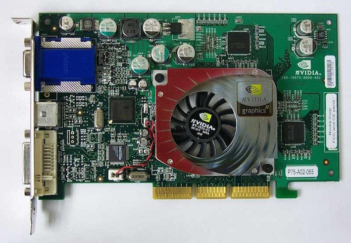
GeForce 6 Series
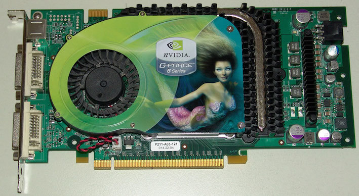
The development of video cards actively continued, and in 2004 the next product of the company was released - GeForce 6 Series (codenamed NV40).
The NV40 chip was also produced on the 130-nm process technology, which did not prevent it from becoming more economical. The modification of pixel pipelines made it possible to handle up to 16 pixels per clock. There were a total of 16 pixel pipelines. The video cards supported pixel and vertex shaders version 3.0, UltraShadow technology (shadow rendering). In addition, GeForce 6 Series using PureVideo technology decoded video formats H.264, VC-1 and MPEG-2. The NV40 worked through a 256-bit bus, using very fast GDDR3 memory modules.
One of the first models, the GeForce 6800 video card was very productive and pulled the newest games of that time. It worked both through the AGP interface and through the PCI Express bus. The core frequency was 325 MHz, and the memory frequency was 700 MHz. Memory capacity reached 256 MB or 512 MB.
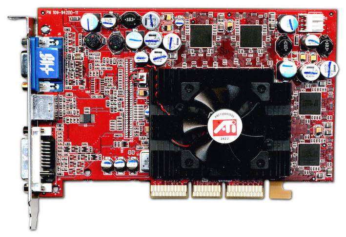
Radeon X800 XT
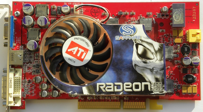
ATI was in a better position. In 2004, the company introduced a 130 nm R420 chip (an upgraded version of the R300). Pixel pipelines were divided into four blocks of four pipelines each (a total of 16 pixel pipelines). Increased to 6 the number of vertex conveyors. Since the R420 did not support third-generation shaders, it worked with the updated HyperZ HD technology.
The most powerful and productive video card of the new Radeon line was the X800 XT. The card was equipped with a 256 MB GDDR3 memory and 256-bit bus width. The frequency of operation reached 520 MHz in the core and 560 MHz in memory. The Radeon X800 XT was sold in two versions: AGP and PCI Express. In addition to the standard version, there was the Radeon X800 XT Platinum Edition, which has higher chip and memory frequencies.
GeForce 7800 GTX
In 2005, the G70 chip came out, which became the basis for GeForce 7800 series video cards. The number of transistors increased to 302 million.
The number of pixel pipelines has doubled - to 24 pieces. Additional ALU blocks were added to each pipeline, which are responsible for processing the most popular pixel shaders. Thus, the performance of the chip has increased in games that emphasize the performance of pixel processors.
GeForce 7800 GTX is the first video card based on the G70. The core frequency was 430 MHz, the memory - 600 MHz. Used fast GDDR3, as well as a 256-bit bus. Memory capacity was 256 MB or 512 MB. The GeForce 7800 GTX worked exclusively through the PCI Express x16 interface, which finally began to supplant the aging AGP.
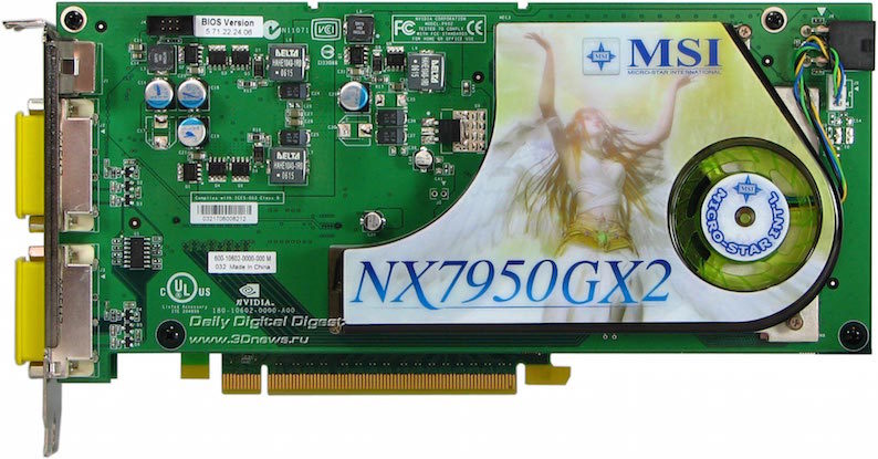
GeForce 7950 GX2
The 2006 event for NVIDIA was the release of the first dual-GPU GeForce 7950 graphics card based on the 90-nm process technology. The NVIDIA 7950 GX2 had one G71 chip on each of the boards. The cores of the video card ran at 500 MHz, the memory at 600 MHz. The amount of video memory type GDDR3 was 1 GB (512 MB for each chip), 256-bit bus.
The new card optimized power consumption and improved the cooling system. The release of the 7950 GX2 was the beginning of the development of Quad SLI technology, which allows simultaneously using the power of several video cards for processing three-dimensional images.
Radeon X1800 XT, X1900
Based on the R520, the Radeon X1800 XT graphics card was developed. The card was equipped with 256 MB or 512 MB of GDDR3 memory operating at 750 MHz. A 256-bit bus was used.
Radeon X1800 XT video cards did not last long on the market. Soon they were replaced by adapters of the Radeon X1900 XTX series based on the R580 chip. The processor was fully supported on the hardware level of the SM 3.0 specification (DirectX 9.0c) and HDR-blending in FP16 format with MSAA sharing. In the new chip, the number of pixel pipelines was increased to 48. The core frequency was 650 MHz, and the memory - 775 MHz.
Six months later, the R580 + chip came out with a new memory controller that works with the GDDR4 standard. The memory frequency was increased to 2000 MHz, while the bus remained 256-bit. The main characteristics of the chip remained the same: 48 pixel pipelines, 16 texture and 8 vertex pipelines. The core frequency was 625 MHz, the memory was more - 900 MHz.
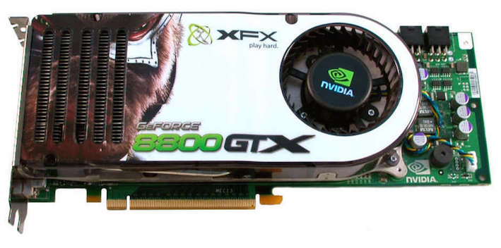
GeForce 8800 GTX
In 2006, based on the G80 processor, several video cards were released, the most powerful of which was the GeForce 8800 GTX. The G80 was one of the most complex chip in existence at the time. It was produced on the 90-nm process technology and contained 681 million transistors. The core worked at a frequency of 575 MHz, the memory at a frequency of 900 MHz. The frequency of unified shader units was 1350 MHz. The GeForce 8800 GTX had 768 MB of GDDR3 video memory, and the bus width was 384-bit. New anti-aliasing techniques were supported, which allowed ROPs to work with HDR light in MSAA mode (Multisample anti-aliasing). Received the development of technology PureVideo.
The architecture of the GeForce 8800 GTX proved to be particularly efficient and for several years was one of the fastest graphics cards.
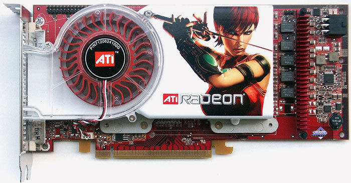
Radeon HD2900 XT, HD 3870 and HD 3850
In 2007, the flagship Radeon HD2900 XT video card based on the R600 chip was introduced. The core frequency of the video card was 740 MHz, GDDR4 memory - 825 MHz. A 512-bit memory bus was used. The amount of video memory reached 512 MB and 1 GB.
A more successful development was the RV670 processor, released in the same year. The architecture did not differ much from its predecessor, but it was manufactured using the 55-nm process technology and with a 256-bit memory bus. Added support for DirectX 10.1 and Shader Model 4.1. Based on the processor, Radeon HD 3870 video cards (775 MHz core frequency, 1125 MHz memory) and Radeon HD 3850 (670 MHz core frequency, 828 MHz memory) were produced with 256 MB of video memory and 512 MB and a 256-bit bus.
GeForce 9800
The G92 chip formed the basis of the GeForce 9800 GTX - one of the fastest and most affordable graphics cards. It was made on the 65-nm process technology. The core frequency was 675 MHz, the memory frequency was 1100 MHz, and the bus was 256-bit. The memory capacity was offered in two versions: 512 MB and 1 GB. A little later, the GTX + model appeared, which differed in the 55-nm process technology and the core frequency - 738 MHz.
The next dual-chip GeForce 9800 GX2 graphics card also appeared in this line. Each of the processors had specifications like that of the GeForce 8800 GTS 512 MB, but with different frequencies.
GeForce GTX 280 and GTX 260
In 2008, NVIDIA released the GT200 chip, which was used in GeForce GTX 280 and GTX 260 video cards. The chip was manufactured using the 65-nm process technology and contained 1.4 billion transistors, 32 ROPs and 80 texture units. Memory bus increased to 512-bit. Support for the PhysX physics engine and the CUDA platform has also been added. The core frequency of the video card was 602 MHz, and GDDR3 memory - 1107 MHz.
The GeForce GTX 260 uses a 448-bit GDDR3 bus. The core frequency reached 576 MHz, and the memory - 999 MHz.
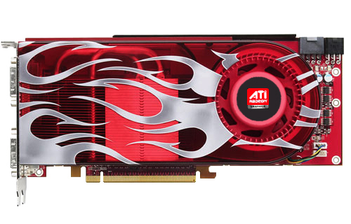
Radeon HD 4870
The older video card is called the Radeon HD 4870. The core frequency was 750 MHz, and the memory worked at the effective frequency of 3600 MHz. With the new line of video cards, the company continued its new release policy for devices that could successfully compete in the Middle-End segment. So, the Radeon HD 4870 became a worthy competitor to the GeForce GTX 260 video card. And the leader in the HD 4000 line soon became the next two-chip Radeon HD 4870X2 solution. The architecture of the video card corresponded to that of the Radeon HD 3870X2, not counting the presence of the Sideport interface, which directly connects the two cores for the most rapid exchange of information.
GeForce GTX 480
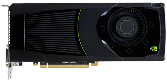
In 2010, NVIDIA introduced the GF100 with the architecture of Fermi, which formed the basis for the GeForce GTX 480 video card. The GF100 was produced using a 40-nm process technology and received 512 stream processors. The core frequency was 700 MHz, and the memory - 1848 MHz. The bus width was 384-bit. GDDR5 video memory reached 1.5 GB.
Chip GF100 supported DirectX 11 and Shader Model 5.0, as well as the new technology NVIDIA Surround, allowing you to deploy applications on three screens, thereby creating the effect of complete immersion.
Cypress and Cayman chips
AMD has released a 40-nm Cypress chip. The developers of the company decided to change the approach and not to use exclusively alphanumeric values. Generation chips began to assign their own names. The very principle of the Cypress architecture continued the ideas of the RV770, but the design was reworked. The number of stream processors, texture modules and ROP blocks has doubled. There is support for DirectX 11 and Shader Model 5.0. In Cypress, new texture compression methods have been introduced that allowed developers to use larger textures. Also, AMD introduced the new technology Eyefinity, the full analogue of which later became NVIDIA Surround technology.
The Cypress chip was implemented in the Radeon HD 5000 series of graphics cards. Soon, AMD also released the Radeon HD 5970 dual-chip solution. In general, Cypress was very successful.
The Radeon HD 6000 series of video cards, released at the end of 2010, was designed to compete with the GeForce GTX 500 accelerators. The Cayman chip was at the core of graphics adapters. It used a slightly different VLIW4 architecture. The number of stream processors was 1536 units. The number of texture modules has increased - there are 96 of them. Cayman also knew how to work with the new Enhanced Quality AA smoothing algorithm. The memory bus width of the chip was 256-bit. Video cards used GDDR5 memory.
GeForce GTX 680
Since 2011, NVIDIA has released a generation of graphics accelerators. One of the notable models was the video card GeForce GTX 680, based on the GK104 chip, produced by the 28-nm process technology. The core frequency is 1006 MHz, the memory frequency is 6008 MHz, the 256-bit GDDR5 bus.
In 2013, the company introduced the GK110 chip, on which the flagship GeForce GTX 780 and GeForce GTX Titan video cards are based. The 384-bit GDDR5 bus was used, and the memory capacity increased to 6 GB.
Source: https://habr.com/ru/post/389989/
All Articles