Configurable logic cells in PIC microcontrollers
The original intent of the article was to describe the Microchip Microcontroller Independent Core Peripherals, but the topic turned out to be quite extensive, so as a first step we will talk about CLC - Configurable Logic Cells (Configurable Logic Cell).
The article (Using Configurable Logic Cells to Control WS2812 LED Tape [ 1 ]) looked at how logical CLC cells of PIC controllers can significantly simplify the task of generating WS2812 driver control signals and implement hardware functions for which a simple microcontroller may miss the software solution. .
The purpose of this article is to become more familiar with configurable logic cells in PIC Microchip microcontrollers, to demonstrate examples of implementations and, if possible, to push the reader to think about using CLC in their projects.
In short, the CLC is one of the parts of the stub .
Part 1. Configurable logic cells in PIC microcontrollers
Part 2. I / O Ports
Part 3. ADC with calculator
Introduction
Description. Configuration options. What can be inputs and outputs
Configurable logical cells CLC are part of the PSI — Core Independent Peripheral (CIP) Peripherals, i.e. the functioning of such peripherals does not depend (almost) on the microcontroller's clock frequency and its state (RUN, IDLE, SLEEP).
Of course, such peripherals are configured by the microcontroller program, but further operation can be independent.
Each cell contains an input multiplexer, logic function, output control, connection to the interrupt controller.
The general scheme of one logical cell is shown in Figure 1.
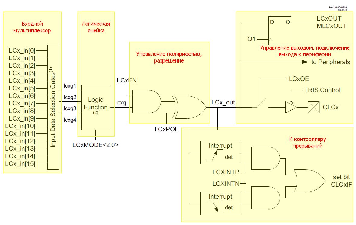
Fig.1. The structure of a single logical cell CLC
Each of the logical cells has 4 inputs, the signals for which are selected by the input multiplexer, each input can be direct or inverse. Part of the inputs may not be used and connected to the level of log.0 or log.1.
Inputs for cells can have external connections (input / output ports) and internal (signals from other peripherals: PWM, comparators, timers, etc., and the outputs of the CLC itself).
The output of the CLC cell has a controlled polarity, it can be connected to the output port of the microcontroller, to other peripherals, to form an interrupt request by changing the state (on the front and / or decay).
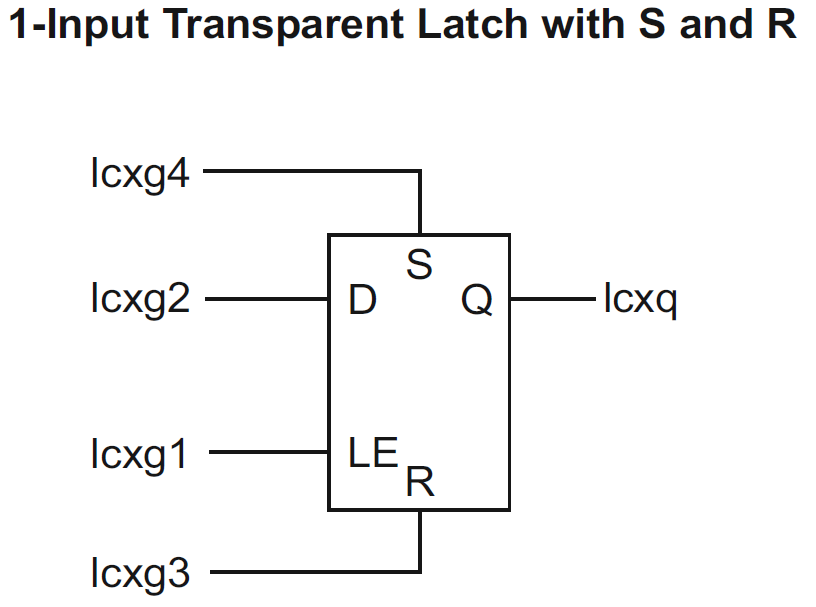
The logical function of each cell is selected from 8 options (see Table 1).
| log cell | log cell |
|---|---|
 |  |
 |  |
 |  |
 |  |
Table 1. Options for logic cell functions.
Since logical cells have a lot of settings, the easiest way to configure CLC is through the MPLAB Code Configurator plugin in the MPLAB X development environment, which creates C configuration files for the enabled peripherals.
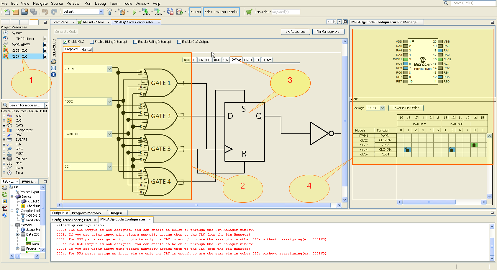
Fig. 2. Mplab X IDE development environment with the Mplab Code Configurator (MCC) plugin launched
Where:
1 - editable cell;
2 - input multiplexer setting and input polarity;
3 - logical cell function;
4 - I / O port redundancy.
Pay attention to the input gates at the CLC input (Fig. 2, p. 2), which are made as 4-OR elements.
If necessary, in accordance with the laws of de Morgan, input gates can be converted from the base OR to AND (see Table 2).
Table 2. Transformation of logical functions
| Logic function | Equivalent representation in CLC |
|---|---|
| 4-OR (OR) |  |
| 4-OR-NOT (NOR) |  |
| 4-AND-NOT (NAND) | 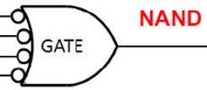 |
| 4-AND (AND) |  |
CLC Usage Examples
Smooth change of LED brightness (flicker)
If the signals of two PWM with similar frequencies are connected to the inputs of a CLC configured as an XOR element (exclusive OR), then the LED blinking (periodic variation of the duty cycle) can be organized. At the same time, the solution is completely hardware and does not require the participation of the MK kernel (program).
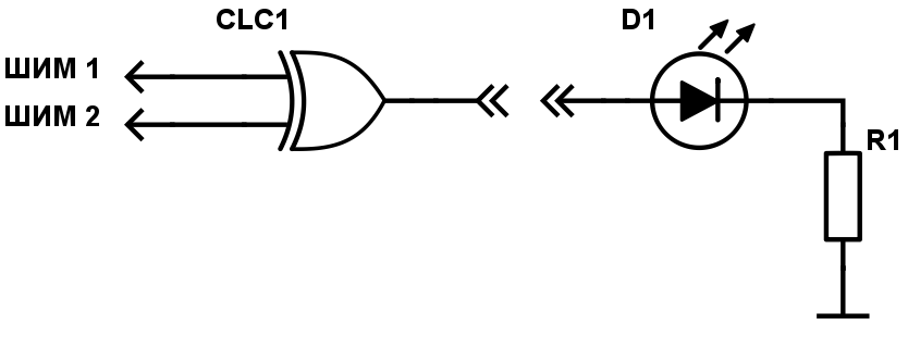
Fig. 3a. Scheme "PWM modulator"
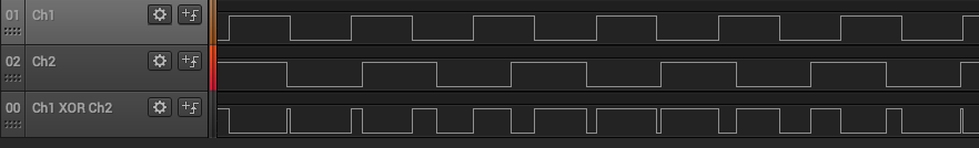
Fig. 3b. Diagrams showing the principle of changing the duty cycle
If it’s a pity to use two PWM modules for such a simple task, then implementation options without PWM are possible:
A) Use overflow signals of two timers (events), plus three CLC cells.
On two JK-triggers in the counting mode, we send signals from the timers (postscaled out) - we get the meanders at the output, which are then sent to the XOR element.
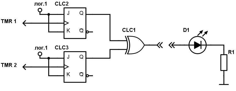
Fig. 3c. Implementation of PWM modulator without input PWM signals
B) Use overflow signals of two timers and one CLC.
We send signals from the Timer (postscaled out) to the RS trigger inputs - we get “sawtooth PWM” at the output (Fig. 3e).
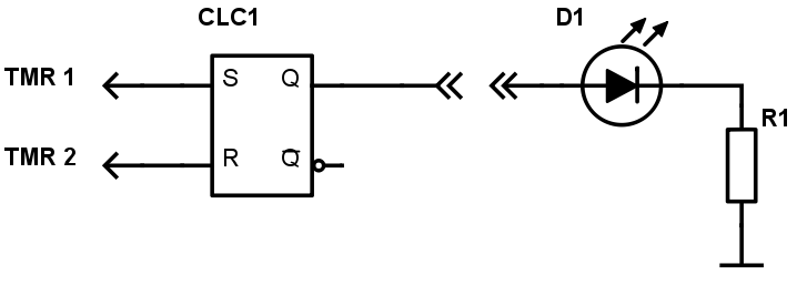
Fig. 3d

Fig. 3e.
Frequency divider
The diagram of the frequency divider by 2 is shown in Fig. 4a. One D-trigger is used in counting mode. The input signal is fed to the clock input, input D is connected to the inverse output of the trigger. At the moment of arrival at the clocking input, the front at input D will always have an inverse signal relative to the current state of the trigger, i.e. the state of the trigger will change only on the front of the input signal.
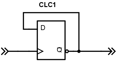
Fig.4a. Divider by 2.
In the MPLAB Code Configurator plugin, this scheme may look like this:
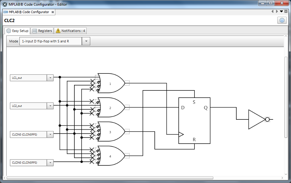
Fig. 4b. Divider by 2 in MCC settings.
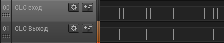
Fig.4c. Diagram of the input and output of the divider.
The divider by 3 is shown in Fig. 4d.
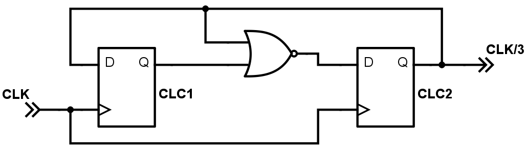
Fig. 4d. Divider by 3.
The divisor by 4 is two consecutive divisors by 2 ;-)
Where can dividers be used? Where you need to divide the frequency.
The following example uses frequency dividers.
Stepper motor driver
One of the easiest options for controlling a Stepper Motor (SM) is full-step control. In this embodiment, the control signals are shifted by 90 °. Therefore, it is possible to take a periodic signal, for one frequency divider to submit it directly, and for the other, in the inverse one.
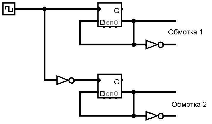
Fig. 5a. Shaper control signals stepper motor.
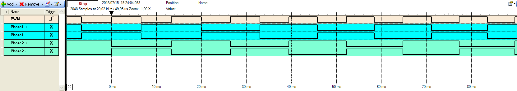
Fig. 5b. The diagram at the shaper output.
Changing the frequency at the CLC input will change the frequency of the stepper motor control signals. The input frequency can be taken from the input of the microcontroller (external signal), or from an internal source - PWM or NCO generator.
When controlling PWM, 2 parameters need to be changed: the period register (frequency) and the duty ratio register, since the control signal must have a 50% duty cycle.
The use of NCO (Numerically Controlled Oscillator, controlled oscillator) looks more attractive, since this generator can automatically generate a meander, therefore, to change the frequency, you only need to change the values in one register.
To change direction, you need to invert the signals on one of the phases.
Delay. Formation of impulse on the front, decline, changes
For some tasks it may be necessary to form a delayed pulse.
To do this, you can use the D-trigger. We feed the input signal to the counting input, or a high-frequency signal (for example, the Fosc clock frequency) to the clocking input. Thus, the change in the trigger output will occur only on the front of the clock signal.
This method will shift the front and the fall of the signal for the period of Fosc (clock frequency) only if both signals are synchronous. Therefore, for a guaranteed shift by 1 period of Fosc, the shift signal must be formed by the microcontroller itself (PWM, NCO, etc.). If the input signal is asynchronous, then at the input you can put the synchronizer on exactly the same D-flip-flop (i.e., first shift the asynchronous signal to the first clock pulse, and then shift by the full period of the clock signal).
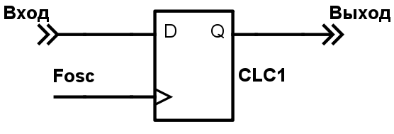
Fig. 6a. Shaper delayed signal.
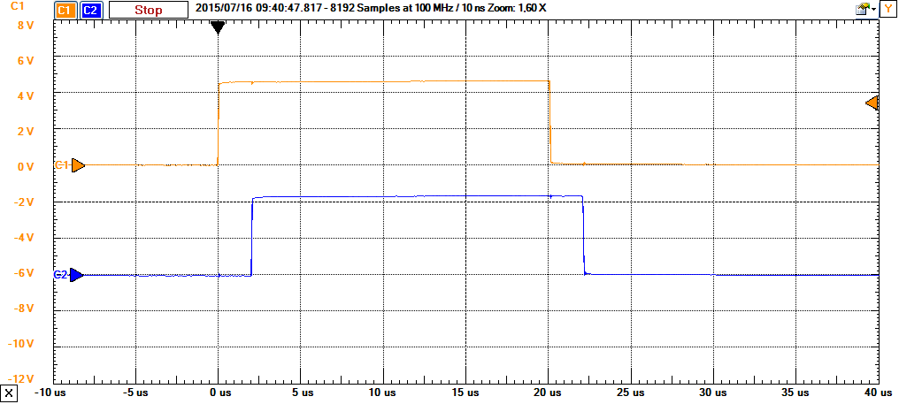
Fig. 6b. Diagrams on the input and output of the delayed shaper.
On the basis of this scheme, it is easy to implement a pulse shaper by changing the state of the input, by the front and by the decay.
Formation of impulses on the front and decline
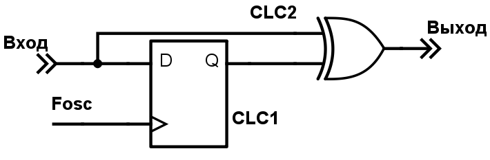
Fig. 7a. Shaper pulse on the front and the decline
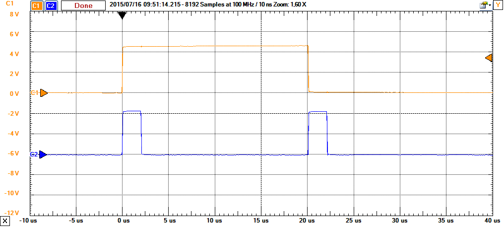
Fig. 7b. Diagrams on the input and output of the pulse shaper on the front and in the decay
Formation of impulses on the front
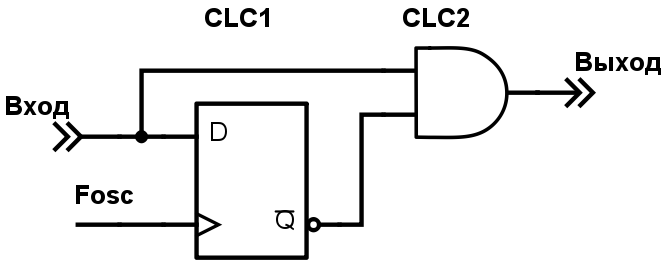
Fig. 8a. Shaper pulse on the front.
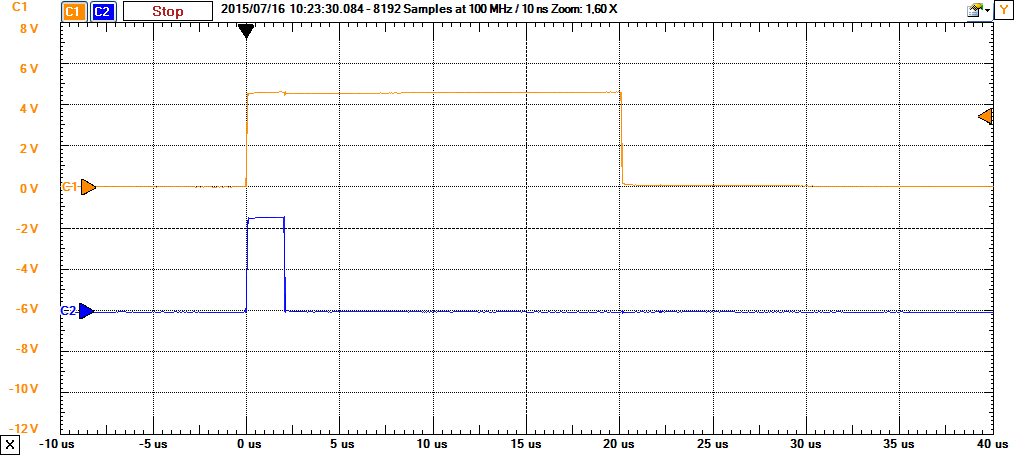
Fig. 8b. Diagrams on the input and output of the pulse former on the front
Formation of impulses by decay
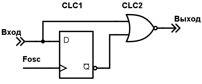
Fig. 9a. Impulse Shaper
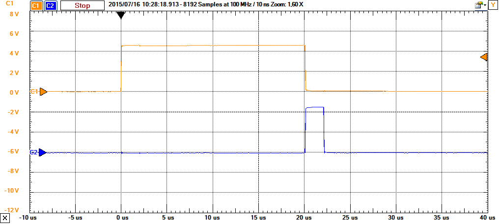
Fig. 9b. Diagrams on the input and output of the pulse shaper by decay
Where can similar schemes be applied?
You can use, for example, when building a pulsed power source for blanking the feedback signal from the comparator during the switching of the power switch (for more details, see below).
Contact bounce suppression
When closing and opening the contacts bounce is observed. Surely, many people have come across this phenomenon when questioning the state of mechanical buttons. Logic cells together with a timer can solve the problem in hardware.
The implementation scheme is exactly the same as for the formation of a delayed pulse, only the period of the clock signal needs to be taken longer. The essence of the method is that the trigger output does not respond to the input if there is no clocking signal, so the circuit does not respond to each input switching.
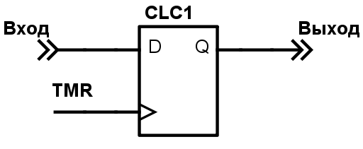
Fig.10a. chatter suppression.
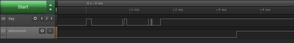
Fig.10b. Diagrams of signals at the input and output of the chatter suppression circuit.
Where does it apply?
Actually poll buttons, preventing multiple false positives.
More options
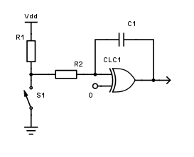
Fig.10c. Delayed chatter with RC-chain
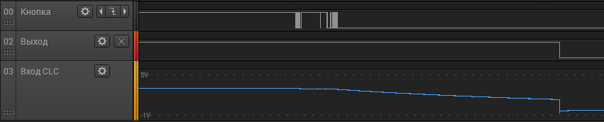
Fig.10d. bounce suppression
Unlike the previous example, the delay is determined by the parameters of the RC circuit and does not require the activation of the timer.
Quadrature encoder
A quadrature encoder is a device that, when its axis rotates, two quadrature signals are formed (out of phase). It is used in determining the speed (angle of rotation or speed) and the direction of rotation / movement. Perhaps the most famous application is the mouse wheel.
Below are two schemes for decoding quadrature encoder signals.
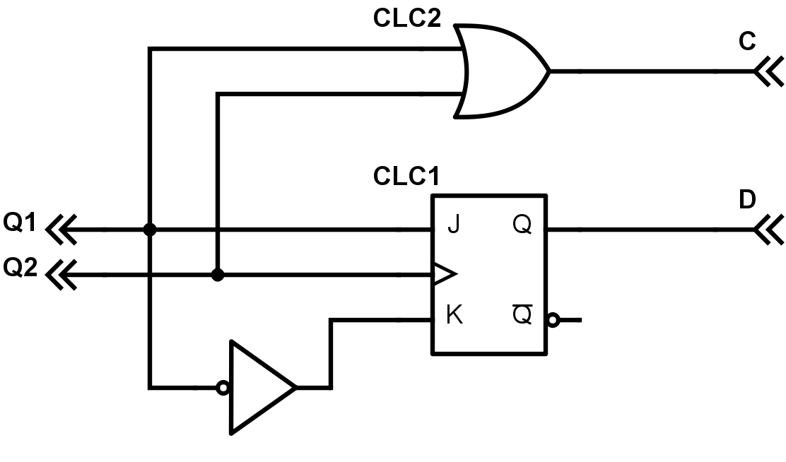
Fig. 11a. Quadrature decoder with counting output and direction signal.
This scheme detects the phases of the input signals (the state of output D indicates the direction of rotation of the encoder) and outputs clock signals (output C).
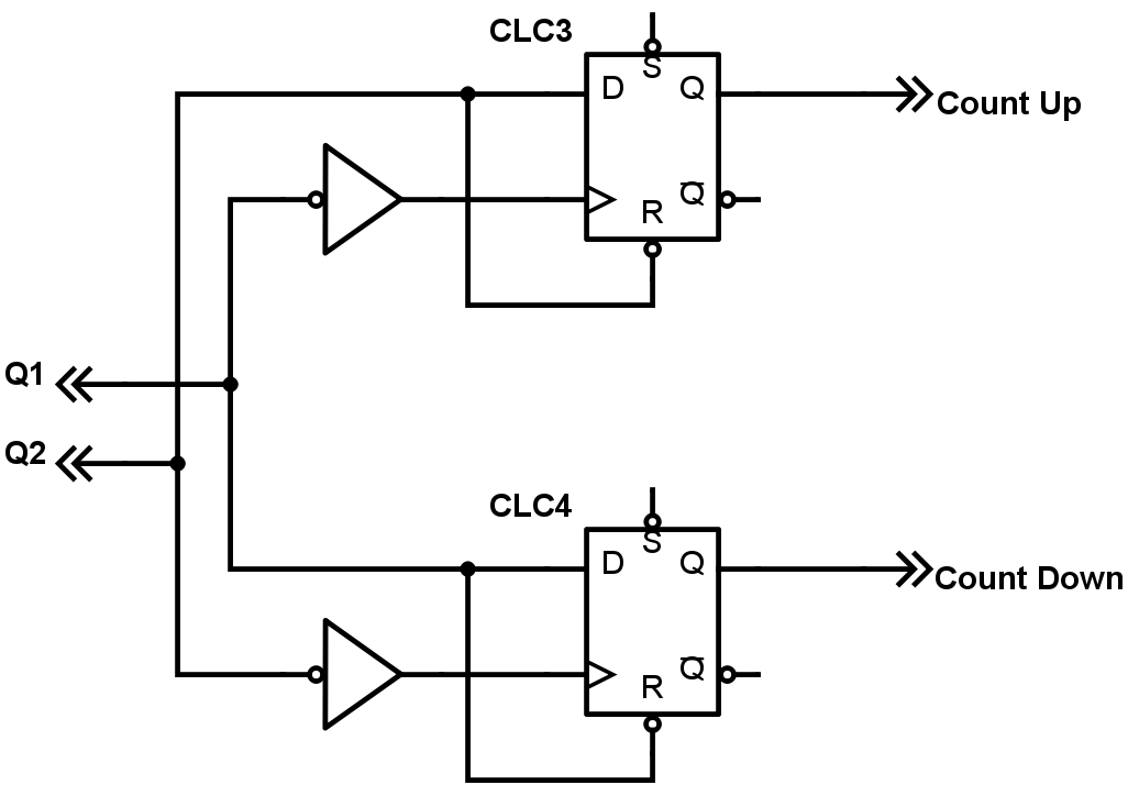
Figure 11b. Quadrature decoder with two counting outputs
This circuit emits pulses. One exit at rotation clockwise, the second exit - at return rotation.
When switching contacts, the encoder generates multiple false positives (contact bounce).
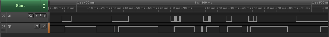
Fig. 11c. Signals from the outputs of a mechanical quadrature encoder
Here is a larger fragment:
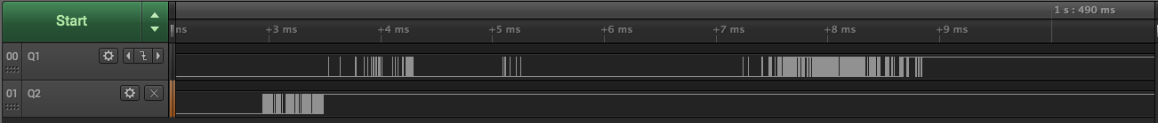
Fig. 11d. Signals from the outputs of a mechanical quadrature encoder
Therefore, both circuits need bounce-free signals. Earlier, we considered hardware chatter suppression options on CLC cells.
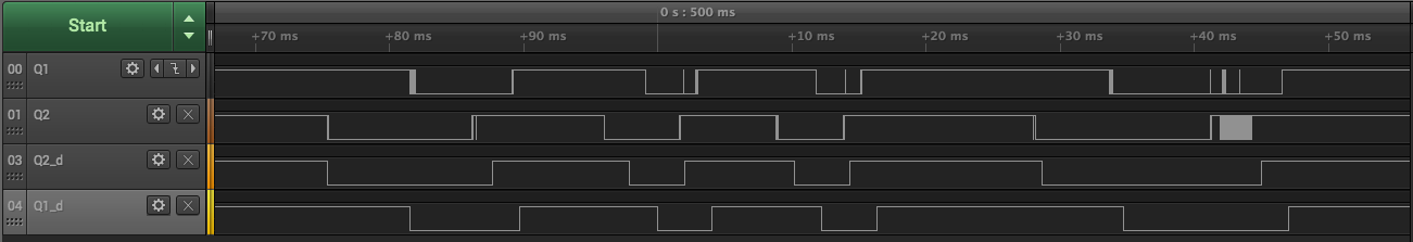
Fig. 11e. Input signals from the encoder and bounce free.
For the processing of quadrature encoder signals, 4 CLC cells will be needed - two for chatter suppression and two for detection.
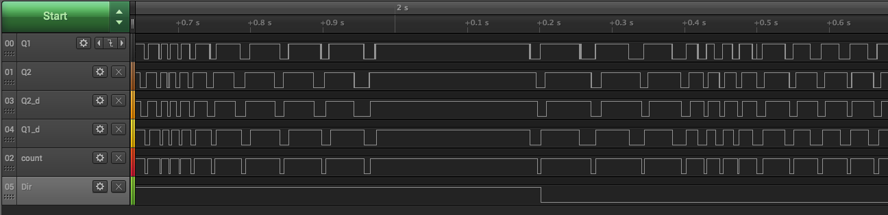
Fig. 11f. Diagrams of quadrature encoder processing signals for a circuit with direction output
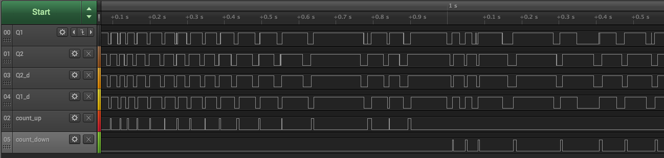
Fig. 11g. Diagrams of quadrature encoder processing signals for a circuit with two counting outputs.
The inputs and outputs of logic cells can be connected to the ports of the microcontroller, and can only have internal connections. For this example, only two inputs are needed, the decoder outputs can be connected to the internal counters of the microcontroller, generate interrupts, interrogate the program, etc. ... But for testing tasks, all CLC outputs can be brought out and the correct operation of the circuit can be checked.
Where does it apply?
Mechanical and optical encoders, counting the number of people entering and leaving, closing the turnstile when passing in the wrong direction))
Manchester Coder
Manchester coding is widely used in signal transmission. Each bit is divided into two intervals, after the first interval (in the middle of the information bit) the signal level changes. The transfer of each information bit is accompanied by a change in the level, Zeros and Units differ in phase (1 - difference from 0 to 1, "0" - from 1 to 0). Thus, the Manchester code has the following features:
- Self-synchronizing - there is no need to transmit special sync signals, since the level of the transmitted signal is guaranteed to change in the middle of the information bit; high information density
- No DC component (signal changes every clock)
The coding scheme is very simple and uses one logical element EXCLUSIVE OR.
At the output we get a coded stream.
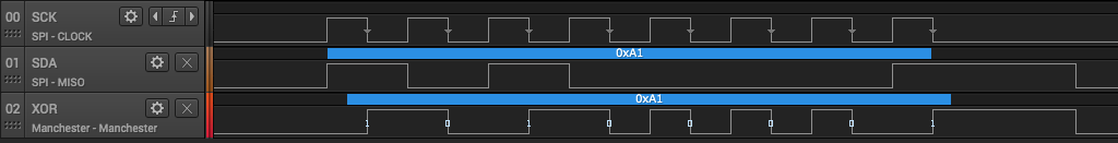
Fig. 12. Diagrams shaper Manchester code
Manchester code decoder
The circuit of the Manchester decoder is much more complicated. Its task is to isolate the sync pulses and bit stream.
In the application example of AN1470 [2], the following implementation of hardware decoding of the Minchester code based on CLC and NCO (controlled oscillator) is proposed.
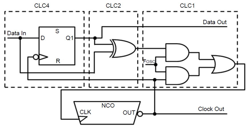
Fig.13a. Manchester code decoder circuit
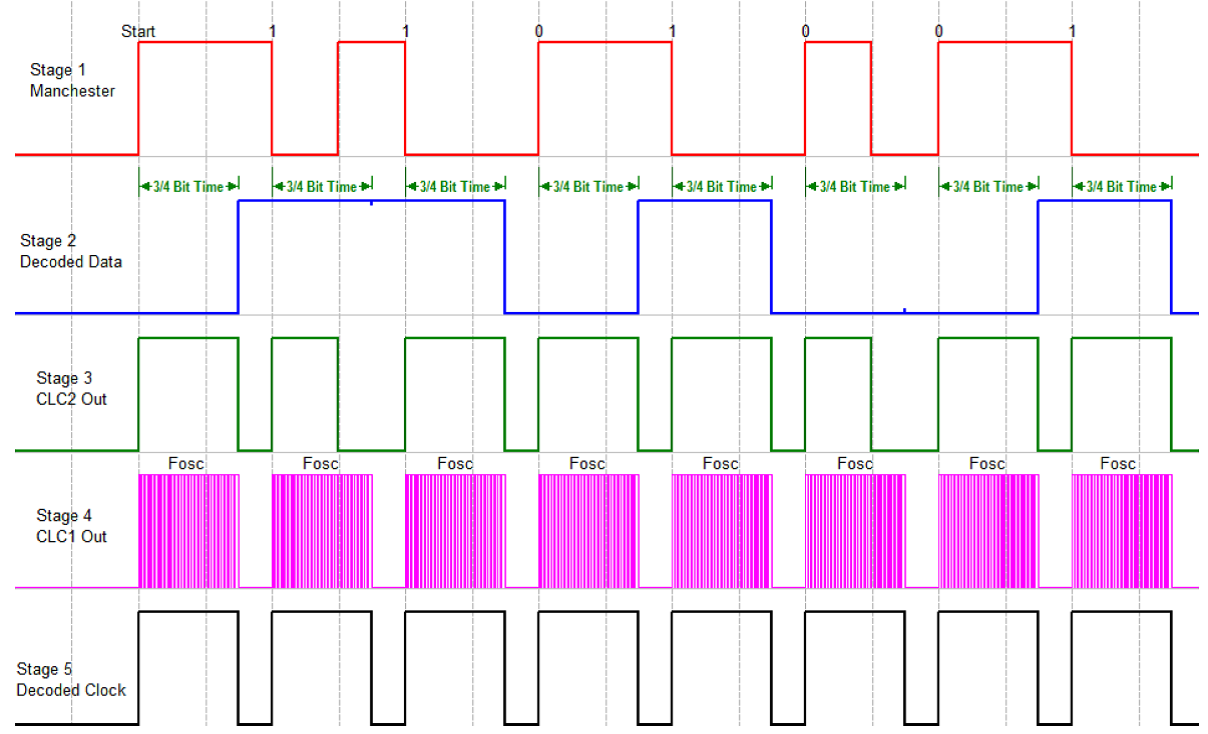
Fig. 13b. Diagrams explaining the operation of the decoder
Stage 1 - D-Trigger
The CLC4 cell (D-flip-flop) latches the input stream on the decay of the synchronization signal. The output from this trigger will be the decoded (recovered) data from the input stream.
Stage 2 - XOR Element (CLC2)
Since in Manchester coding, a change in the signal occurs in the middle of each information bit, it is possible to use the EXCLUSIVE OR element to provide a rising front in stage 3 in the middle of each bit, i.e. we synchronize the decoder in the middle of each bit.
Stage 3 - NCO + AND-OR (CLC1)
NCO module, used to generate ¾ bit interval after which the data is captured (committed). NCO is used in active low state mode. The duration of the pulses can be adjusted using registers. The NCO module needs a source of clock pulses that come from the CLC1.
These two blocks are most important in the decoder. They create pulses of a fixed length after each rising edge of the signal coming out of “stage 2”. The output of the NCO is fed back to the AND-OR element so that if the output from “stage 2” becomes zero, then the NCO will continue to be clocked until it overflows.
Selected synchronization and data signals can be added to the SPI module. Then, after receiving the code send, in the SPI buffer we get the decoded data and receive receive interrupt.
Standby Multivibrator
For the formation of a single pulse on the front or on the fall of the input signal are waiting multivibrators.
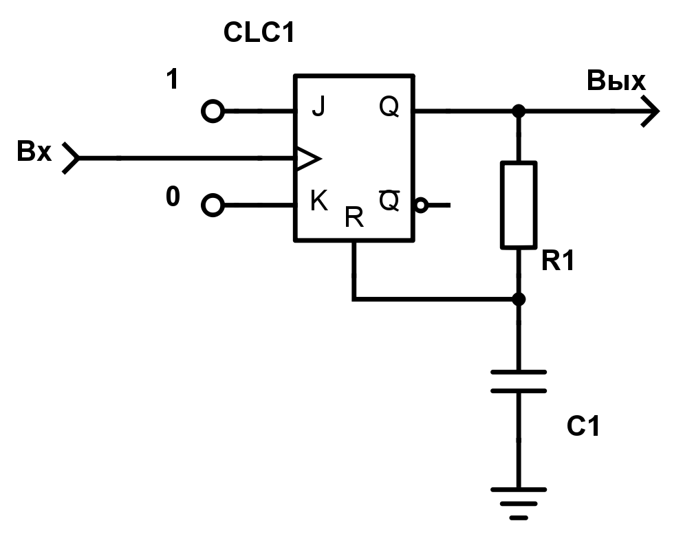
Fig. 14a. The scheme of the waiting multivibrator on the JK-trigger.
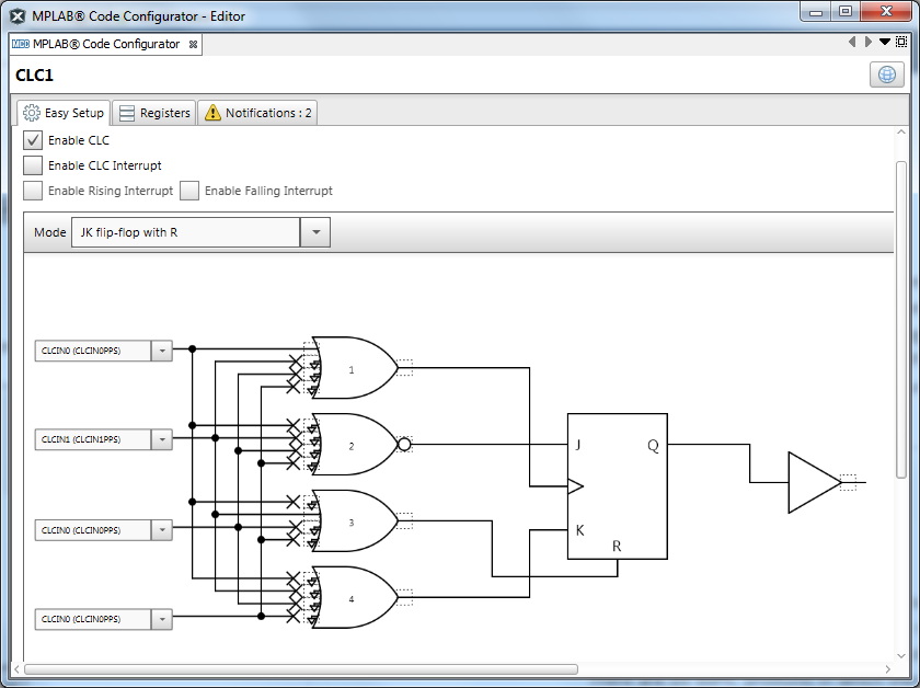
Fig. 14b. The implementation of the waiting multivibrator on the JK-trigger in the PIC-controller.
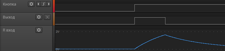
Fig. 14c. Diagrams explaining the work of the waiting multivibrator
Inverting the signal at the synchronization input is implemented by a standby multivibrator with triggering by the decay of the input signal (Fig.14d).
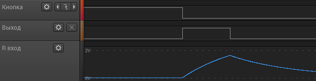
Fig. 14d. Standby multivibrator charts with the launch of the decline.
Unlike the pulse formers considered earlier in the front and in the decay (see Figures 8a, 9a), for this circuit, the pulse duration is not determined by the frequency of the signal at the clock input, but by the parameters of the RC-chain.
Multivibrator
The simplest generator can be made on two CLC (D-flip-flop + inverter).
The disadvantage is low stability, since switching thresholds depend on log.0 and 1 levels of a particular type of microcontroller, which can “walk” on temperature, supply voltage, etc. Besides, it’s not very correct when the digital input signal level is for a long time between 0 and 1.
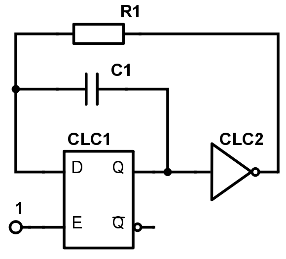
Fig. 15a. The simplest multivibrator on the D-trigger.
The following scheme uses two built-in comparators and one CLC. In this scheme, the thresholds of the comparators are set by the reference voltage source and an external divider (or an integrated DAC). The circuit will be more stable and besides, the comparators have analog inputs and allow any input voltage within the supply voltage.
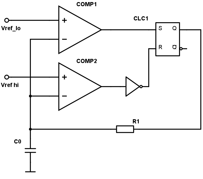
Fig.15b. Multivibrator on two comparators and RS-trigger.
For this example, from the MOT, in addition to the CLC, we will need 2 comparators, as well as sources of reference voltage (external at the divider or internal).
In the initial state, the output level of the trigger is set to log.0, the capacitor is discharged, on the comparator COMP1 output1 appears, the trigger is set to 1, the capacitor is charged through a resistor to the level of the upper threshold voltage (Vref hi), when reaching the input R trigger appears log.1. The trigger is thrown into the opposite state, the capacitor begins to discharge through a resistor, and so on ... Thus, we got a fully software-independent generator. But in this scheme, the microcontroller can programmatically change the frequency by changing the threshold of one of the comparators (changing the reference voltage of the built-in DAC or others).
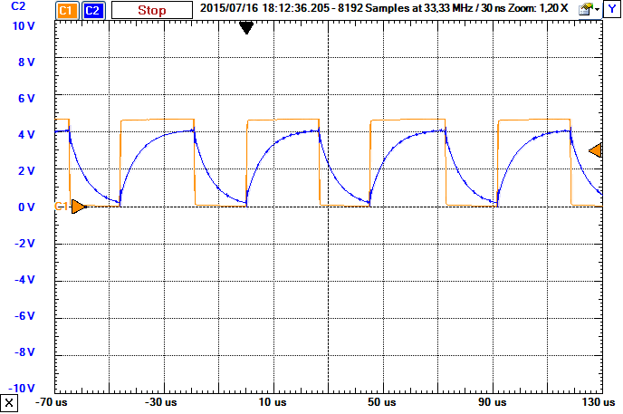
Fig.15c. Multivibrator signal diagrams
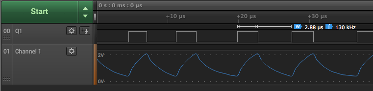
Capacity Measurement. Capacitive sensor. Touch Button
The frequency of the multivibrator (Fig. 15) depends on the value of the capacitor capacitance and the resistance of the resistor. If one of the parameters changes, the frequency changes. Therefore, this scheme allows to measure the resistance or capacitance, for example, using a microcontroller timer.
As a capacitor, a conductive pad can be used, when touched, we will add additional capacitance to the circuit, which will lead to a decrease in the generator frequency.
| signals | comment |
|---|---|
 | Waveforms without touching the sensor |
 | Waveform when the sensor is “pressed” |
Fig.16a. Diagrams of operation of the multivibrator when the time-varying capacity changes.
A similar method can detect water leakage or determine soil moisture and use it to automate flower irrigation))
Switching power supply
Another example of using configurable logic cells in conjunction with embedded comparators.
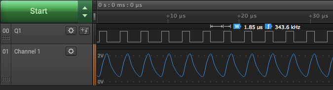
The TMR timer periodically sets the RS flip-flop and opens the power transistor. The current begins to flow through the inductance, the voltage across the resistor R1 increases linearly. When the voltage on R1 reaches the threshold value, the COMP1 comparator is activated and resets the trigger, the transistor closes. The current through the inductance can not be interrupted instantly, so the current begins to flow through the diode D1 and charges the output capacitor. When the timer is triggered, the trigger is set again and the process repeats.
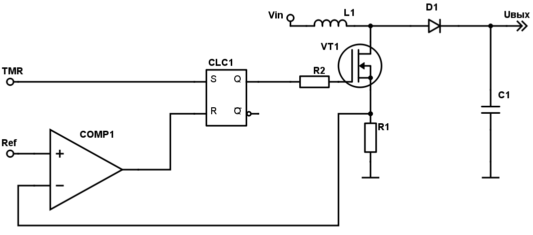
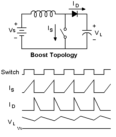
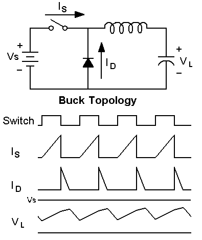
Fig.17a. The simplest switching power supply.
The figure shows a step-up source, but for other topologies (see Fig. 17b), the operation of the circuit will be similar, so I will not draw the output stage.
| scheme | description |
|---|---|
 | boosting |
 | downward |
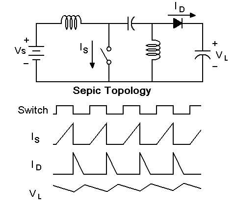 | Sepic |
Figure 17b. Different topologies of switching power supplies
Shown in fig. 17a the circuit performs the function of energy conversion and operates on the peak value of current in inductance. You can also enter the control circuit output voltage. It is easiest to make hysteresis control: when the voltage at the output is below the norm - the source is pumped, when the voltage is higher - the output of control pulses to the power transistor is blocked.
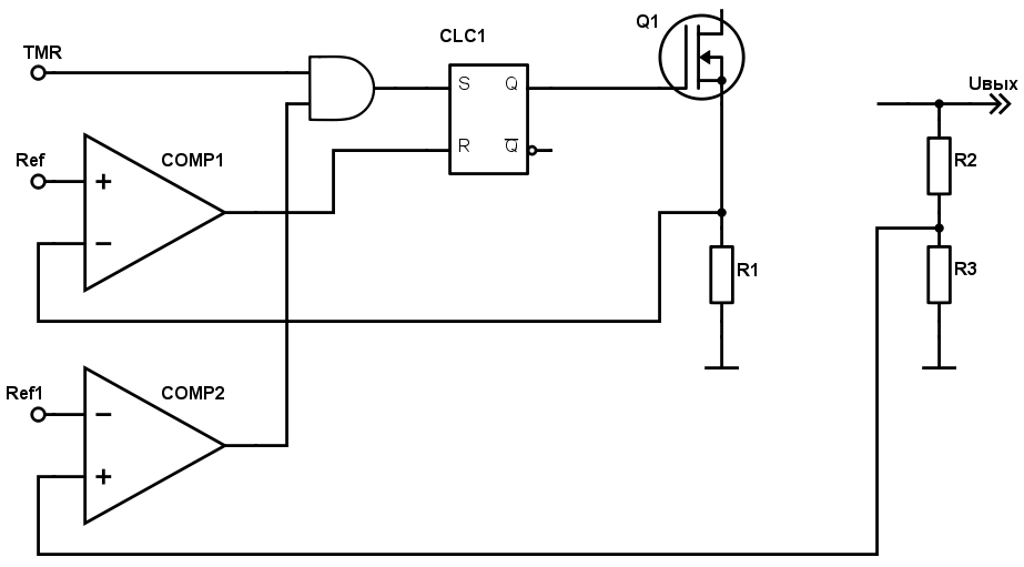
Fig.17c. SMPS with hysteresis control
Turning on the power transistor will generate noise, which can lead to premature operation of the COMP1 comparator. To get rid of this, you can turn on the RC filter in the circuit between R1 and the comparator, or you can add a blocking unit considered earlier (forming a pulse at the front, see figure 8a, or fig. 14a), which, after turning on the transistor, will block the reset of the short time interval
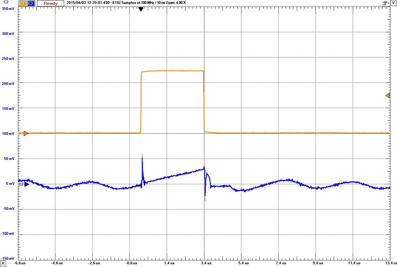
Fig.17d. Interference when switching power key
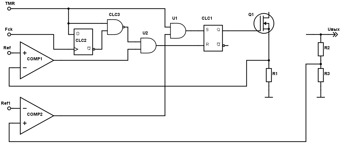
Fig.17e. SMPS with hysteresis control and blanking interference switch.
U1 U2 CLC1, CLC ( Microchip 4 ).
– , . Ref Ref1 . , . . , .
, PIC16F17xx Microchip ( ) : (Slope Compensation) - (Programmable Ramp Generator, PRG), , (COG), HLT . .
, , .. . , – , .
Literature
Continued. 2. /.
')
Source: https://habr.com/ru/post/372509/
All Articles