Useful devices for the home: do-it-yourself WiFi socket
Hello geektimes! In the article I want to provide instructions for creating a WiFi-outlet.
It all started with the fact that in the fall I came across WiFi outlets in stores, I thought it was nothing complicated, then I got acquainted with ESP8266 and realized that I was ready to make an outlet myself.
The socket will consist of:
- Housing;
- ESP8266 12E with power isolation circuit;
- Power supply for ESP8266 from 220 volts;
- 220 volt control board;
- Control panel (button, led, RJ45 port for firmware).
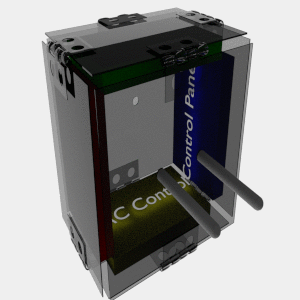
Prototype:
Having broken an article into spoilers, I want to structure knowledge.
The body was designed to be easy to assemble and disassemble during development and debugging, and as transparent as possible to see all the components.
All boards have a maximum size of 5 x 3.5 cm, so the box will be 5 x 5 x 3.5 cm.
Material:
- a piece of plexiglass, the smallest size of 0.5 x 0.25 meters, is enough for a dozen such crafts
- hinges smallest found 2.5 x 2.5 cm
- screws
Plexiglas was cut out with a soldering iron heated to 300 degrees: the cutting line was cut with a knife blade, and then it was run with a soldering iron along the line with pressure on the soldering iron, then held on the other side, and then it could be broken along the fault line.
Holes for screws for hinges drilled a mini drill on the engine with a collet and a 1mm drill.
Implementing a power isolation with ESP8266 on a single board failed due to limitations on the size of the case.
Presented boards are compatible for ESP8266 12F and 12E:
ESP8266 itself relies on this board:

A decoupling of power, and firmware occurs here:

It will take 5 pieces of 10k ohms and 1 piece 470 ohms 0.125 W SMD resistors and 0.1 mkF SMD condenser.
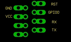
At 6 contacts there are two holes, one for the incoming wire from the Esp8266 board, and the other for the outgoing wire to the board for the RJ45 socket (used for firmware).
PS: The connection "locking on programmator wires" is closed in firmware mode, for example, to make a jumper in the cable with an RJ45 connector.
RJ45 socket board:
Everything will turn out compact.
For power supply, it is easiest to use Chinese USB charging for a phone similar to charging for an iPhone.
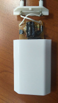
Only the red highlighted zener diode (Zener diode) will be replaced. In USB charging at 5 volts, there is a 5 volt zener diode. To power the ESP8266, you need 3.3 Volts, and a 3.3 Volt zener diode with a power of more than 1 Watt, with a margin judging by the consumption (3.3 Volts, <300 mA).

Next, solder the USB connector and solder to + and -.

It will take:
- 1 pieces 500k ohms and 1 piece 470 ohms, 1 piece 200 ohms 0.125 W SMD resistors;
- 1 Triac
- 1 Opto-pair, MOC3052
- two pairs of terminals for clamping 220 volt wires

The file is available for download along with other resources.
Scripts are here.
I used:
- NodeMcu - needed for running lua scripts
You can get it here https://nodemcu-build.com/ with enduser setup, file, gpio, net, node, rtc-time, sntp, timer, uart, wifi packages.
sudo python esptool.py --port / dev / ttyUSB0 write_flash 0x00000 The_Path_To_The_NodeMCU_Firmware.bin
- Esplorer - to download lua scripts, html, js, css, and other files on ESP8266
https://esp8266.ru/esplorer/ >
To optimize the memory so that the ESP8266 memory, which is not enough, was not spent on compilation, after uploading files to ESP8266, you need to compile .lua files (except init.lua) into .lc directly to ESP8266 via Esplorer.
node.compile ("actionsprocess.lua")
node.compile ("constants.lua")
node.compile ("espgetstatehtml.lua")
node.compile ("estbehaviour.lua")
node.compile ("httpfilesender.lua")
node.compile ("httpsend.lua")
node.compile ("httpsender.lua")
node.compile ("schedulermanager.lua")
I got this
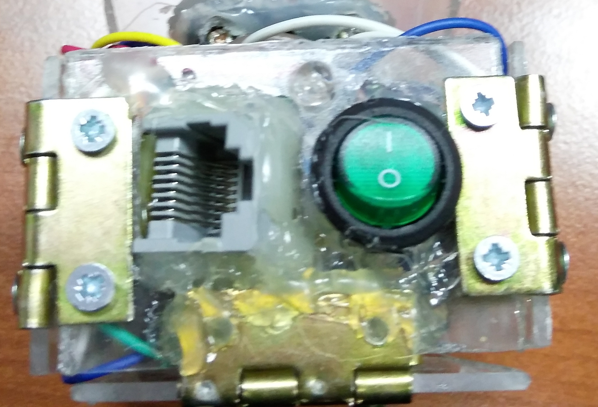
The button switches the ESP8266 to the creation mode of its access point in the “Off” position (to indicate the user Access Point and password to the user access point), and the On / Off state is operational.
LED - lit when the "Off" button (ESP8266 is in the mode of creating its own access point);
- flashes when the On button and ESP8266 are in the process of connecting;
- It does not light when the On button is on, and ESP8266 is connected to the router.
RJ45 socket - for firmware, or power supply via USB Uart adapter.
Control of the outlet comes from the android phone. WiFi Switcher Git-Hub


When the socket and the phone are connected to the router, the android phone sends UDP broadcasts to the router on port 33248, open on the socket. She answers it, sends her Id and Type.


Links
→ ESP8266 - connection and firmware upgrade
→ Lua programming language information
→ Flashing the NodeMCU firmware
→ Rosa tinning of the PCB
')
Source: https://habr.com/ru/post/370093/
All Articles