Toshiba Unveils Low-Power Neuromorph Processor
The Japanese company Toshiba announced its contribution to the development of the Internet of things and the analysis of big data. This time, she developed a very low-power neuromorphic processor for time-delayed neural networks (TDNN). This network consists of a large number of modules that use analog rather than digital processing.
Algorithms for deep learning require a huge number of calculations. They perform on processors with high performance, which consume a lot of energy. However, if we want these algorithms to work on the Internet of things, various sensors and smartphones, we need energy-efficient chips that can perform a large number of operations while consuming very little energy.
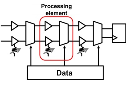
The Toshiba chip uses analog time interval and mixed signal processing (TDAMS) methods. They allow to reduce the size of the neuromorphic processor. Arithmetic operations like addition are effectively performed in TDAMS with the help of a time delay of a digital signal that transmits a logic element as an analog signal. Using this technique, a processor for in-depth study is constructed from only three logical elements and one-bit memory with a fully spatially deployed architecture. A Japanese company created a prototype static-memory chip (SRAM) that successfully recognized handwritten text. The energy consumption per operation was 20.6 femtojoules, which is equivalent to 46 trillion operations per second with 1W of power consumption. The result was 1/6 times better than the last achievement demonstrated at the International Solid-State Circuits Conference 2016.
')
In the von Neumann computer architecture, most of the energy is consumed when data is moved between the memory and the processor. The most effective alternative way to reduce the “path” of data transfer is to put a huge number of processors, each of which will process only one element of the data set, which is nearby. When the input signal is converted to output, a certain weight is assigned to the data storage points. It is the weight that is the parameter that will automatically manage the deep learning process. The closer the point is to the output signal, the greater the weight.
The architecture has similarities with the human brain: the strength of the connection between neurons is the weighting factor that is built into the synapses (processors). Synaptic connections between neurons have different strengths. This bond strength is determined by the output signal. Thus, the synapse performs a kind of processing. This architecture is attractive to developers, but it has one major drawback: its mass production requires a large number of arithmetic circuits that quickly become too large.
Of course, this is not the first neuromorphic processor that can be used in working with artificial neural networks. Companies Qualcomm, IBM, Human Brain Project, KnuEdge Inc. and others are actively engaged in the development of chips that mimic the work of the human brain. In 2014, IBM Research unveiled the TrueNorth chip consisting of a million digital neurons and 256 million synapses that are part of 4,096 synaptic nuclei. Above this development, six years worked for the company employees commissioned by DARPA. They were not in vain: in 2011, the prototype consisted of only 256 neurons, and within three years it counted a million. At the demonstration of opportunities, the chip recognized cars, cyclists and pedestrians in a video from the intersection. An ordinary laptop coped with this task, processing frames 100 times slower and consuming 1000 times more power than the IBM chip. Since 2016, chips have been tested at the Livermore National Laboratory. Researchers are trying to figure out in which area they will be most effective.
Qualcomm introduced its prototype processor that mimics the properties of the human brain, a year before IBM - in 2013. The project was named Zeroth (“zero”). The creators have stated that their processor, located in smartphones, computers, robots and other devices, will allow them to learn in the process. The first chips were supposed to appear in 2014, but this did not happen. Instead, the company released in 2015 the same recognition and computing platform.
Another example is the KnuEdge Inc KnuPath Hermosa processor: 256 processor cores, 64 programmable DMA modules, 72 MB of internal memory, 34 watts of power consumption. The processor consists of 16 bidirectional input-output channels, which allows to ensure the throughput of the RAM subsystem up to 320 Gbit / s. Now the company is actively working to create software that is compatible with the neuromorphic processor. She has already released KnuVerse, which can recognize and identify voice. Unlike other voice assistants, KnuVerse can work in noisy environments. In addition, the developers of the program have solved many security problems. The development was released five years ago, but was used only by the military.
As for the practical application of neuromorphic technologies, Samsung uses the FinFET Exynos 8890 chip in its Galaxy S7 and S7 Edge smartphones. Its main feature is the M1 core, which has a neural network embedded in it .
Source: https://habr.com/ru/post/369857/
All Articles