The University of Berkeley created a nanometer-sized transistor

A group of physicists from the Lawrence Berkeley National Laboratory created the world's first transistor, the size of the gate which is only one nanometer. This is an order of magnitude smaller than the size of the gates of the smallest in size modern transistors.
“We managed to create the smallest transistors to date. The size of the gate is one of the main factors determining the size of the transistor itself. We have achieved a drastic reduction in the size of the shutter, proving the possibility of further miniaturization of electronics, ” says Ali Javey from the University of California at Berkeley (USA).
It is believed that due to quantum limitations, the size of the gate of the silicon transistor can not be less than 5 nm. If you try to make the gate smaller, then the tunneling effect will have a negative effect on the operation of the element. In this case, the transistor stops performing its functions due to leakage currents and other problems.
The manufacturers of electronic devices have not yet reached the limit of 5 nm. Now the minimum size of the transistor gate is 20 nanometers. But scientists, as we see, have already proved the possibility of overcoming the limit of 5 nanometers. In order to circumvent the restriction on silicon, to create miniature electronic elements, experts decided to use other materials: molybdenum disulfide, graphene, or carbon tubes.
')
Scientists from Berkeley were able to combine molybdenum disulfide (MoS 2 ) and carbon nanotubes into a single system. This combination has significantly reduced the size of the shutter. The smallest transistor in the world consists of three main layers. This is a silicon substrate, a zirconia plate, a carbon tube passing through this material, and a film of molybdenum disulfide. The film connects the source and drain of the transistor. Like silicon, molybdenum disulfide has a lattice crystal structure. But electrons passing through MoS 2 are heavier than in silicon. This means that electrons are better retained by the energy barrier of the gate.
Scientists say that molybdenum disulfide forms sheets with a thickness of 0.65 nm with a low dielectric constant value. For this reason, small transistor gates will be able to produce an electric field strong enough to prevent the appearance of a tunnel effect. Unfortunately, miniature transistors created in Berkeley are a piece of work, they cannot be massively produced yet.
“Having created a transistor, we proved that a gate smaller than 5 nm is quite an achievable goal. This limitation proved to be surmountable. And Moore's law can continue to operate, provided that we choose the right materials, ”Javi said. If experts learn to create such transistors on an industrial scale, then in the near future, Moore's law will indeed continue to operate.
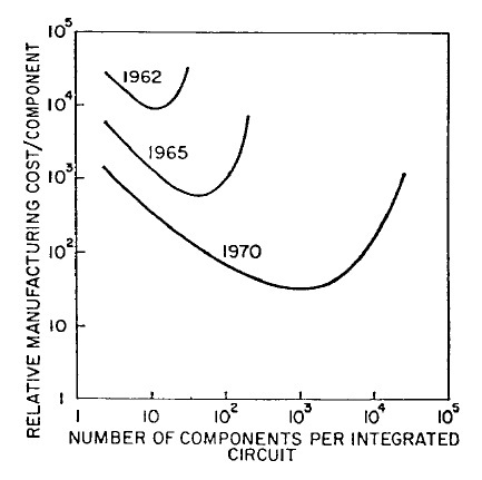
Moore's law was derived by Gordon Moore based on the results of empirical observation. According to the law, the number of transistors placed on an integrated circuit chip doubles every 24 months. This “law” has been known for more than half a century. Actually, this is not a law, but its provisions, in general, are fair.
Representatives of the Semiconductor Industry Association (Semiconductor Industry Association) this spring published a study, according to which in the next six years, Moore's law will cease to operate. The reason is the maximum size of the transistor gates, as described above. One of the proposed alternatives is the creation of 3D-chips with a vertical arrangement of cores, rather than horizontal ones. True, in this case there is another important problem - it is the overheating of the chips. With a volumetric design, the chips will heat up much more, and in this case, in all systems with electronic components with a vertical arrangement of cores, liquid cooling will be required.
Some experts believe that Moore's law is not being carried out with the accuracy attributed to him. It may well be that he is known only because of Intel and its marketing policy. However, now it is more than marketing, since many technology companies are paying attention to a pattern called the law, which has been determining the pace of development of the semiconductor industry for a long time.
Since its inception, several interpretations of Moore's law have appeared:
- microprocessor performance doubles every two years;
- the density of transistors on a chip doubles every 18 months;
- chips of the same type are twice as cheap every 18 months;
- PC performance (computational power) increases every 18 months;
- The number of transistors in new chips doubles every two years.
The results of the work of scientists were published on October 7 in the journal Science.
Source: https://habr.com/ru/post/369753/
All Articles