Intel Wins This Year's IEEE Corporate Innovation Award
The Institute of Electrical and Electronics Engineers (IEEE) announced that Intel will be the next winner of its prestigious Corporate Innovation Award. The award will be awarded for the development and introduction into mass production of innovative technologies of high-k metal gate and tri-gate in Intel processors.
The Corporate Innovation Award was established by the IEEE in 1985. It is awarded to companies or organizations "for outstanding innovation achievements" in the field of activity of the IEEE Institute. At various times, Apple Computer became its laureates for the release of the first mass personal computer, the Jet Propulsion Laboratory for developments in unmanned space flights, Toyota for the invention of the hybrid transmission, and SanDisk as the creator of flash memory.
Under the cat you will find a brief history of the inventions of Intel, who were honored with a high award.
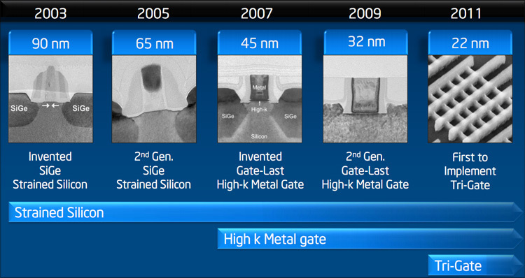
Every year, reducing the technological process of manufacturing processors, by 2007, Intel has reached the threshold of 45 nm. Further, it was necessary to deal not only with production difficulties but also with obstacles related to the physical properties of the materials used. The problem was in the gate dielectric. As the process decreased, the layer of silicon dioxide used as an insulator reached a thickness of only 5 atoms. Further refinement would lead to leaks through this layer, which, in turn, would cause an increase in losses and an increase in energy consumption. The question arose how much further movement forward was justified. Moore's law was under threat.
The problem was known in advance, its solution has been sought by industry leaders since the mid-nineties. Intel was the first to succeed in this; it proposed using hafnium metal-based material as the gate dielectric - its dielectric constant was higher than that of silicon dioxide. The technology was called high-k, where k is precisely the dielectric constant. However, the solution of one problem gave rise to another. A metallic dielectric required fundamentally new gate electrodes; old ones made of polycrystalline silicon were not suitable here. The development of the high-k metal gate technology required an incredible effort of engineers, and the breakthrough history turned out to be so fascinating that its presentation reached the final of the Pulitzer Journalist Prize.
')
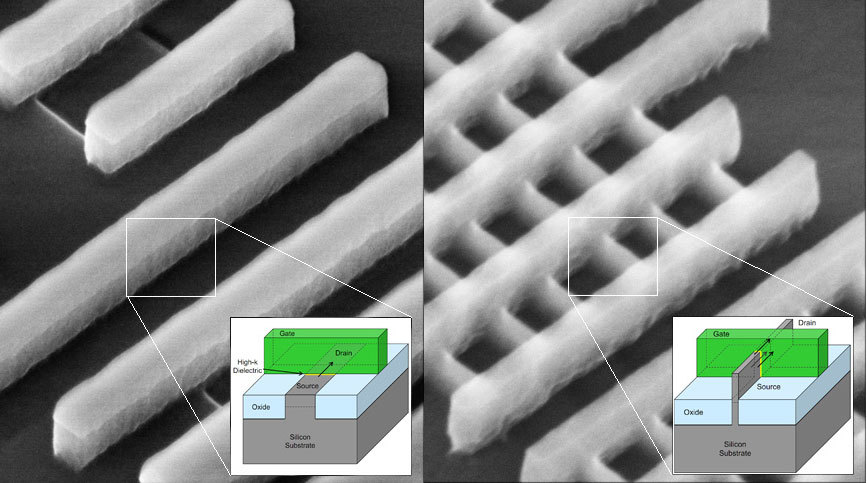
Tri-Gate technology or FinFET was the result of Intel research aimed at reducing leakage in transistors. In the traditional planar structure of the transistor, the electric current can flow only along the narrow surface of the conductor under the gate. While in three-dimensional transistors, the current propagates in the thickness of a silicon ledge, "cutting through" the gate. The result of this design decision is to reduce the resistance of the transistor in the open state, increase the resistance in the closed state and more quickly switch between these states. At the same time, it became possible to reduce the operating voltage and reduce leakage currents. As a result - a new level of energy efficiency and a solid performance increase in comparison with existing analogues. The difference between traditional and Tri-Gate transistors can be clearly seen in the figure below.
The IEEE Prize is the recognition of Intel's merit in solving the most complex problems of microelectronics. Of course, one should not think that all the breakthroughs have already been accomplished - in the laboratories of Intel and at the present time work is underway on the technologies of tomorrow. Those who receive their awards in the future.
Source: https://habr.com/ru/post/369161/
All Articles