Start of development on Kinetis microcontrollers. Fast start

We continue the development of Kinetis microcontrollers. This time we will master the KDS development environment and program the output of the meander. Find out how much time it takes. Find out what the maximum frequency of the meander can achieve and find the amazing speed of Kinetis ports. And of course we will write the classic “Hello, world!” With output via UART at a speed of 1.5 Mbit / s.
Previous articles:
- Microcontrollers of the Kinetis family from NXP-Freescale for embedded electronics
- Open design universal microcontroller module
- Smart board for managing power 3-phase loads
')
Let me remind you that my choice of Kinetis microcontrollers was mainly due to the more advanced software and instrumental support from the manufacturer of these chips as compared to competing solutions. In my professional activity, I had to use many different microcontroller architectures, including 32-bit microcontrollers: STMicroelectronics (STM32), NXP (LPC), Texas Instruments (OMAP) , so there is something to compare with.
So, the previous become about the smart power board demonstrated the hardware capabilities of Freescale microcontrollers from the Kinetis family. The board can control asynchronous motors, heaters, powerful lighting devices and other loads, and in many cases simplifies the creation of reliable and innovative consumer and industrial devices and installations.
Now you need to tell how to program Kinetis .
Before this, it is desirable to have the experience of programming such microcontrollers. These include any 32-bit microcontrollers made on the ARM Cortex-M3, M4, M7 core. But if before that they had dealt only with Arduino , then it would be more difficult, but also more interesting, because it opens a window into the wide world of efficient, functionally rich embedded systems.
What do we need to start?
1. Board with a microcontroller of the Kinetis family.
2. Debug adapter for connecting a PC to the microcontroller JTAG / SWJ-DP interface
3. Oscilloscope.
4. Integrated IDE development environment adapted for Kinetis microcontrollers
The debug board will be the power board from the previous article .

On the one hand, this board will allow you to immediately implement useful applications without unnecessary soldering, on the other hand, the real quality of the development environment and development technology can be assessed only on non-standard boards like this, since for standard debugging boards everything will work perfectly, but at the same time and not practical.
I would strongly recommend the debug adapter Segger J-Link . And it is the original. This will be a justified investment, even if you are not going to program Kinetis , but, say, are targeting other chips on the ARM core.
Oscilloscope, preferably 4-channel, the board still works with a 3-phase network and with a bandwidth of at least 200 MHz, since the frequency of the output signals of the microcontroller can reach several tens of megahertz.
Installing an integrated development environment
Freescale has developed a free Kinetis Design Studio (KDS) software package for working with Kinetis . This package exists in implementations for Linux, Mac and Windows . It includes an integrated development environment based on Eclipse , GDB debugger , GNU compilation and build tools , a special Processor Expert plug-in for auto-generating Kinetis source files and a plug-in supporting debugging of real-time operating systems MQX and FreeRTOS, and much more to read. on the product page.
You can see that KDS is very different from the competing product STM32 CubeMX in that it is a complete development environment in which not only projects are generated, but also compiled and debugged.
The package may require registration on the Freescale website, but it will not take long.
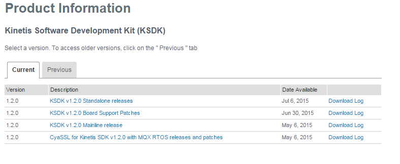
When you find the download page of Kinetis Design Studio you will see the following picture:

Further we will consider only option for Windows .
Download the main package and updates:
• Installer: Kinetis Design Studio installer for Microsoft Windows 3.0.0
• Processor Expert for Kinetis 3.0.1 Update
• Project Wizard support for Kinetis KM14, KM33 and KM34
Sources KDS v3.0.0 Source Files Package download is not required.
Install Kinetis Design Studio installer for Microsoft Windows 3.0.0 .
Downloaded updates install already from the running IDE Kinetis Design Studio (KDS) . Each archive with an update has instructions on how to do this.
In addition to Kinetis Design Studio itself, you also need to download the KSDK v1.2.0 Mainline release software package, which contains: source codes for the peripheral drivers used in Processor Expert , software for hardware abstraction levels, source texts for real-time operating systems (MQX, uCOS-II, uCOS- III, FreeRTOS) , middleware (LwIP, FATfs, RTCS, MFS) , USB stacks, etc.
Here the download page can appear as follows:
Download:
• KSDK v1.2.0 Mainline release and with it the patch Eclipse update patch for Kinetis SDK v1.2.0
• CyaSSL for Kinetis SDK v1.2.0 with MQX RTOS releases and patches
The remaining packages are designed for specific debugging boards and are not interested in us now.
CyaSSL is a useful package that will come in handy in the future.
Install the KSDK v1.2.0 Mainline release and the Eclipse update patch patch for Kinetis SDK v1.2.0.
Here all installations are complete.
This is somewhat longer than an Arduino IDE installation, and may take more than an hour, but the amount of software obtained and the flexibility of solutions is incomparably greater.
The development environment is installed, what to do next to write the first application on Kinetis ?
First of all, remember the exact name of the chip with which we work - this is MK60FN1M0VLQ12 .
Next we need documentation for this particular chip:
• Data sheet
• Reference Guide
Documentation is provided not on a specific chip, but on a subfamily (Sub-Family). Therefore, it will take some effort to search the documentation for the actual configuration for our chip. Reference manuals from different manufacturers vary greatly in style from each other. This is sometimes the strongest obstacle to the transition to a new architecture. The good news is that the Kinetis documentation is one of the most comprehensive and detailed, and the Kinetis microcontroller forum is not inferior in activity to other general electronic forums.
Reference Guide for us the most important document. Freescale manuals have a feature - one of the first chapters under the name Chip Configuration contains short clarifications on the composition, connection and functionality of individual peripheral blocks of the chip. This chapter should be studied without fail when reading the complete descriptions of the peripheral modules contained in the individual chapters of the manual.
The entire manual will probably never be read, it is more than 2,100 pages, but the first 9 chapters are worth a quick glance.
Now run KDS and create an empty project.
 | A dialog box appears indicating the path to the Eclipse workspace. Here we can enter any way convenient to us. |
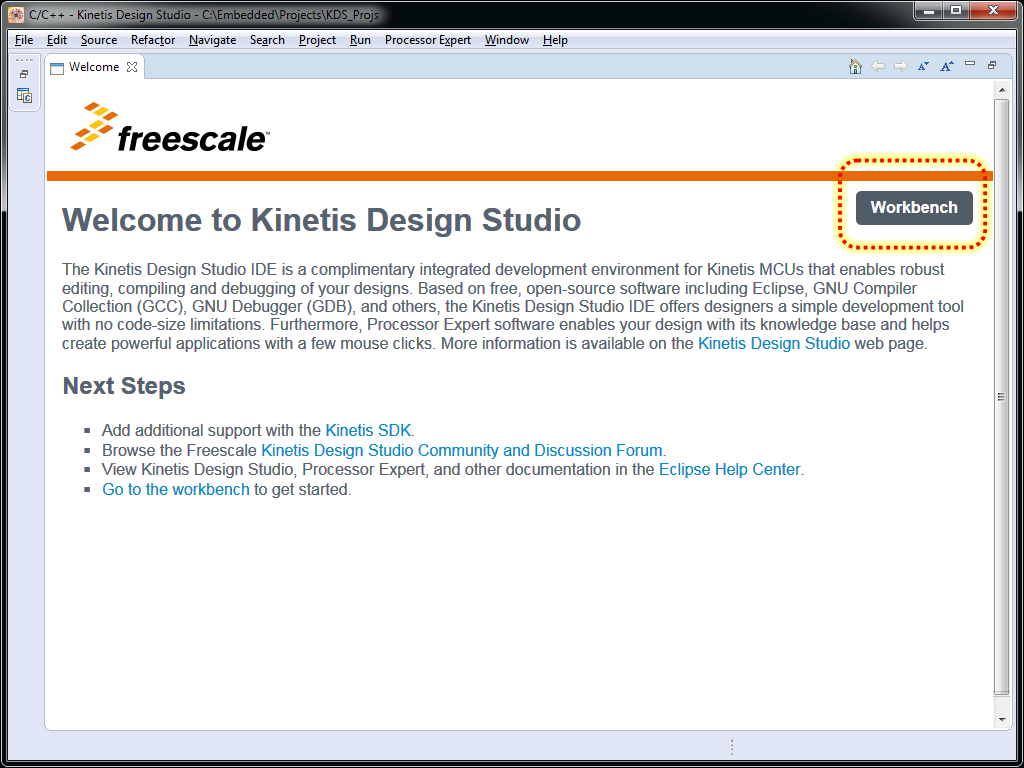 | In this window, do not waste time and press the button in the upper right corner - Workbench |
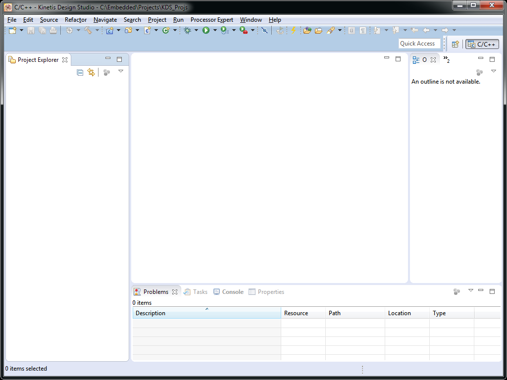 | An empty workspace window opens. Create a project in this space. To do this, select the menu item File-> New-> Kinetis Project as shown below. |
 | Since KDS is based on Eclipse and Eclipse CDT (C / C ++ Development Tooling), there are a lot of items that we don’t need now. Eclipse will continue to suppress the number of obscure features, with this you just have to accept. Then it will all make sense. |
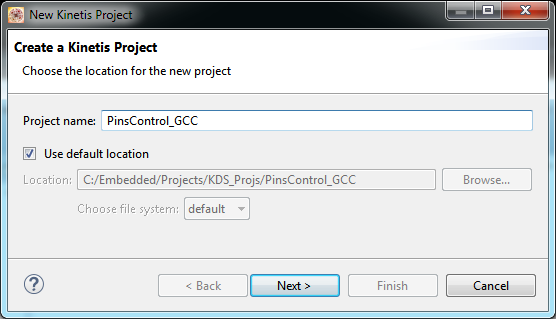 | In the Project Name field we set the name to our first project. In this project, we will program the output of the meander to one of the pins of the microcontroller and find out what maximum frequency we can generate. |
 | In this window, select the chip with which we are going to work. Item Boards for those who decided to still use the debug board from Freescale. |
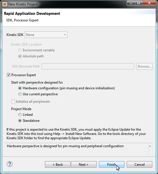 | Here click the Processor Expert checkbox. Select the Eclipse perspective, i.e. the composition and placement of the working panels in the Eclipse window, which, incidentally, can always be changed later. We also decide that we will have a standalone project. will not refer to files somewhere far beyond the project directory, and everything will be copied into the project. Next, click Next. |
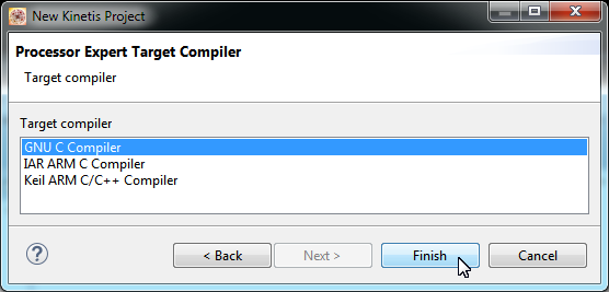 | So far, we don’t know why Keil and IAR want money for their compilers. Choose the free GNU C compiler and finally click Finish. |
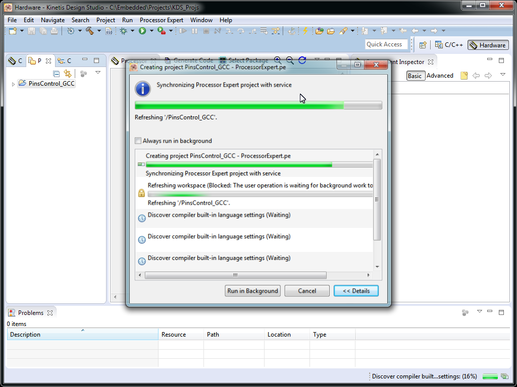 | Work has begun to boil. A lot of files are created in the project directory. Namely, 72 files and 12 subdirectories. |
 | This is what should appear at the end. The blue rectangles on the chip indicate the previously generated initialization of the individual peripheral modules of the chip. Without this necessary initialization, the chip simply will not be able to correctly launch the user program. |
Now we decide on which pin we will generate a signal.
 | On my chosen board, there are special pads for monitoring the OUT1 ... OUT7 signals, as shown in the diagram. Signals are output after ULN2003 (U16) buffer to connector X41. At the microcontroller, these signals are connected to the PTB1-PTB7 lines of port B. We select the OUT1 signal for generating the meander. |
A note about port programming.
Kinetis chips, in contrast to, say, STM32, have two peripheral modules responsible for controlling external external outputs. This is a module called Port Control and Interrupts (PORT) and the General-Purpose Input / Output Module (GPIO).
In the PORT module, rarely changing pin properties are configured, such as assigning an alternative function, assigning an interrupt, output driver strength, connecting pull-up resistors, connecting filters, etc.
In the GPIO module, the output is operatively controlled: setting the signal level, reading the signal, setting the output direction.
We configure peripherals for the meander generation program.
While we are not writing any code, everything is done through dialog boxes and panels in KDS.
We need, first, to configure the clock subsystem, and second, to configure the output port.
Without going into the specifics of the clocking subsystem, which is quite complicated, I’ll just provide screenshots of the dialog panels with the correct settings.
Setting the clock subsystem
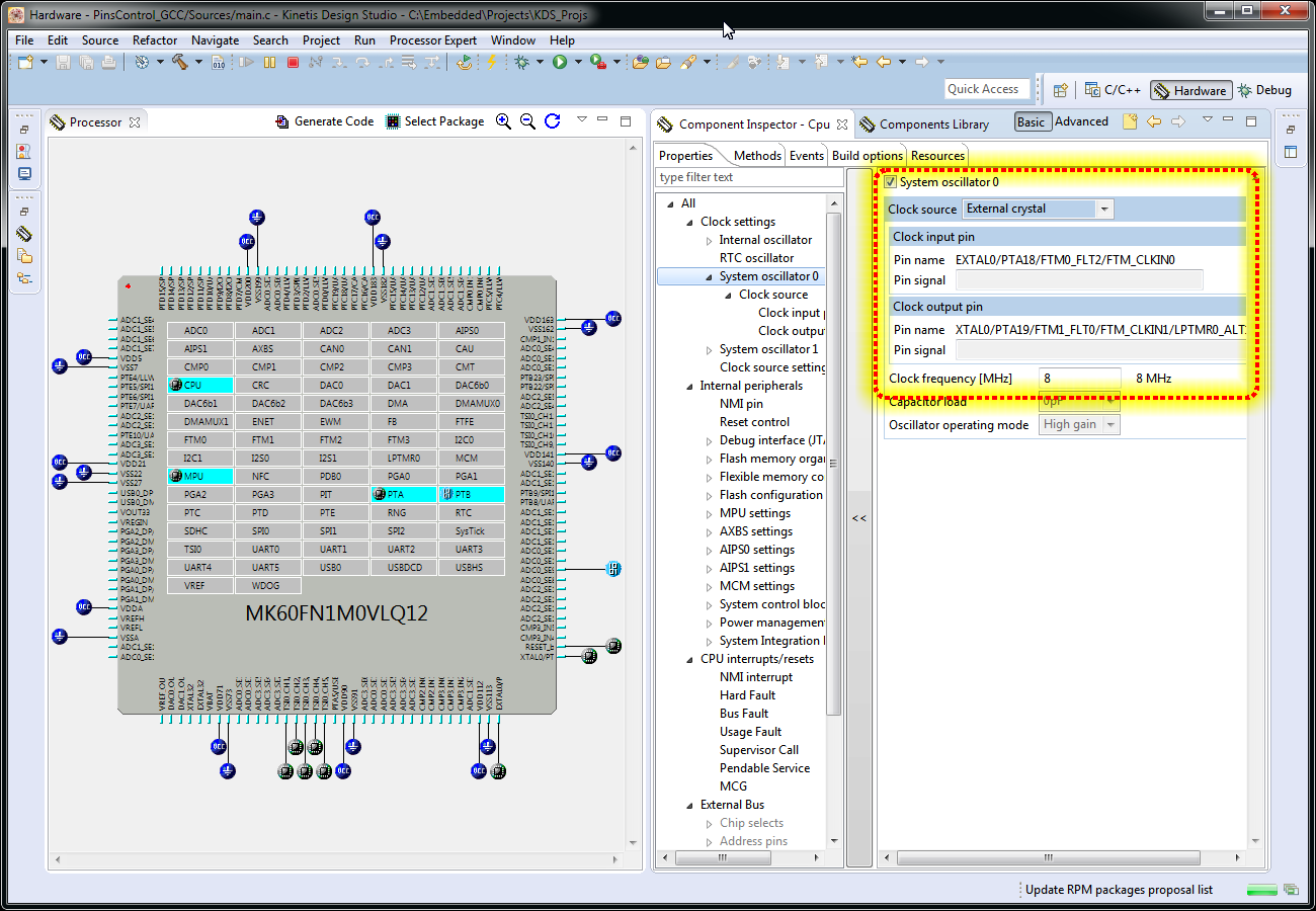
Here we activate the system oscillator 0. Record the frequency of the external quartz and set on which pins the external quartz of the oscillator 0 is connected.
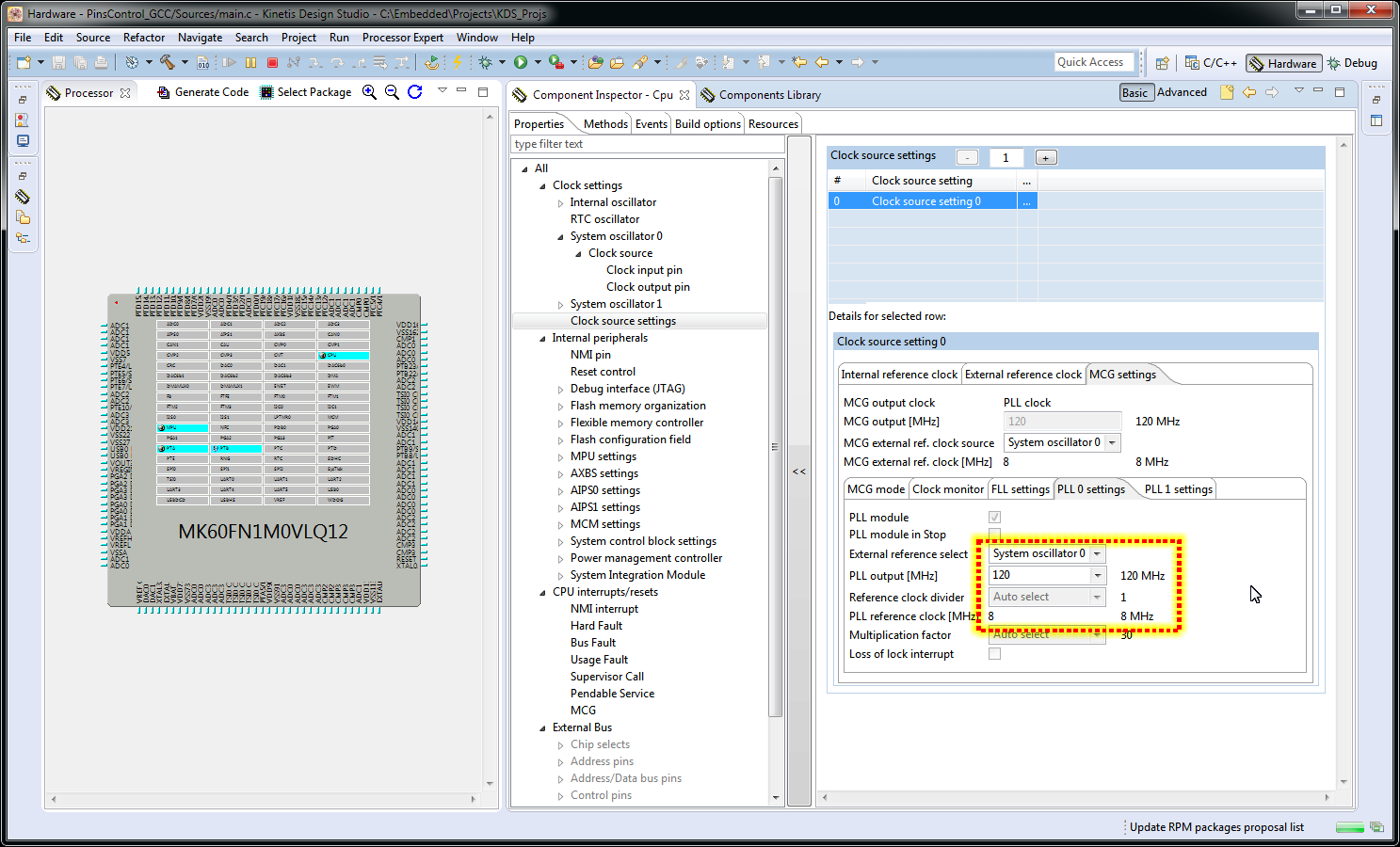
We indicate that the oscillator output 0 is fed to the frequency multiplier 0 (PLL0). A multiplier raises the frequency to 120 MHz.

We use the frequency multiplier 0 (PLL0) to clock the processor. To do this, turn on the PEE mode (see decoding in the manual) from the PLL0 output.

We configure Core Clock, Bus Clock, External Bus Clock, Flash Clock . KDS will not let you enter erroneous options for these settings. The screenshot shows the settings for the maximum possible frequencies of all these signals.
Setting the meander output line
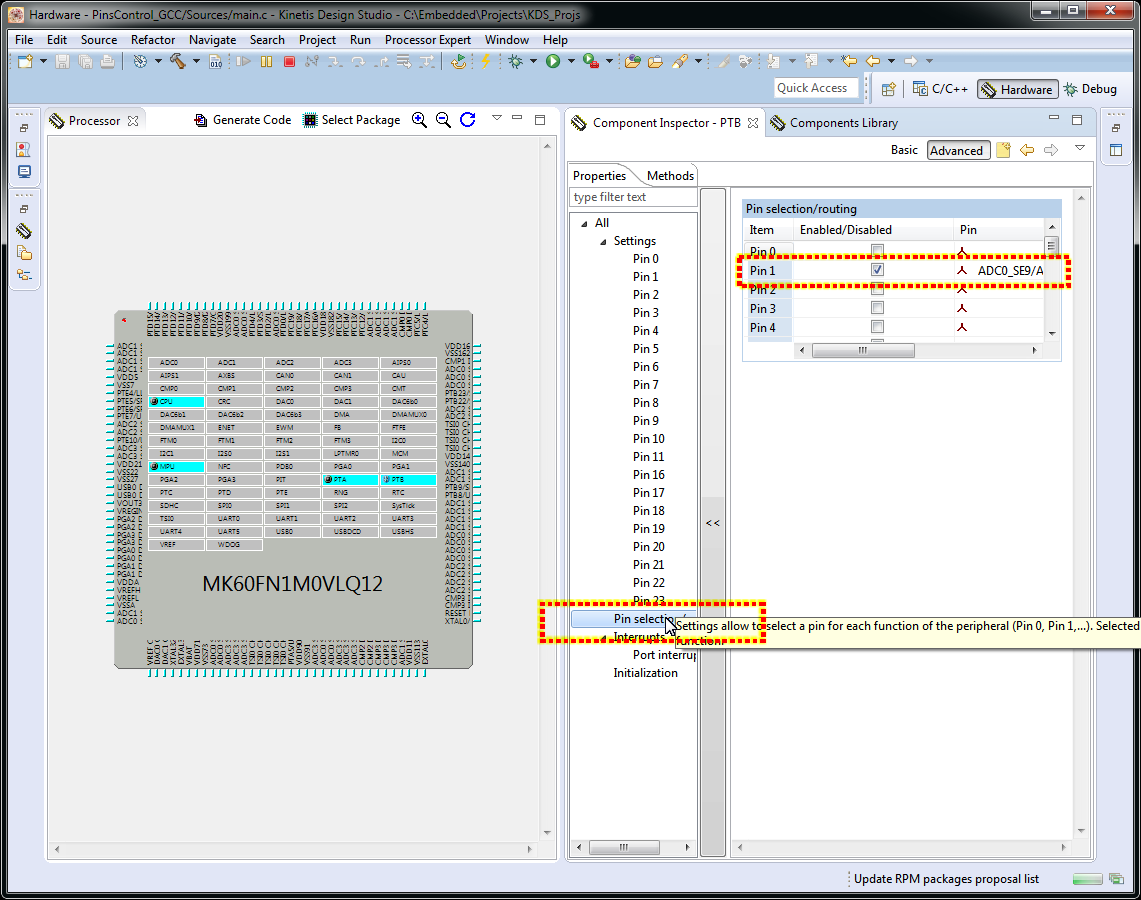
We allow the work of output 1 of port B. This will lead to the generation of initialization of the port at the start of the program.

Configure the mode of operation directly output 1.
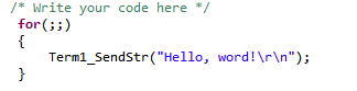
Configuration is complete. We write our program
The program consists of only two lines. This is much less than for similar functionality would have to write on the Arduino .
The program is written to the file main.c already generated in the previous step.
And the program looks like this:
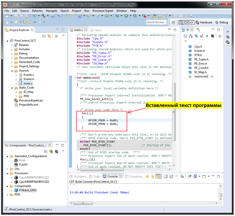
Important to remember.
When generating source files, the main.c file is overwritten. This erases all changes made to it in improper places.
Only a fragment remains intact in the main function, starting from a comment.
/ * Write your code here * /and before comment
/ *** Do not write it over during the code generation. *** /
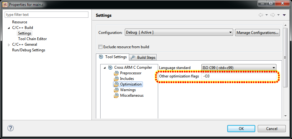
Before compiling the program let's make a couple of important settings.
In the properties of the file main.c called from the context menu of the file we set the maximum level of optimization:
To make the program debugging more convenient in the menu Window-> Preferences -> C / C ++ -> Debug -> EmSys Register View, we indicate the settings as in the screenshot.

Generation, writing to Flash and running the code for execution
Generate code with the Project -> Generate Processoe Expert Code .
Writing code in Flash and starting execution are performed with the command Run -> Debug (F11)
At startup, a dialog should appear asking you to select a debug adapter.
I choose Segger because it is he who is connected to my board.
If the download passed without errors, then after the breakpoint on the function PE_low_level_init (); click Resume and on the screen of the oscilloscope connected to the signal OUT1 on the board should appear here is a picture like this:
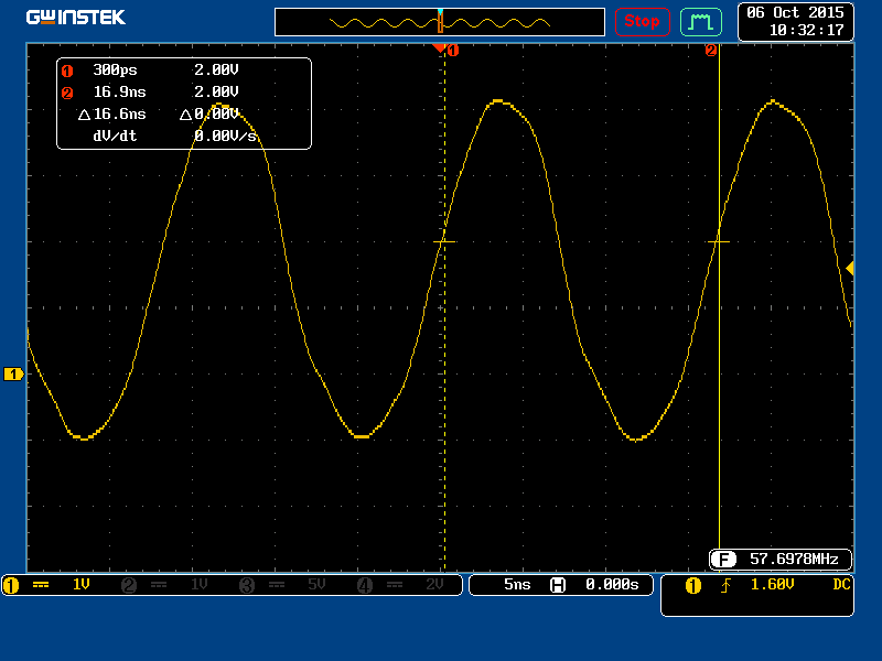
The sinusoidal signal should not be confused.
Since we are dealing here with a 60 MHz meander, a limited probe bandwidth, oscilloscope bandwidth, probe capacitance, reflection of the signal in the conductor between the measurement point and the microcontroller output and the microcontroller output speed begin to have an effect.
However, it can be seen that the microcontroller is capable of generating a frequency of up to 60 MHz , which roughly corresponds to the frequency of the television signal.
It is also interesting that reducing the frequency of the bus in half the frequency on the external output will not change. Those. Microcontroller MK60 always writes to the port in one clock cycle of the core frequency.
Writing "Hello, world!"
Everything is simple here.
Add the Component Term component from the Componrnts Library to the project. And tune it to the speed of 1500000 bps. We also indicate that it will work in the UART5 channel (connector X37) and assign external pins for the Rx and Tx signals.

The text of our program will be as follows:
We tear off the terminal emulator program on the PC and observe the result.
True rare RS232-USB adapter can support this speed.
For this, I recommend using adapters from FTDI .
Total.
Thanks to the Freescale KDS environment, we have created two projects that well reveal the potential of Kinetis chips without spending a couple of hours.
And this is just the beginning.
There are still a lot of noteworthy software tools for these chips that can greatly simplify the lives of developers of embedded systems.
The projects presented here for the KDS environment can be downloaded from the link on GitHub:
github.com/Indemsys/SB200BE/tree/master/PCB_SB200BEv2/DemoProjects
Source: https://habr.com/ru/post/368553/
All Articles