Programming Technology ARM Cortex-M0 +
Here I will talk about a convenient set of tools and the technology of rapid development of simple programs on the S9KEAZN64AMLC microcontroller with a 32- bit 40 MHz ARM Cortex-M0 + core . As a hardware basis, let's take a fee from a previously announced project . The board turned out to be surprisingly tenacious at low temperatures and even surpassed the expectations in this sense.
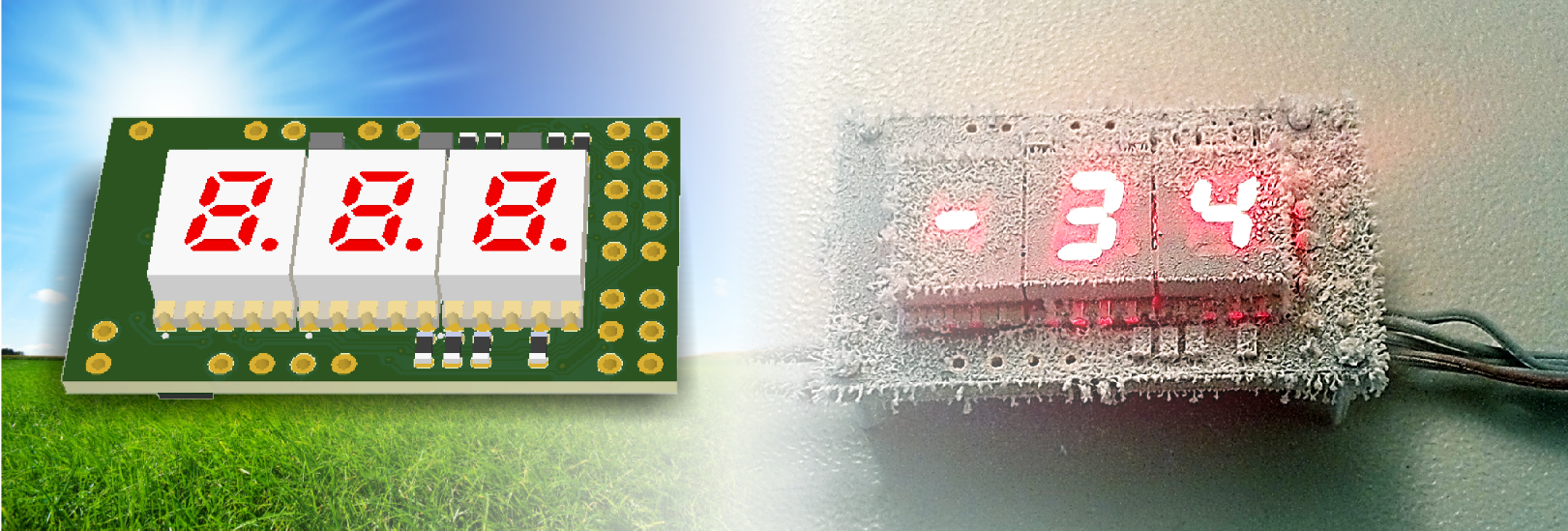
Let's start with a detailed description of the creation of the thermometer without the use of external sensors and with the function of the logger.
Introduction.
As it should be according to the laws of Murphy, the first soldered fresh board burned down. But it allowed to find out that the S9KEAZN64 is able to withstand voltage up to 12 V without breakdown, and the LT3973IDD-5 # PBF stabilizer perfectly tolerates short circuits on the output and maintains a stable output voltage of 5 V at almost zero load. The reason for the failure was the poor soldering of the stabilizer body.
But that was not all! Inattentive study of the documentation led to an erroneous scheme of connecting the two indicator segments to the PTA2 and PTA3 lines of the microcontroller ; they turned out to be conclusions with a clean open collector, i.e. without top key required. They had to be paralleled with the findings of PTB7 , PTB6 and lose the functionality that was previously planned for them. Inattention also led to the absence of a filtering capacitor at the output of the U2 reference voltage source. All this led to small corrections of the board, which I euphonically call tuning .
(Click to enlarge)
')
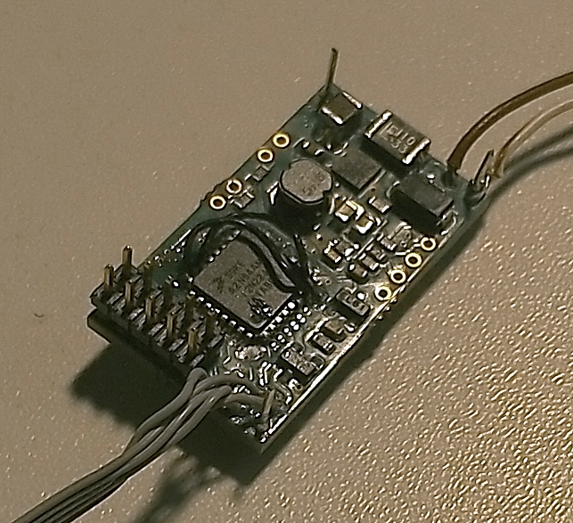
I cite the final version of the board with a microcontroller with a marked tuning.
(Click to enlarge)
Description of the scheme
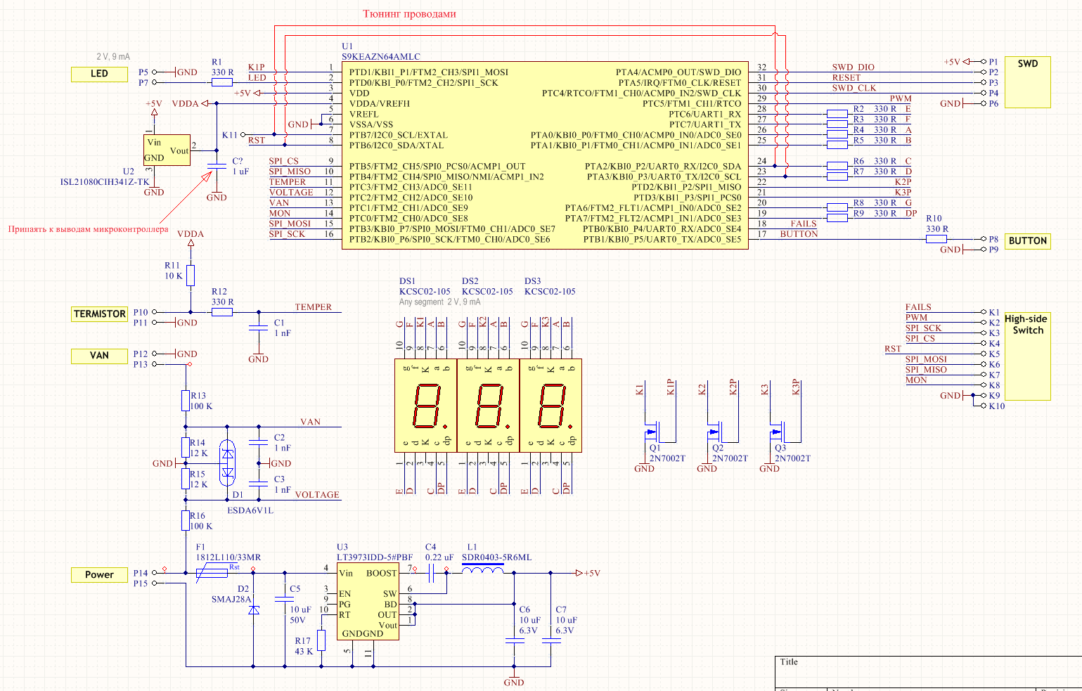
The central element of the circuit is a microcontroller S9KEAZN64AMLC .
Him:
- 32- , - 40 , - , 20 . - FLASH - 64 , - - 4 . - 5 The microcontroller has a multi-channel 12-bit digital-to-analog converter , an analog comparator, two channels of pulse-width modulators, an internal clock generator with a multiplier of up to 40 MHz, a temperature sensor , SPI, I2S, UART interfaces.
The microcontroller can be transferred to deep sleep while maintaining the activity of the ADC and analog comparator.
Digital inputs are additionally protected from interference by the built-in hardware filters of digital signals.
For accurate measurement of analog signals on the board, a U2 reference voltage driver ( ISL21080CIH341Z - TK ) is located with an output voltage of 4.096 V. This is conveniently combined with a 12-bit ADC range of 4096 counts.
The original purpose of the board was to work as a controller for car headlights. Therefore, the original labels of assigning pairs of contacts on the board are left. But of course they can perform other arbitrary functions. I will list these pairs:
LED - Exit. Connecting an external LED. May be the entrance.
TERMISTOR - Login. Connect an external temperature sensor based on a thermistor, but there may be another sensor with variable resistance.
VAN - Login. Voltage measurement from 0 to 30 V
BUTTON - Login. Connect button. It can be an output or analog input.
High - Side switch - a group of signals designed to control the power multichannel key card with SPI interface. In the absence of such a board, the signals remain free for other functions.
The microcontroller according to the specification is capable of operating up to -40 ° C. During the tests, he continued to work at -42 ° C. Lower temperature just could not be obtained.
For the board, the dependence of the maximum current consumption on the supply voltage was measured, with all the LED indicators on.
The normal operation of the board according to this schedule lies in the range from 6 to 30 V. After 30 V, the shunting of the suppressor D2 begins to activate and then the current increases unlimitedly until the suppressor breaks out or the self-resetting fuse F1 of 1.1 A rated continuous current trips.
The board is turned on at a voltage of 3.5 V , but the ADC begins to function normally from 5 V, and the rather low level of noise in the measurements starts from 6 V.

(Click to enlarge)
The next step is to solder the SWD interface
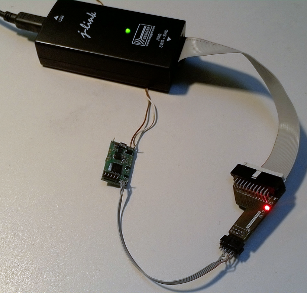
SWD interface is what fundamentally distinguishes programming for ARM from programming 8-bit microcontrollers such as Arduino. With the SWD interface, the program on the microcontroller is also easy to debug as if it is executed locally on your computer. If we add to this the convenience of technology such as a communication channel and real-time debugging RTT , then to return to the 8-bit microcontroller completely disappears from any desire.
In the diagram, the interface is indicated by a rectangle SWD with the contacts P1, P2, P3, P4, P6 located next to it. I use Segger's J-Link SWD adapter. For him, I have adapters for more miniature connectors. I used this adapter here to connect to the board. The power supply in this case comes from the board to the J-Link adapter. The adapter has a two-way power supply buffer converter, so there is no risk of applying 5 - volts to the adapter. How exactly to solder the adapter signals to the board can be found by reading the manual for the adapter. A more economical option would be to use OpenSDA adapters that are present on many cheap debugging boards from NXP-Freescale , but in this case you have to sacrifice some of the J-Link features.
Start programming
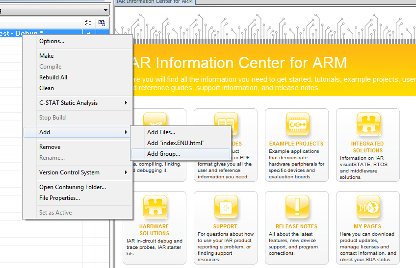
For Kinetis series microcontrollers from the former Freescale company, there is a special Kinetis Design Studio (KDS) development environment . The environment was created with the intention of freeing the developer from in-depth study of programming guides and datasheets. To some extent this turns out. Therefore, we start with KDS . The environment will generate us the source texts of the microcontroller peripheral initialization procedures, the project directory structure and the stub for the main function, insert the necessary header files and the linker configuration. In it, we can also carry out a compilation of the project until we move on to a more efficient tool.
Create a subdirectory Firmware in the project directory. Launch Kinetis Design Studio 3.0.0 IDE and create a workspace in Firmware . Then in the menu File-> New-> Kinetis Project enter the name of the project, say - AccTester . Choose a family of microcontrollers SKEAZN64xxx2
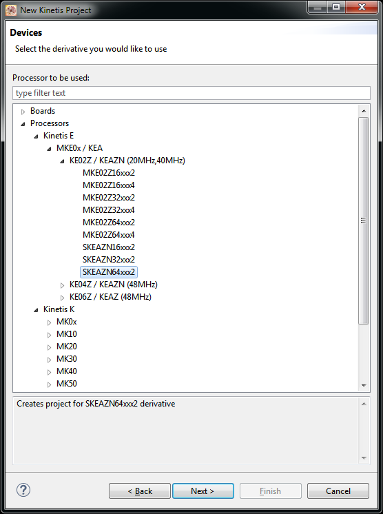
(Click to enlarge)
Then this dialogue:
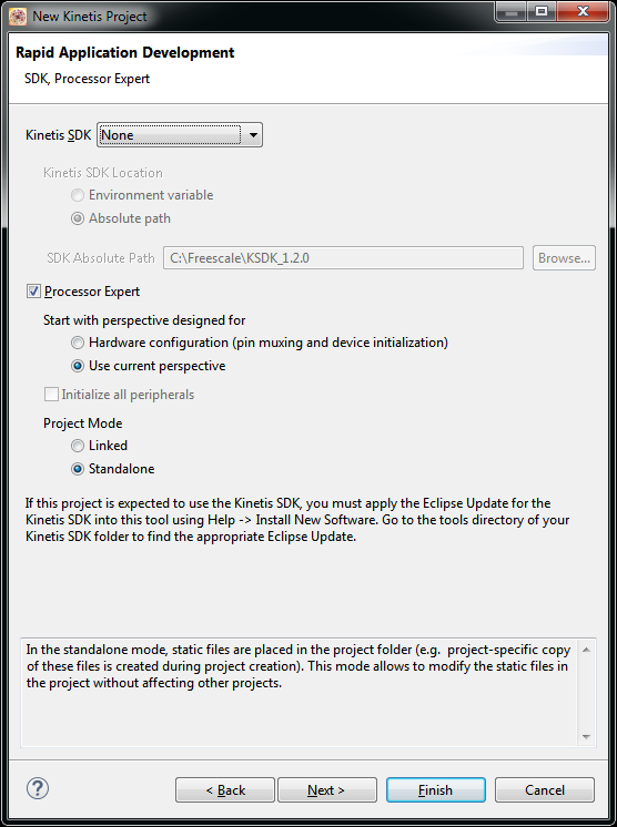
(Click to enlarge)
Then we select the IAR compiler. We can choose GCC , but then the article will be about IAR.
An explanation can be found in this comparison of compilers was carried out here .
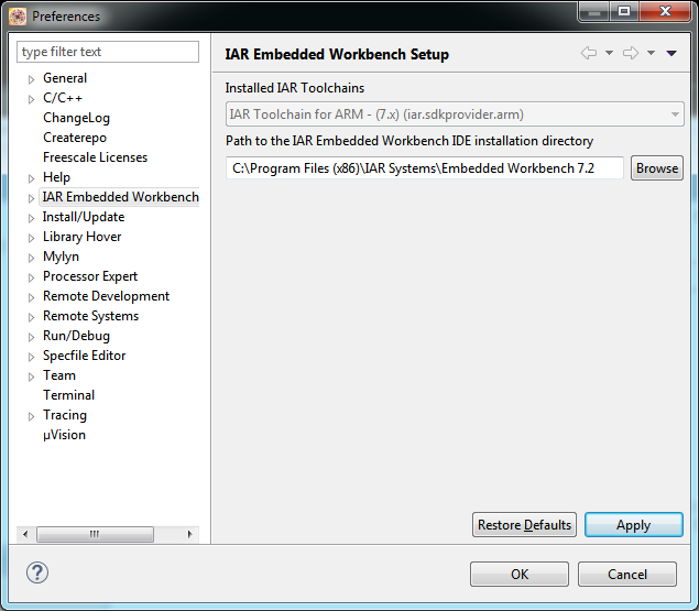
You may need to specify before this where to look for the IAR compiler, or else the previous item may hang.
The Add-On IAR for Eclipse, which is KDS, can be found here . I used the eclipse-iar-arm-7.20-201510121518.zip version. Add-On should be put before we start creating a project in KDS
(Click to enlarge)
As a result, we get the following project window:

(Click to enlarge)
Select the correct chip package ( Select Package in the Processor tab), since SKEAZN64 has several package options:
(Click to enlarge)
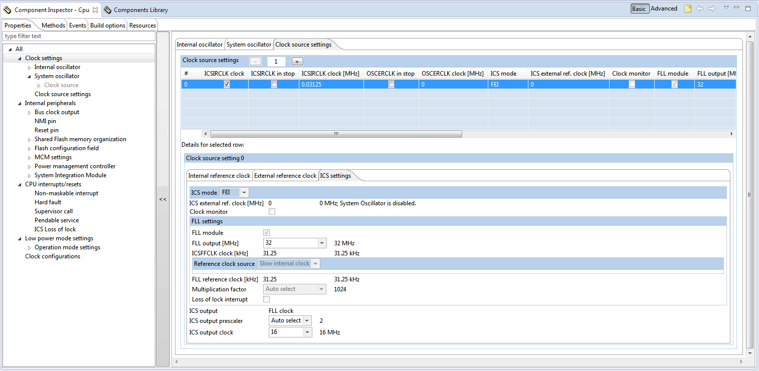
Clock system
To our convenience, the default clock initialization completely suits us and does not need to change anything. But the default frequency will be 32 MHz. This is more than enough. It is necessary to carefully study the tab Clock source settings shown in the screenshot below. Everything should be so.
(Click to enlarge)
Port initialization
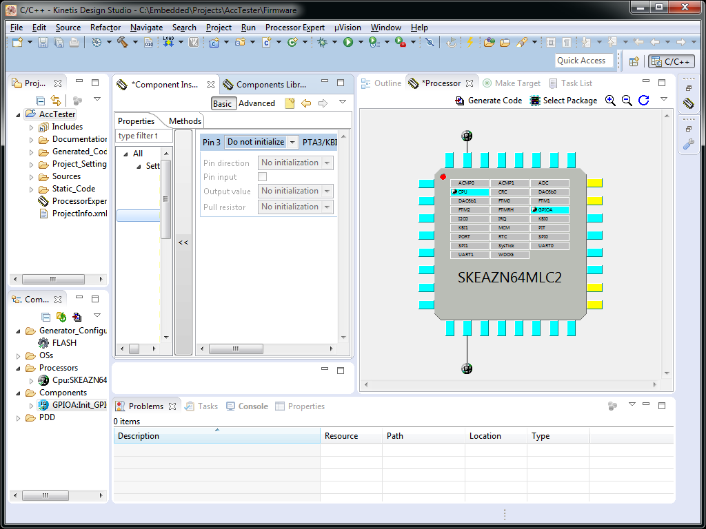
In the Components Library tab, select and paste into the Init_GPIO and Init_PORT project
Kinetis microcontrollers, as always, have a separation of pin functions into two peripheral modules: PORT and GPIO . PORT is responsible for the general properties of the port such as driver strength, the inclusion of port lines and the filters on the port lines. The GPIO is responsible for the operational management of the states of the pins individually and all together.
Therefore, it is necessary to configure the correct initialization in both modules.
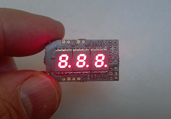
C Processor Expert can not rush and try to configure everything at once. You can easily get lost in obscure parameters and settings. First you need to understand the settings of the generator clock frequency of the core and bus of the microcontroller. Then try to bring the simplest external signal. This signal will be a illuminated segment on the 7th segment indicator.
In the PORT module, we initialize the pins PTD1 and PTC6 . In the GPIOA module I install 1 on these pins.
Click Project-> Generate Processor Expert Code ,
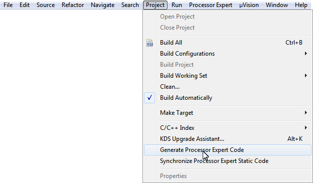
(Click to enlarge)
then Buil All .

(Click to enlarge)
If the process runs without errors, select Run-> Flash from file .. and F11 (Debug)

(Click to enlarge)
Segment lit
Initialization of the rest of the periphery
For further program development, we will need more ADC, SPI interface, and timers.
We drag the necessary periphery from the panel with the tab Components library into the panel with the tab Components
Should make this composition:

(Click to enlarge)
Here GPIOA and PORT have already been condemned. Added components PIT , SysTickInit , ADC , SPI0
Adding these components will cause the source code to be generated to initialize the corresponding peripherals.
And the purpose of the components in the context of this project is:
PIT is a periodic interrupt generator . Designed to generate signals to start the conversion of the ADC.
SysTickInit - ARM core system timer . Used by us for the periodic formation of interruptions in which the display is scanned.
ADC - ADC . In the first project, we will digitize not the external signal, but the signal of the internal temperature sensor.
SPI0 - SPI interface number 0. Needed to control the SPI key.
Here I no longer provide screenshots of the initialization of each of the components. In the source code laid out on github it will be possible to open the KDS project and consider everything.
It is not worth much to get involved in the configuration of different peripherals in Processor Expert . The fact is that this tool does not initialize all dependencies of the periphery. For example, we will need to run the ADC via a hardware trigger, but it will not be possible to configure it correctly in Processor Expert , since there is no installation of a hardware trigger channel in the SIM_SOPT register.
This somewhat complicates the task. A look into the KEA family programming manual will come soon. But not before I finish this article.
Migration to IAR
We click once again on the source generation command and turn on the IAR Embedded Workbench development environment.
Here, many people familiar with IAR may have a feeling of discomfort. After all, in IAR again and from scratch, it will be necessary to form a tree for the entire project, and even a project with an unknown directory structure. It comes to the aid of my project tree forming utility for IAR .
We form automatically a project tree in IDE IAR .
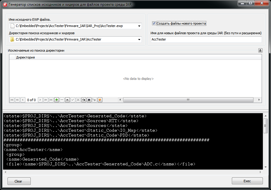
(Click to enlarge)
The IAR _Proj directory contains the IAR C.exe file along with the IAR workspace. This is an automatic project tree generation utility for IAR . It is used as follows:
1. If the IAR workspace has not yet been created, then it is created in the IAR IDE with the File-> New-> Workspace command. We give it the name AccTester for definiteness.
2. In the workspace, create an empty Project-> Create New Project ...
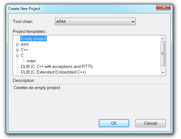
(Click to enlarge)
call it the same name as the workspace.
3. In the project, create an empty group and call it arbitrarily. Save the project. We get files with the .eww and .ewp extension and the same name.
(Click to enlarge)
4. Run the utility IARC.exe . The utility stores its settings in Ini.JSON and EscDirs.JSON . In the screenshot, it is configured to convert the project named AccTester.ewp and scan the directory tree with the root C: \ Embedded \ Projects \ AccTester \ Firmware_IAR \ AccTester
5. Press the Exec button.
6. The program passes recursively all directories starting from the root and skipping excluded directories. All C and and. H files found will be included in the IAR project file accordingly .
7. Open the .eww workspace file in IAR . In it we will see a project tree with groups following the directory structure. Then we can continue to customize the project options: select the type of microcontroller, configure the type of libraries, debugger, etc.
In the IAR_Proj directory there is already a prepared IAR workspace which can be studied.
The important thing is that by setting up an IAR in this way, we do not lose the opportunity to continue using Processor Expert . Only every time after the new generation of sources, and if this causes the appearance of new files, IARC.exe must be launched again and click the Exec button. The project in IAR then needs to be fully recompiled, but it takes a split second.
IAR project setup
IAR project set up for a long time is not necessary. The most important thing is to set the type of the microcontroller in the options window:

(Click to enlarge)
The default optimization will be minimal.
The file of the memory card with the extension .icf IAR uses from its own directory and it suits us.
In the debugger tab, select J-Link .

(Click to enlarge)
IAR has its own loader module for the microcontroller, just point out that they need to use. Check Use Flash Loader :

(Click to enlarge)
The structure of the source files of the project thermometer.
Processor Expert is able to generate initialization procedures and in it you can specify the flags for generating interrupt handlers from the periphery. But the generated handlers appear in the source texts for the corresponding periphery commented out. Therefore, the interrupt handlers from the ADC.c and SysTick.c files were manually transferred to the Events.c file and uncommented.
Important. If you plan to continue to use Processor Expert with IAR , then you need to be well aware of what files will be
overwritten, and in what files the information entered by us will be saved.
All files in the Generated Code directory will be overwritten .
The main.c file is also overwritten, but the line remains intact after the corresponding comment.
Here's what it looks like:
/*lint -save -e970 Disable MISRA rule (6.3) checking. */ int main(void) /*lint -restore Enable MISRA rule (6.3) checking. */ { /* Write your local variable definition here */ /*** Processor Expert internal initialization. DON'T REMOVE THIS CODE!!! ***/ PE_low_level_init(); /*** End of Processor Expert internal initialization. ***/ /* Write your code here */ Application(); /*** Don't write any code pass this line, or it will be deleted during code generation. ***/ /*** RTOS startup code. Macro PEX_RTOS_START is defined by the RTOS component. DON'T MODIFY THIS CODE!!! ***/ #ifdef PEX_RTOS_START PEX_RTOS_START(); /* Startup of the selected RTOS. Macro is defined by the RTOS component. */ #endif /*** End of RTOS startup code. ***/ /*** Processor Expert end of main routine. DON'T MODIFY THIS CODE!!! ***/ for(;;){} /*** Processor Expert end of main routine. DON'T WRITE CODE BELOW!!! ***/ } /*** End of main routine. DO NOT MODIFY THIS TEXT!!! ***/ /* END main */ Here I just added the string Application (); to transfer control to your procedure in the Indicator.c fileMore in the main.c file, I do not change anything.
Processor Expert also creates multiple files in the Static_code \ PDD directory. Practical benefit from them is small, I do not use them. They are essentially wrappers access to the registers of the periphery which can be accessed directly. The meaning of such files is the portability of projects from one type of microcontroller to another within the same family. They are needed more for developers of Processor Expert itself than for end users who do not have such an urgent need for on-line switching between microcontrollers within a single project.
All the application logic is concentrated in the Indicator.c file. It contains both the main loop and all interrupt handlers. The program is too small to break it into separate files.
And this is how the main application loop itself looks like:
void Application(void) { unsigned int uuid[2]; ADC_prepere(); Clear_display(); // RTT Get_unique_identificator(uuid); RTT_printf("\r\n\r\nS9KEAZN64AMLC (64 KB FLASH, 4 KB RAM) UUID=%08X-%08X\r\n", uuid[0], uuid[1]); // for (;;) { if (meas_done != 0) // { // float if (INTTEMPER_adcr > T25SMPL) { // 25 int_temperature = 25 - (INTTEMPER_adcr - T25SMPL) / (1000.0 * TSLOPE_LOW); } else { // 25 int_temperature = (T25SMPL - INTTEMPER_adcr) / (1000.0 * TSLOPE_HIGH) + 25; } Show_float("%0.1f", int_temperature); // RTT_printf("%0.3f\r\n", int_temperature); // RTT meas_done = 0; // , } } } The internal temperature sensor of the chip is used as a temperature sensor. Logging of measurement results is made to the RTT interface.
On the computer, the RTT interface is visible as a telnet port of the form: telnet: // localhost: 19021
You can connect to this port, for example, using the TeraTerm terminal emulator program with the following line:
"C:/Program Files (x86)/teraterm/ttermpro.exe" /T=1 telnet://localhost:19021 /X=0 /Y=0 /W="Jlink RTT" But we must remember that this port is open only when the IAR debugger is running via the J-Link adapter.When the adapter is disconnected, the port immediately closes.
Here is the output to the terminal.

(Click to enlarge)
The first three lines are displayed by the J-Link adapter itself.
That's all for now. Successful experiments with ARM Cortex-M0 +!
(Click to enlarge)
All sources are still available at https://github.com/Indemsys/Light-Control-Module-PCB
Source: https://habr.com/ru/post/367561/
All Articles