We design the board in KiCad with QEDA: from idea to prototype
Some time ago I published a presentation article about a tool called QEDA. In short, this is a utility to facilitate the process of creating a library of electronic elements.
Useful conclusions were made, further work was carried out, the project was developed. The command line interface (CLI) has appeared. Today we can talk about some milestone: the project has reached version 0.1 .
In this article I will look at a typical workflow for creating a board in KiCad environment and using the QEDA utility.
Warning : there will be pictures and, as a result, traffic.
Instead of preamble
Let me briefly remind you that you need to install Node.js to work, and then start it in the console (in * nix you may need sudo ):
npm install -g qeda And of course, we will need KiCad EDA , which also needs to be installed.
The development described below is carried out in Ubuntu Linux, but in the general case (probably with some amendments) it is possible in any OS.
At the moment, the project is sorely lacking documentation, but it is planned to be fixed in the future.
About the device
The device is an adapter for connecting the ESP-07 Wi-Fi module to the Pixhawk autopilot.
Formation of the library of elements
Actually this is the central part of our narrative.
If everything was established without errors, then a new command line utility should have appeared in the system. Check that this is the case - run in the console:
qeda --version If you see something like ...
QEDA v0.1.4 ... so we can continue.
To begin, choose a folder for the future project. In my case, this will be the wifi-adapter directory.
mkdir wifi-adapter cd wifi-adapter Step 1. Choosing a PCB manufacturer
In my case, I will create a library of elements with the requirements of a particular manufacturer. Of course, some parameters can be tweaked in the process of tracing in EDA, but here I will show how to take into account the production capabilities at the very first stage.
So, for example, take OSH Park . Of the most significant for us are the requirements for:
- minimum distance between conductors: 6 mil (0.2 mm) minimum spacing
- minimum hole diameter: 13 mil (0.4 mm) minimum drill size
- minimum width of the rim of the metallized hole: 7 mil (0.2 mm) minimum annular ring
In parentheses, I indicated the values converted to the metric system and rounded up to the tenths.
Create a folder for the future library of elements:
mkdir lib cd lib Now, using the qeda console command, qeda write the above restrictions. I repeat that while the teams are not documented, so far I will explain them in place.
qeda config pattern.clearance.padToPad 0.2 # qeda config pattern.minimum.drillDiameter 0.4 # qeda config pattern.minimum.ringWidth 0.2 # After executing these commands, a .qeda.yaml file will appear in the current directory, which stores all specified settings.
Step 2. Other settings
We can choose the preferred method for generating the chip pattern (pattern): recommended by the manufacturer or according to the IPC-7351 standard. The default is recommended by the manufacturer (default values are not required in the settings, but we will duplicate them to demonstrate the capabilities):
qeda config pattern.preferManufacturer true Those items whose descriptions do not contain manufacturer's recommendations are calculated according to the IPC-7351 standard. The standard provides for three levels of density (layout level):
- Least (
L) - the densest (recommended with limited dimensions of the printed circuit board) - Nominal (
N) - normal (recommended in most cases) - Most (
M) - the least dense layout (recommended for boards designed for harsh environments)
Since we are not limited in size, choose the least dense option:
qeda config pattern.densityLevel M Since it is supposed to solder the board manually, let's set one more parameter: the minimum distance from the output edge of the element to the opposite edge of its contact pad.
qeda config pattern.minimum.spaceForIron 0.5 It is also possible to configure the following parameters (in brackets are the default values):
pattern.clearance.padToMask(0.05): the distance from the edge of the contact pad to the edge of the mask (mask opening)pattern.minimum.maskWidth(0.2): minimum width of the mask belt (takes precedence over the previous parameter)pattern.lineWidth.silkscreen(0.12): thickness of the line in the screen printing layerpattern.fontSize.refDes(1.2): reference designator height
We will leave these parameters by default.
In addition, it is possible to set some settings for future conditional graphic symbols (HLO) of elements (schematic symbol):
symbol.style('default'): UGO tracing style, alternative: 'GOST'symbol.gridSize(2.5): anchor grid cell sizesymbol.fontSize.refDes(2.5): font height for reference designatorssymbol.fontSize.name(2.5): font height for the element namesymbol.fontSize.pin(2.5): font height to indicate conclusions
They also will not touch.
Step 3. Adding items
Since descriptions of the elements used are already contained in the element repository , we only need to list them. However, for interested persons, links to descriptions of the elements used are given in the spoiler below.
qeda add espressif/esp-07 # Wi-Fi qeda add capacitor/c0603 # 0603 qeda add capacitor/c1210 # 1210 qeda add resistor/r0603 # 0603 qeda add misc/tp-th-1 # (testpoint) qeda add ti/lm1117mpx # LDO qeda add hirose/df13a-6p-1.25h # If the required item is not in the repository, you need to create a library subdirectory and add the item description in YAML format.
Add more symbols of power and land:
qeda power +5V # +5 qeda power +3V3 # +3.3 qeda ground signal/GND # ( : 'chassis/', 'earth/' ) Step 4. Library generation
Well, here we come to the main and simplest step. Let's call our library wa .
qeda generate wa If the process has completed without errors, then two subdirectories should appear in the current lib directory:
librarycontaining cached YAML descriptions of the elements usedkicadwith KiCad library files
Everything: it's time to start drawing a scheme. Instructions for designing a circuit and a PCB are more like a well-known joke about how to draw an owl. However, this is due to the fact that the article is devoted mainly to the process of generating a library of elements, and the details of the design in KiCad would make the article even more bloated.
Circuit design
Create a KiCad project in the wifi-adapter/board directory.
Since our library of elements is self-sufficient, you can delete all the default KiCad libraries, and add only our wa :

We draw the scheme:

And in the style of GOST, the scheme would look like this:
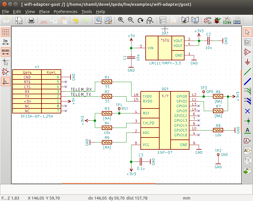
QEDA eliminates the need for such a stage as associating footprints to assignment footprints, as each element is already associated with a unique footprint. In other words, Cvpcb will not have to run.
We generate netlist.
PCB Design
To begin with, we also inform the editor that we need to draw seats from our newly baked wa library. To do this, create a file fp-lib-table with the following contents in the project directory:
(fp_lib_table (lib (name wa)(type KiCad)(uri ${KIPRJMOD}/../lib/kicad/wa.pretty)(options "")(descr "")) ) We import netlist, we do auto-spread.

Well, then "draw the rest of the owl." The tracer from me is not very good, so please do not judge strictly.

Realistic 3D:

We generate gerber'y and can be given to production.
Conclusion
On the simplest example, we reviewed the process of developing a printed circuit board, as they say, from scratch. I admit, the board did not reach production, but the pre-production control was successful.
Future plans:
- Test the utility on a more complex multi-layer board project and bring it to production.
- Document all settings and features.
- Start a web service that facilitates the work with the utility.
- To develop the service towards the support of new functions and different EDA.
Sources:
- Utility: https://github.com/qeda/qeda
- Item Descriptions: https://github.com/qeda/library
- Project
wifi-adapter: https://github.com/qeda/examples/tree/master/wifi-adapter
')
Source: https://habr.com/ru/post/367427/
All Articles