How to create semiconductor lasers. Part II

(Start here .)
By 1962, it became clear that the pn junction could be used as a laser. But at the same time he consumed a huge current, and therefore could only work in liquid nitrogen - otherwise overheating would quickly occur. Today we will learn how lasers have learned to work at room temperature and how far they have gone from their ancestors.
From pn transition to heterostructures
Lemma Kremera of misunderstanding
If, in discussing the problems of semiconductor physics, you cannot draw an energy band structure, then you do not understand what you are talking about.
It follows that if you can draw it, but do not do it, then your listeners do not understand what you are talking about.
One of the problems of the first lasers (as well as the entire semiconductor technology of the 50s – early 60s) was that the electric charges could not be localized in one area. Because of this, they "blurred" throughout the structure.
')

The band structure of the first laser in the middle of the pn junction. Electrons jump over the workspace and flow to the right. Holes, respectively, to the left.
The "diffused" electrons and holes were not just lost in vain, but in addition they still heated the structure. Of course, this led to an increase in the operating current and overheating of the device, and also reduced its speed. Herbert Krömer draws attention to this, suggesting in some way “bending” the band structure so that the distribution of carriers is limited by some kind of barrier:

After several unsuccessful attempts, a simple solution appeared: to use the boundary of two semiconductors with different width of the forbidden zone. In this case, the wider-gap semiconductor will act as a barrier for both electrons and holes:

Blue arrows - wide-gap semiconductor; red arrow - narrow-gap.
Later it turned out that this idea had already been proposed by William Shockley in 1948. He called it a “wide-gap emitter,” but Krömer proposed the name “ heterojunction ” or “ heterostructure, ” since the barrier was formed by nothing more than the boundary between two different materials.
So, with the advent of the heterojunction, carriers no longer flow away into the distance. But they can still come back, which is also not good. But what if we restrict the movement back by adding a second heterojunction from the other side? This idea almost simultaneously comes to mind both Krömer and Jores Alferov with Rudolf Kazarinov from the Ioffe Physicotechnical Institute. The use of a double heterostructure ( DGS ) promised a decrease in the operating current by a couple of orders of magnitude compared with the usual pn junction.

Laser diode on a double heterostructure. Electrons and holes are limited in space and do not spread anywhere.
Lyrical digression: how to understand zone structures
Zone structures are fine, but I want to understand what they correspond to in a real laser. In principle, to understand you need to remember only one thing: any laser consists of several layers, and on the band structure these layers are drawn from right to left. Say, the aforementioned double heterostructure:

consists of three layers: first (on the left) comes the n-semiconductor layer (electrons come from it), then the active region of material with a smaller band gap (electrons and holes are localized in it), and then the p-semiconductor layer. That is, it is like a pn junction, in the middle of which a narrow active layer is embedded. In reality, it looks like this:

From bottom to top: n-layer (red), active layer (yellow), p-layer (blue). Electrodes are attached to the top and bottom; the lower one also usually serves as a heat sink. Electrons and holes fall into the active layer and recombine there; laser radiation comes precisely from this layer.
consists of three layers: first (on the left) comes the n-semiconductor layer (electrons come from it), then the active region of material with a smaller band gap (electrons and holes are localized in it), and then the p-semiconductor layer. That is, it is like a pn junction, in the middle of which a narrow active layer is embedded. In reality, it looks like this:
From bottom to top: n-layer (red), active layer (yellow), p-layer (blue). Electrodes are attached to the top and bottom; the lower one also usually serves as a heat sink. Electrons and holes fall into the active layer and recombine there; laser radiation comes precisely from this layer.
The concept of a DGS laser was very simple, but to realize such a transition in practice turned out to be a very nontrivial matter. I wrote about the main reason in the story about blue LEDs : the transition from one semiconductor to another should occur without disrupting the crystal lattice. This means that the lattice constants (i.e. the distance between the atoms) of the two semiconductors should be almost the same. In the 1960s, various semiconductors were just beginning to be studied, and even the lattice constants of many of them were unknown. Therefore, on both sides of the ocean, scientists were busy searching for the "optimal pair" of semiconductors with identical lattice constants to easily grow a layer of one of them on the other. It took as long as five years for rather funny reasons, which are worth mentioning.
The Institute Ioffe quickly realized that the optimal pair is gallium arsenide with aluminum arsenide (GaAs-AlAs). But it turned out that AlAs is chemically unstable in the air due to water vapor. Unstable to such an extent that it had to explore in kerosene! Since the laser operation under normal conditions at room temperature was at stake, AlAs was immediately abandoned and switched to a slightly less promising pair of GaAs-GaAsP. GaAsP is a ternary compound, in fact, GaAs, in which part of the arsenic atoms (As) is replaced by phosphorus (P).
Two years later, it became clear that the GaAs-GaAsP laser basically works, but only at cryogenic temperatures. Due to the non-ideal matching of the permanent lattices, all attempts to work at room temperature turned into non-uniform thermal expansion and the propagation of defects at the heterojunction. In fact, when the current was turned on, the laser simply cracked along the boundary of the two materials.
At that moment, it turned out that a couple of years before that, someone at the institute had been growing AlGaAs crystals, which had become unnecessary in the writing desk. Due to the high aluminum content, it was believed that during this time they should decompose in humid air. Therefore, the news that nothing happened to crystals in a couple of years was very unexpected: it means that AlAs becomes stable when adding a small amount of gallium! (It should be added that today it is possible to work with pure AlAs: its thin layer, sandwiched between two other materials, contacts with air only along a very thin edge and therefore practically does not collapse.) The Alferov group switches to work with a pair of GaAs-AlGaAs, and By 1968, created the world's first laser operating at room temperature.
The problem of groups working in the USA (RCA, IBM, Bell Labs) turned out to be much more prosaic: they used the same tabular data for permanent grids in which the value for AlAs was incorrect. Because of this, a pair of GaAs-AlAs was not considered by them in principle, which delayed research for several years! The first of the American groups, the suitability of the GaAs-AlGaAs system was shown by Rupprecht and Woodall from IBM.
A little later, it turned out that DGS has another interesting advantage. A narrow-gap semiconductor (which is in the middle) usually has a higher refractive index than a wide-gap one. This means that it plays the role of an optical fiber: the light emitted in a narrow-gap layer does not go in all directions, but remains in it until it leaves the structure. This significantly increases the efficiency of the laser. Thus, DGS localizes not only electrons with holes, but also emitted light!
The creation of heterostructures turned out to be a giant breakthrough in microelectronics. He did not go unnoticed: Alferov and Creamer were awarded the Nobel Prize in 2000 for creating the DGS. Shockley received his Nobel Prize much earlier - in 1956, for opening the transistor.
Strip geometry
The laser, made by Alferov and his colleagues, worked at room temperature, but was pulsed. The next task was to make the laser working continuously. The main problem was still in the heat sink: during continuous operation, the central part of the laser simply overheated. They approached the solution from various sides: the American groups tried to attach an effective diamond heat sink to the laser, while the Soviet groups tried to use a narrow, elongated laser, not square. Both approaches proved to be successful, but the second - the creation of strip-geometry lasers - turned out to be much more practical. He did not need a diamond, and the processing of the crystal was much easier.

Laser with strip geometry. The active area is a narrow long strip from which heat is well rejected.
Lyrical digression: increasing power
It is possible to arrange several stripes side by side, thus increasing the laser power. This solution is somewhat reminiscent of multi-core processors: so that the chip that is too large and “stuffed up” does not overheat, it can be divided into several smaller chips. By and large, such lasers are manufactured using the same technology as integrated circuits. Curiously, the second half of the 2000 Nobel Prize was awarded for the creation of integrated circuits; got her jack kilby from texas instruments.
Resonator
In the first part, we learned that to create a mirror, you can polish the edges of the crystal or just gently chop them. You can also put or glue the mirrors outside - and it would seem that the ideas have been exhausted on this. By no means! In 1971, the Alferov group proposed using a periodic lattice deposited on the upper plane of the active layer.
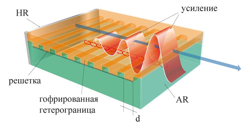
What is surprising is that this grating is not perpendicular to the laser beam (like our usual mirrors), but parallel to it! Despite this, such a grating not only works as an effective resonator, but also produces a well-collimated laser beam. This is called a distributed feedback laser.
Quantum wells
Let's close the two boundaries of DGS, reducing the thickness of the active layer. From a certain moment, the proximity of the barriers on both sides will begin to significantly affect the behavior of the electron. This is due to the quantization of the motion of an electron; therefore, such an object is called a quantum well .

The main feature of the quantum well is that electrons cannot be at the very bottom. The lowest level at which they can be located (in Figure E 1 ) is called the main (or first ) energy level of the quantum well and lies noticeably above its bottom. And still the electron can sit at higher energy levels - the second, the third and so on. Something like different electronic orbitals in atoms.
And now the most interesting: the depth of the ground level may vary depending on the width of the quantum well. That is, they made the quantum well layer wider — the level went deeper; narrower - level went up:

Quantum pits of different widths. Wider pit - lower level, and vice versa.
It turns out that by slightly changing the width of the quantum well, you can carefully adjust the energy of the laser transition, and hence the radiation wavelength! This new degree of freedom has opened the way for the creation of lasers with a virtually arbitrary wavelength (of course, within reasonable limits).
Lyrical digression: crystal growth
Today, crystal growth technologies with arbitrary thicknesses of layers based on GaAs are well established. But in a sense, this case is unsafe: both gallium and arsenic are highly poisonous. Some technical processes use arsine (AsH 3 ), an even more toxic gas with a faint smell of garlic. Of course, there are leak detectors in production, but experienced technologists know that if you smell garlic, you need to be in trouble.
... Once, in one scientific research institute on the night of April 1, when all technologists had already gone home, one joker decided to spread garlic cans with arsins. In the morning, technologists entered the room, breathed ... They say that evacuation was indeed announced, and what the technologists did to the prankster, history is silent :).
... Once, in one scientific research institute on the night of April 1, when all technologists had already gone home, one joker decided to spread garlic cans with arsins. In the morning, technologists entered the room, breathed ... They say that evacuation was indeed announced, and what the technologists did to the prankster, history is silent :).
Quantum cascade laser
A laser emits light when an electron falls from a higher energy level to a lower one. For example, from the conduction band to the valence band (like all lasers discussed above). Or, say, from the third level in the quantum well to the first:

An interesting idea, isn't it? It remains to somehow drive the electron to the upper level. It turned out to be the most effective to use tunneling from a neighboring quantum well (a similar idea was proposed by Rudolf Kazarinov and Robert Suris from the Joffe Institute in 1971). It will be even better if you put a lot of quantum wells next to it, so that the electron moves from one to another, emitting light:

Blue arrows - tunneling from the next hole, red - emission of light. The band structure is strongly tilted due to the applied voltage.
As you can see, the electron alternately emits a photon and tunnels into the adjacent hole, passing through several such cascades. For this reason, the laser was called quantum cascade . From the diagram it is clear that for his work it is necessary to precisely coordinate the energy levels in all quantum wells, which is not so simple. For the first time, Federico Capasso and colleagues at AT & T did it in 1994.
Of the features of a quantum cascade laser, it is worth noting that one electron makes it possible to obtain several photons, one per cascade. This undoubtedly increases the efficiency of the laser. And also the distance between the levels of the quantum well is very small, so the emitted photons have a longer wavelength. This allows you to create effective lasers emitting in the near and middle infrared range.
VCSEL
For all the above lasers, the radiation propagates perpendicular to the pn junction. In principle, no one bothers to make the radiation and the pn junction parallel. For this you need to slightly change the shape of the contacts and the location of the mirrors. It turns out like this:

GaAs-AlAs based laser. Blue layered structures (DBR) - multi-layered mirrors, I once told about them. The red layer between the mirrors is a quantum well, i.e. active region. Electrodes are shown in yellow, they are in contact with mirrors that conduct current to the active area. The upper ring electrode to transmit light through the middle; lower roundabout, because otherwise it is not done.
Right-top - laser eyes electron microscope. Who would guess why half of the layers of the mirror turned black from one edge, that’s a plus :).
As can be seen from the figure, this laser emits light not up to the side, but upwards. Such a VCSEL structure is called the vertical cavity surface emitting laser , translating literally a surface-emitting laser with a vertical resonator. This idea was first implemented in 1977 by the Kenichi Iga group from Tokyo, and it took several more years to optimize the lasers. The benefits of what came out were impressive:
- very low operating current
- low junction capacity and, as a result, high speed
- the ability to produce mirrors and active area in one stage of the process
- the ability to create a matrix of emitting diodes on a single crystal (and, for the same one stage of the process!)

Matrix VCSEL.
All of these properties have predetermined the use of VCSEL in telecommunications. Now they are already used for data transmission at a speed of 10 Gb / s, the possibility of creating diodes at higher speeds - up to 40 Gb / s - is being investigated.
Lyrical digression: some linguistics
In Russian, there is no established analogue of the term VCSEL. I like the abbreviation VIL - a vertically emitting laser. But more often use the English version with the pronunciation of "thumbs" or "bill". Sometimes this leads to incidents. Once in the media, a note about a new production of lasers under the working title “VekselCom” skipped; Some commentators have suggested that it was not without the famous businessman Vekselberg :).
And there is also a kind of VCSEL, which do not have a top mirror - instead of him an external mirror stands at some distance from the laser. They are called VECSEL - vertical external cavity surface-emitting laser. On hearing, the names do not differ at all! I don’t know how English speakers are struggling with this, but in Russian VECSEL is usually called a disc laser - its design is really similar to ordinary disc lasers.
And there is also a kind of VCSEL, which do not have a top mirror - instead of him an external mirror stands at some distance from the laser. They are called VECSEL - vertical external cavity surface-emitting laser. On hearing, the names do not differ at all! I don’t know how English speakers are struggling with this, but in Russian VECSEL is usually called a disc laser - its design is really similar to ordinary disc lasers.
Quantum filaments and quantum dots
As we saw above, the quantum well is a very thin layer of semiconductor. The electrons trapped in it become essentially two-dimensional: they cannot break out up or down, but can move back and forth and left-right. At the beginning of the 80s, the question arose: is it possible to further reduce the dimension of the active region (that is, to make a one-dimensional or zero-dimensional object), and if so, will there be any benefit from this?

Two-dimensional, one-dimensional and zero-dimensional structures.
Pretty soon managed to make such structures. One-dimensional began to be called a quantum thread or a quantum wire (“quantum wire”), zero-dimensional - a quantum dot (“quantum dot”). Their physics was extremely interesting; as for lasers, it turned out that the use of quantum dots makes it possible to further reduce the operating current of lasers. Their effectiveness can be compared with previous generations of lasers on visual graphics:

The evolution of laser diodes. Vertical - threshold current (the smaller, the easier it is to get the laser to work). Three dotted lines correspond to three generations of technologies: double heterostructures, quantum wells, quantum dots. Each next generation reduced the threshold current by about an order of magnitude.
The main problem of quantum dots is still the complexity of their manufacture: all semiconductor technologies are too sharpened for the growth of crystals “layer by layer”. But incredible prospects open up before them, and energy-efficient lasers are only a small part of them. Points in VCSEL-type structures exhibit a variety of quantum-optical effects; freestanding points can be used as sources of single and entangled photons; their magnetic properties allow us to consider them as promising qubits, and much more. But that's another story.
Sources
[1] Lecture of Zh. I. Alferov in the television program “Academia”, parts one and two .
[2] Nobel lectures on physics in 2000 in the translation of the journal Uspekhi Fizicheskikh Nauk .
[3] Kenichi Iga “Vertical-Cavity Surface-Emitting Laser: Its Conception and Evolution”, Jap. J. of Appl. Phys. 47 (1), 1 (2008).
Pictures from here: 1 , 2 , 3 , 4 , 5 , 6 , 7 , 8 , 9 .
Source: https://habr.com/ru/post/366715/
All Articles