Unique Nanocomposite for contacts in electrical network switches
Today we will tell you about the Research Center "Structural Ceramic Nanomaterials" and how to get a unique nanocomposite for contacts in switches of electrical networks. A large photo report awaits you with a step-by-step description of how to obtain the final product using the method of high-energy processing of metal powders in a ball mill, followed by the consolidation of the resulting nano-structured composite particles by the method of spark plasma sintering. Especially for our corporate blog on GT, center engineer Kirill Kuskov did a whole experiment that will be of interest to the target audience: engineers and specialists from relevant areas. The resulting composite differs from its predecessors in high energy efficiency, efficiency and reliability.
The Research Center for Structural Ceramic Nanomaterials (SIC KKN) was founded in June 2011 at the National Research and Technical University "MISiS" under the guidance of the leading scientist Dr.Sc. A. S. Mukasyan , who is also a professor at the Faculty of Chemical and Biomolecular Engineering at the University of Notre Dame (USA).
Since the establishment of the center, the main fundamental area of research has been the use of the "solid flame" phenomenon for the synthesis of ceramic and metal nanopowders, as well as the study of the fundamental principles of their sintering in order to obtain new materials based on them. At the initial stage, three fundamentally new directions were singled out: ceramic nano materials, metal catalysts, and the combination of refractory and dissimilar materials.

The main focus was on the study of the mechanisms of heat and mass transfer in heterogeneous nanostructured media under conditions of high temperatures and fast chemical reactions in order to create technologies for the production of nanomaterials with improved physicomechanical properties.
')
All three areas of research proposed in this project are aimed at solving actual applied problems. The technologies created on the basis of these studies will find application in such fields of science and technology as cosmonautics and aviation technology, the chemical and defense industries, oil and gas production, and many others.
Recently, a new method of producing nanocomposite materials based on metal pseudo-alloys (Cr-Cu, W-Cu, etc.) was developed for their use as contacts in switches of high-power electrical networks operating under high current and high voltage conditions in order to increase their energy efficiency , profitability and reliability. The method consists in the combination of high-energy treatment of metal powders in a ball mill with subsequent consolidation, obtained nano-structured composite particles, using spark plasma sintering (IPA). IPA allows you to save nano-structure in sintered non-porous materials, which causes their unique electrophysical, thermal-physical and mechanical properties.

The first step in the synthesis of pseudo-alloy is the processing of the initial powders in a planetary ball mill. Since the processing takes place in the field of centrifugal forces under high loads, it is necessary to balance the drums with the grinding bodies (in our case with the balls).

Then prepared the sample source materials


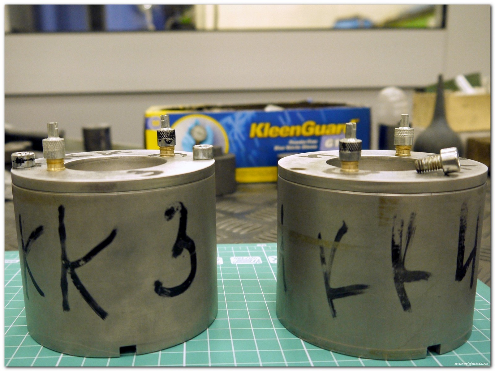
The prepared samples are loaded into the drum.


Loaded drums are closed with a lid. Air is pumped out through special valves in the lid, and then the drum is filled with inert gas (argon).

Since the heat from the balls is removed through the gas atmosphere, better cooling can be provided inside the drum by starting 2-3 atmospheres of argon.

Then the drums are placed in special holders and secure

In a ball planetary mill, the motion of the balls is controlled by two parameters: the ratio of the radii of rotation of the central axis and the radius of the drums and their ratio of speeds. The radii are determined by the design of the mill and are constant.
The design of the mill allows with high accuracy to withstand the ratio of speeds, i.e. ball motion mode. When grinding the same powders in different modes, you can get significantly different results. To control the temperature there is water cooling outside the drums.

The speed of the planetary rotation and rotation of the drums with the appropriate design can be changed. The laboratory planetary mill "Activator-2S" has a separate drive to the central axis and to the drums, which allows the drum mode, shear, vortex, or a combination of them to be realized in the drum.


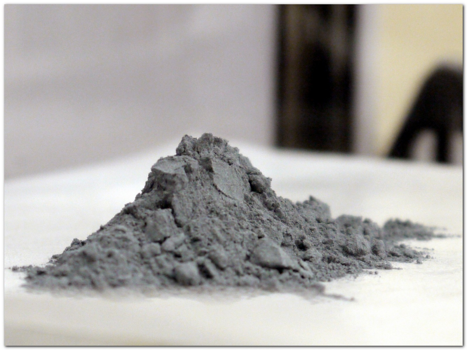
After processing in the mill, the drums are opened and the resulting powder, which is a composite particle, in which nanometer-sized copper and chromium particles are uniformly mixed, is extracted using a sieve.


The IPA method uses pulses of direct electric current passing through the graphite matrix in which the sample is located. The process consists essentially of the combined effects of temperature, axial pressure and electric current in the presence of an electromagnetic field.
The resulting mixture is loaded into the prepared graphite matrix.

Depending on the purpose of the sample and the process conditions, the inner diameter of the matrix is chosen, which predetermines the size of the future tablet and the possibility of using graphite paper as a layer to facilitate removal after sintering.

To evenly distribute the load, the distance from the edges of the punches to the die is aligned.

The loaded matrix is installed between the electrodes of the installation. The upper electrode is fixed and the lower one is mobile.

To fix the matrix, a small initial pressure is set on the control panel.

The control panel is a touch panel, levers of power control of the supplied charge and the load on the punches and the emergency stop button


The chamber is evacuated and water cooling starts.

The vacuum pump is connected to the working chamber through a filter and valve

A pyrometer is focused on a sample through a special window to record the temperature during the process.

Focusing is made on a special hole in the wall of the matrix

Each sintering is recorded in a laboratory journal, which indicates the sintering number, conditions, sintering material, as well as notes on the processes and phenomena that occur during the experiment.

The installation allows sintering both in fully automatic mode and in manual mode, with the programs for heating and load being independent and set separately

When using the automatic mode, the operator at any time of the process, if necessary, can switch to manual and adjust the process conditions

During sintering, the generators are cooled by four fans. Current is applied to the electrodes through special tires.


At the end of the process the sample cools. The cooling time depends on the sintering temperature and the size of the mold. After cooling into the chamber, air is let in and the matrix is removed.

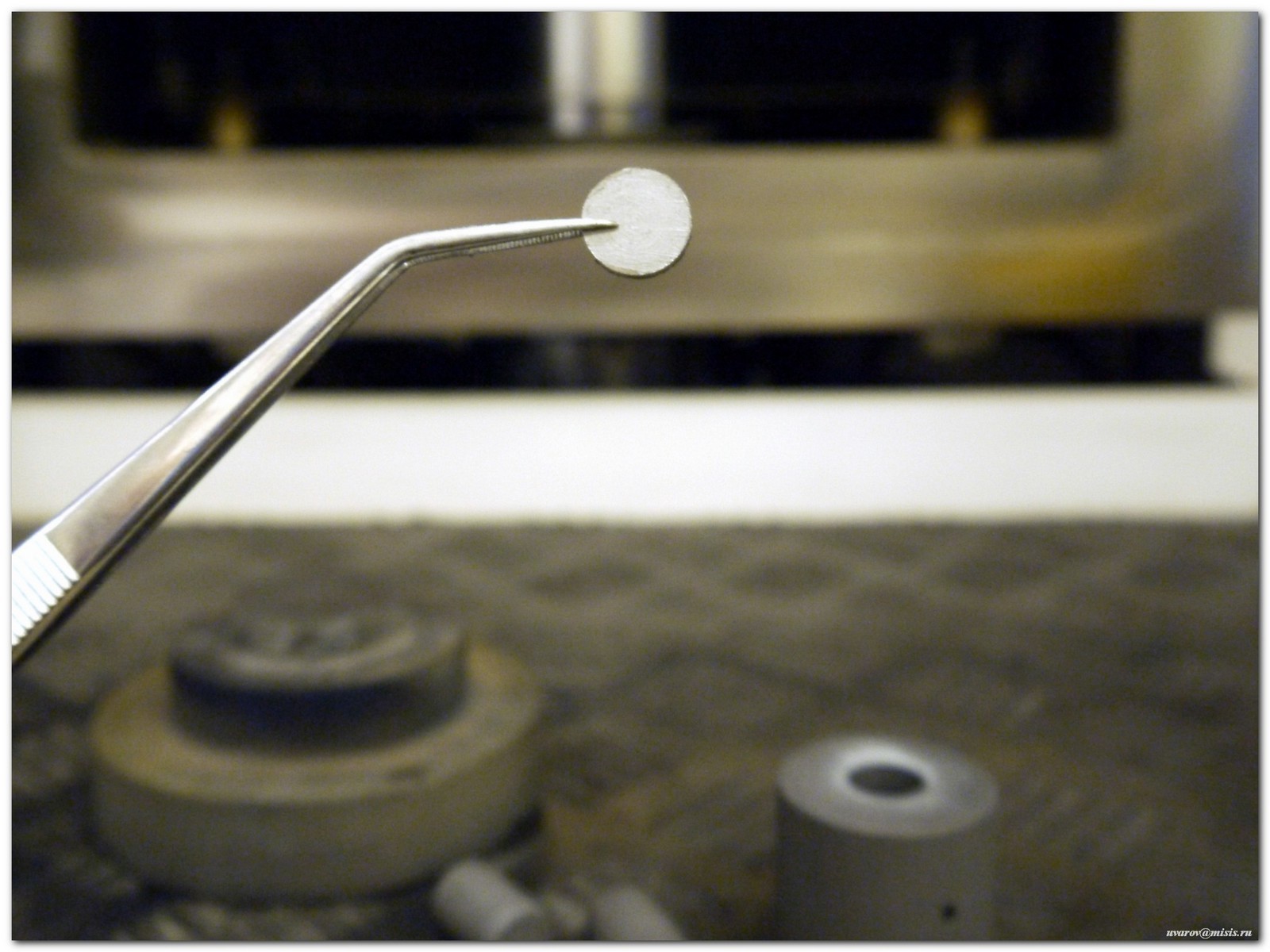
Then, punches and a sample are extruded from the die.

- Uniform heat distribution over the sample
- Preliminary processing by pressure is not required
- Uniform sintering of homogeneous and dissimilar materials
- Short cycle time
- Removal of existing impurities
- Production of the part immediately in final form and obtaining a profile close to the specified
- Minimum grain growth
- Minimal impact on the microstructure.


The final size depends on the shape of the matrix and the amount of powder.

Installation of spark plasma sintering (IPA) (Spark Plasma Sintering - Labox 650, Sinter Land, Japan)

The IPA method uses pulses of direct electric current passing through the graphite matrix in which the sample is located. The process consists essentially of the combined effects of temperature, axial pressure and electric current in the presence of an electromagnetic field (plasma). High local temperatures between the particles evaporate pollutants and oxides on the surface of the particles before the formation of a jumper. This effect with the simultaneous application of axial pressure can significantly reduce the sintering temperature and the duration of the process, which, in turn, contributes to a significant decrease in the rate of grain growth, in contrast to sintering without load or hot pressing.
At the IPS facility, powders of pseudo-alloys of immiscible metals Cu and Cr were consolidated with a characteristic size of heterogeneity of the structure of 2.5 nm. It was shown that the proposed combined HEMO + IPA method allows to reduce the grinding time to 60 minutes and the sintering time under a pressure of 50 MPa at a temperature of 700-900 º to 5 minutes. During consolidation, grain growth and ordering of the crystal structure occur, but in the final consolidated material the nanostructure is preserved with characteristic phase sizes of 5-60 nm (chromium phase) and 200-300 nm (copper matrix phase). The material has a Vickers hardness of 3.89 GPa and an electrical resistivity of 7.15 µOhm · cm. These properties make it promising for use in the contacts of high current vacuum switches.
I would also like to say that a scientific article “Bulk Cu – Cr nanocomposites sintering, Journal of Alloys and Compounds” (2014) was published on the topic of this experiment by a team of the “Construction Ceramic Nanomaterials” center.
Samples of alloys under the microscope: used in industry (left) and obtained by a new method (right)

The technologies that will be created on the basis of these studies will find applications in such areas as cosmonautics, aviation technology, chemical and defense industries, oil and gas production, and many others.
The Research Center for Structural Ceramic Nanomaterials (SIC KKN) was founded in June 2011 at the National Research and Technical University "MISiS" under the guidance of the leading scientist Dr.Sc. A. S. Mukasyan , who is also a professor at the Faculty of Chemical and Biomolecular Engineering at the University of Notre Dame (USA).
Since the establishment of the center, the main fundamental area of research has been the use of the "solid flame" phenomenon for the synthesis of ceramic and metal nanopowders, as well as the study of the fundamental principles of their sintering in order to obtain new materials based on them. At the initial stage, three fundamentally new directions were singled out: ceramic nano materials, metal catalysts, and the combination of refractory and dissimilar materials.
The main focus was on the study of the mechanisms of heat and mass transfer in heterogeneous nanostructured media under conditions of high temperatures and fast chemical reactions in order to create technologies for the production of nanomaterials with improved physicomechanical properties.
')
All three areas of research proposed in this project are aimed at solving actual applied problems. The technologies created on the basis of these studies will find application in such fields of science and technology as cosmonautics and aviation technology, the chemical and defense industries, oil and gas production, and many others.
Recently, a new method of producing nanocomposite materials based on metal pseudo-alloys (Cr-Cu, W-Cu, etc.) was developed for their use as contacts in switches of high-power electrical networks operating under high current and high voltage conditions in order to increase their energy efficiency , profitability and reliability. The method consists in the combination of high-energy treatment of metal powders in a ball mill with subsequent consolidation, obtained nano-structured composite particles, using spark plasma sintering (IPA). IPA allows you to save nano-structure in sintered non-porous materials, which causes their unique electrophysical, thermal-physical and mechanical properties.
 Especially for our corporate blog on GT, center engineer Kirill Kuskov did the whole experiment Graduate student SRC "Structural Ceramic Nanomaterials" Engineer |
Then prepared the sample source materials
The mass of the sample depends on the desired composition of the final pseudo-alloy, as well as on the specified ratio of the mass of the balls to the mass of the powder, which greatly affects the structure of the powder.
The prepared samples are loaded into the drum.
Loaded drums are closed with a lid. Air is pumped out through special valves in the lid, and then the drum is filled with inert gas (argon).
Since the heat from the balls is removed through the gas atmosphere, better cooling can be provided inside the drum by starting 2-3 atmospheres of argon.
Then the drums are placed in special holders and secure
In a ball planetary mill, the motion of the balls is controlled by two parameters: the ratio of the radii of rotation of the central axis and the radius of the drums and their ratio of speeds. The radii are determined by the design of the mill and are constant.
The design of the mill allows with high accuracy to withstand the ratio of speeds, i.e. ball motion mode. When grinding the same powders in different modes, you can get significantly different results. To control the temperature there is water cooling outside the drums.
The speed of the planetary rotation and rotation of the drums with the appropriate design can be changed. The laboratory planetary mill "Activator-2S" has a separate drive to the central axis and to the drums, which allows the drum mode, shear, vortex, or a combination of them to be realized in the drum.
Asynchronous motors are controlled by inverters, which are networked and connected to a computer. The control program sets the rotation speed for each drive, the acceleration and the rotation time.
After processing in the mill, the drums are opened and the resulting powder, which is a composite particle, in which nanometer-sized copper and chromium particles are uniformly mixed, is extracted using a sieve.
The next stage is the consolidation of the obtained composite material by the method of spark plasma sintering.
The IPA method uses pulses of direct electric current passing through the graphite matrix in which the sample is located. The process consists essentially of the combined effects of temperature, axial pressure and electric current in the presence of an electromagnetic field.
The resulting mixture is loaded into the prepared graphite matrix.
Depending on the purpose of the sample and the process conditions, the inner diameter of the matrix is chosen, which predetermines the size of the future tablet and the possibility of using graphite paper as a layer to facilitate removal after sintering.
To evenly distribute the load, the distance from the edges of the punches to the die is aligned.
The loaded matrix is installed between the electrodes of the installation. The upper electrode is fixed and the lower one is mobile.
To fix the matrix, a small initial pressure is set on the control panel.
The control panel is a touch panel, levers of power control of the supplied charge and the load on the punches and the emergency stop button
On the touch panel, you can set sintering programs and load applications, control the vacuum system and the gas supply system, set the parameters of current pulses; during sintering allows you to monitor the displacement of the punches, temperature, voltage, amperage. Above the touch panel is a pressure sensor in the chamber.
The chamber is evacuated and water cooling starts.
The vacuum pump is connected to the working chamber through a filter and valve
A pyrometer is focused on a sample through a special window to record the temperature during the process.
Focusing is made on a special hole in the wall of the matrix
Each sintering is recorded in a laboratory journal, which indicates the sintering number, conditions, sintering material, as well as notes on the processes and phenomena that occur during the experiment.
The installation allows sintering both in fully automatic mode and in manual mode, with the programs for heating and load being independent and set separately
When using the automatic mode, the operator at any time of the process, if necessary, can switch to manual and adjust the process conditions
During sintering, the generators are cooled by four fans. Current is applied to the electrodes through special tires.
During the process, all data is recorded in a special program and saved to a file. The frequency of fixing data from the devices is set by the operator. This data can then be used to calculate the sintering kinetics.
At the end of the process the sample cools. The cooling time depends on the sintering temperature and the size of the mold. After cooling into the chamber, air is let in and the matrix is removed.
Then, punches and a sample are extruded from the die.
Advantages of the spark plasma sintering method:
- Uniform heat distribution over the sample
- Preliminary processing by pressure is not required
- Uniform sintering of homogeneous and dissimilar materials
- Short cycle time
- Removal of existing impurities
- Production of the part immediately in final form and obtaining a profile close to the specified
- Minimum grain growth
- Minimal impact on the microstructure.
The final size depends on the shape of the matrix and the amount of powder.
Installation of spark plasma sintering (IPA) (Spark Plasma Sintering - Labox 650, Sinter Land, Japan)
The IPA method uses pulses of direct electric current passing through the graphite matrix in which the sample is located. The process consists essentially of the combined effects of temperature, axial pressure and electric current in the presence of an electromagnetic field (plasma). High local temperatures between the particles evaporate pollutants and oxides on the surface of the particles before the formation of a jumper. This effect with the simultaneous application of axial pressure can significantly reduce the sintering temperature and the duration of the process, which, in turn, contributes to a significant decrease in the rate of grain growth, in contrast to sintering without load or hot pressing.
 Dmitry Moskovskikh Candidate of Technical Sciences SRC "Structural Ceramic Nanomaterials" Researcher |
| I also want to note that our center is developing other truly unique ways of producing materials. From the name of the center it will be logical to touch on the topic of ceramics, namely silicon carbide (SiC). Materials based on SiC have unique properties, such as low theoretical density (lightness), high strength and hardness, heat resistance and oxidation resistance. These properties cause very wide areas of application, such as astronautics, aviation technology, defense industry, oil and gas production, microelectronics. At the same time, existing methods for producing such a material, such as, for example, Acheson's method, based on the reduction of silicon dioxide (SiO2) with carbon, are characterized by high temperatures (> 2000 K) and a long process time (30 - 150 hours), which does not meet current trends development of science and technology in the field of obtaining materials. The laboratory has developed a new method for direct production of nanostructured (SiC grain size <100 nm) of non-porous carbide silicon ceramics by combining solid-flame combustion (or self-propagating high-temperature synthesis) and spark plasma sintering. By passing a pulsed electric current through the matrix, the material is heated. After reaching a certain temperature in the matrix, the formation of silicon carbide occurs, which is subsequently sintered.  The process consists essentially of the combined effects of temperature, axial pressure and electric current in the presence of an electromagnetic field (plasma). High local temperatures between the particles evaporate pollutants and oxides on the surface of the particles before the formation of a jumper. Joule heat concentrates on the surface of already “clean” particles, causes their plastic deformation, which contributes to the achievement of a high density of the material being consolidated. Through the use of such a unique installation and method developed at NITU "MISiS", it is possible to significantly reduce the temperature and time of production of silicon carbide (compared to traditional methods). At the same time, the microstructure and properties of materials are completely identical to those for ceramics obtained by sintering SHS nanopowders, but it is possible to exclude the stage of synthesis of SiC powder and reduce the sintering time. |
Results:
At the IPS facility, powders of pseudo-alloys of immiscible metals Cu and Cr were consolidated with a characteristic size of heterogeneity of the structure of 2.5 nm. It was shown that the proposed combined HEMO + IPA method allows to reduce the grinding time to 60 minutes and the sintering time under a pressure of 50 MPa at a temperature of 700-900 º to 5 minutes. During consolidation, grain growth and ordering of the crystal structure occur, but in the final consolidated material the nanostructure is preserved with characteristic phase sizes of 5-60 nm (chromium phase) and 200-300 nm (copper matrix phase). The material has a Vickers hardness of 3.89 GPa and an electrical resistivity of 7.15 µOhm · cm. These properties make it promising for use in the contacts of high current vacuum switches.
I would also like to say that a scientific article “Bulk Cu – Cr nanocomposites sintering, Journal of Alloys and Compounds” (2014) was published on the topic of this experiment by a team of the “Construction Ceramic Nanomaterials” center.
Samples of alloys under the microscope: used in industry (left) and obtained by a new method (right)
The technologies that will be created on the basis of these studies will find applications in such areas as cosmonautics, aviation technology, chemical and defense industries, oil and gas production, and many others.
Source: https://habr.com/ru/post/366615/
All Articles