Homemade cartridges for Dendy / Famicom
After my article about dumper cartridges (which for some reason was left on Habré for some reason), I was asked many times to tell how to collect and write cartridges for Dandy / Famicom myself. Yes, this is a very hackneyed topic, even in the ancient issues of Radio magazine one could read about it, but progress does not stand still. Consider this topic in terms of modern components. Moreover, in my opinion, it is ideal for learning the basics of working with FPGAs, this is where I myself studied.
Like last time, this publication is in two formats: entertaining video is simpler (yes, already the third series) and a regular article with more detailed information. Who likes more, but look better and then, and more.
')
Video:
Article:
You probably need to start with the fact that the cartridges that were sold and continue to be sold in our stores, alas, cannot be overwritten (in fact, some are possible, but more on that another time). This is due to the fact that they installed the usual EPROM memory, which can be written only once. However, nothing prevents you from collecting your own cartridge from scratch.
Let me remind you that the cartridge is inserted directly into the CPU bus and into the PPU bus, and accordingly, first of all it contains two memory chips with parallel access: PRG - the processor accesses it, and it contains the game code itself, and CHR - the PPU works with it (graphical processor) and it contains images. Moreover, the latter can easily be not a ROM, but a random access memory, where data is already recorded during the game.
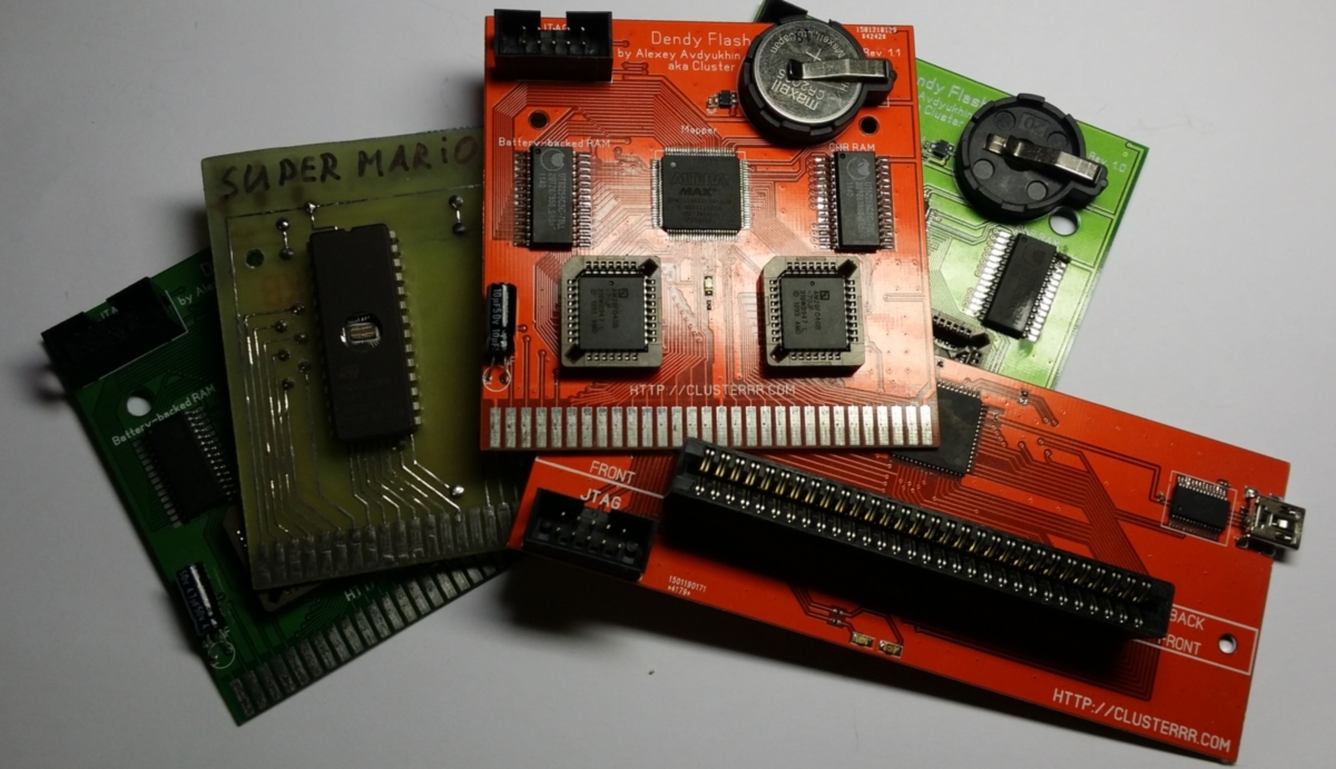
Thus, the simplest cartridge can be made from any two memory chips with parallel access, be it at least an EPROM, even a flash. In this case, nothing more of the strapping is needed. For example, this is how my first self-made cartridge looked like:

Chips are simply connected directly to the corresponding pins on the cartridge connector. Feet / RD can be soldered directly to the ground, because the console will always only read the data, but I recorded the data after the cartridge was assembled, using the same dumper , so I connected all the conclusions as expected. The bits of the address and data are mixed up in this way, but it absolutely does not matter. At the bottom you can see a jumper that defines “mirroring” - how the video memory will be mirrored horizontally or vertically. It depends on the game, and in the simplest games it was determined by the jumper on the cartridge.
And another very important point - you need to activate our memory only when the console accesses the cartridge, otherwise there will be a conflict on the bus. To do this, the chip has output / CE (chip enable), which includes memory. Here in the course goes a fairly simple math. Program ( PRG ) cartridge memory starts at $ 8,000 and ends at $ FFFF , two to the fifteenth power. Graphic ( CHR ) cartridge memory starts at $ 0000 and ends at $ 1FFF , having a volume of 8 kilobytes, which is two to the thirteenth power. Accordingly, our memory should be turned on with the fifteenth and thirteenth contacts on the address bus. On the cartridge connector there are already special leads that give us the signal we need. Moreover, in the case of PRG memory, the contact we need is called - / ROMSEL - abbreviated as ROM Select. There the console produces 0 volts when it accesses the cartridge's memory in the area between $ 8000 and $ FFFF . Everything is easier nowhere.
However, it will be possible to record only the simplest games on such a cartridge. More serious ones already use mapper cartridges to increase the maximum volume of the game. I'll try to explain how they worked.
In memory with parallel access, each bit of the address is set by a separate output from the chip. In the cartridge connector there are pins A0-A14 (15 pins) for PRG memory. These are respectively 15 bits of the address, which give 32768 combinations of ones and zeros, i.e. allow you to address 32 kilobytes. For the CHR memory there, respectively, the pins A0-A13 are 16384 combinations, i.e. 16 kilobytes, but half of them are allocated to the memory inside the console.
Already in the eighties such volumes began to be missed. Of course, nothing prevents you from putting a large amount of memory in the cartridge, but this memory has more address and pin outputs. It is not difficult to calculate that each additional output doubles the number of possible addresses exactly. But where to connect them if the number of contacts in the cartridge connector is limited? This is where the mappers come to the rescue, it is they who manage the additional conclusions depending on various conditions. Almost always, such conditions are attempts to write to the PRG-area of the cartridge memory. Yes, the one where you can not write anything.
Many games use simple logic chips for this purpose. For example, in a cartridge, Battletoads has a four-bit counter 74161 , which is used as a trigger. When writing to any address from $ 8000 to $ FFFF, he memorizes the recorded value and gives it to the very additional conclusions from the memory, he also switches the mirroring.
But most games use more complex chips for this purpose, which are designed specifically for this purpose.
They, as a rule, are already able to switch different banks for different memory areas, manage additional memory, generate interrupts, and sometimes even expand the computing power of the console.
As an example, take the most popular mapper - MMC3 . You can read about it in detail here: wiki.nesdev.com/w/index.php/MMC3
First of all, we read how it interacts with it. And it happens through writing to certain addresses, their 8 groups: $ 8000- $ 9FFE (even), $ 8001- $ 9FFF (odd), $ A000- $ BFFE (even), $ A001- $ BFFF (odd), $ C000- $ DFFE (even), $ C001- $ DFFF (odd), $ E000- $ FFFE (even) and $ E001- $ FFFF (odd). Writing to any address within the group is equivalent. See the pattern? The register is selected using the three address bits: A0 , A13 and A14 , while the others have no values.
Let's try to imitate the work of the mapper using FPGA. I write the code in the Verilog language. It is not highlighted here, I apologize for this.
First, we describe our registers that store the current state:
reg [2:0] bank_select; reg prg_mode; reg chr_mode; reg [7:0] r [0:7]; reg mirroring; reg [7:6] ram_protect; reg [7:0] irq_latch; reg [7:0] irq_counter; reg [2:0] a12_low_time; reg irq_reload; reg irq_reload_clear; reg irq_enabled; We describe the reaction to the entry at the appropriate addresses. The rising signal / ROMSEL is talking about the fact that there was a memory access to the cartridge, at addresses $ 8000- $ FFFF , we need to respond at this very moment.
always @ (posedge romsel) begin // if (cpu_rw_in == 0) begin // A14, A13 A0, case ({cpu_addr_in[14:13], cpu_addr_in[0]}) 3'b000: begin // $8000-$9FFE, even bank_select <= cpu_data_in[2:0]; prg_mode <= cpu_data_in[6]; chr_mode <= cpu_data_in[7]; end 3'b001: r[bank_select] <= cpu_data_in; // $8001-$9FFF, odd 3'b010: mirroring <= cpu_data_in[0]; // $A000-$BFFE, even 3'b011: ram_protect <= cpu_data_in[7:6]; // $A001-$BFFF, odd 3'b100: irq_latch <= cpu_data_in; // $C000-$DFFE, even 3'b101: irq_reload <= 1; // $C001-$DFFF, odd 3'b110: irq_enabled <= 0; // $E000-$FFFE, even 3'b111: irq_enabled <= 1; // $E001-$FFFF, odd endcase end if (irq_reload_clear) irq_reload <= 0; end Now we will describe which bank should be selected when accessing the corresponding part of the memory, depending on our registers.
They are switched according to this table:
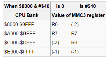
Where $ 8000 & # $ 40 is our prg_mode, and -2 and -1 are the last and last bank respectively. Such code turns out:
// PRG banking always @ (*) begin case ({cpu_addr_in[14:13], prg_mode}) // $8000-$9FFF 3'b000: cpu_addr_out[18:13] <= r[6][5:0]; 3'b001: cpu_addr_out[18:13] <= 6'b111110; // // $A000-$BFFF 3'b010, 3'b011: cpu_addr_out[18:13] <= r[7][5:0]; // $C000-$DFFF 3'b100: cpu_addr_out[18:13] <= 6'b111110; // 3'b101: cpu_addr_out[18:13] <= r[6][5:0]; // $E000-$FFFF - default: cpu_addr_out[18:13] <= 6'b111111; endcase // A12 MMC3 , cpu_addr_out[12] <= cpu_addr_in[12]; end Now CHR. There is such a scheme:

Where $ 8000 & # $ 40 is chr_mode. It turns out like this:
// CHR banking always @ (*) begin if (ppu_addr_in[12] == chr_mode) ppu_addr_out[17:10] <= {r[ppu_addr_in[11]][7:1], ppu_addr_in[10]}; else ppu_addr_out[17:10] <= r[2+ppu_addr_in[11:10]]; // CHR MMC3 - 256 , A18 0. ppu_addr_out[18] <= 0; end The mirroring mode is described in just one line. Depending on it, we close the output of the CIRAM A10 cartridge to either the A10 or the A11 :
assign ppu_ciram_a10 = mirroring ? ppu_addr_in[11] : ppu_addr_in[10]; Further more difficult. MMC3 can generate interrupts when a certain string is drawn on the screen. This is very useful, and games often use it. Lines on the screen are counted by referring to A12 on the PPU. With typical settings, the signal on A12 goes from logical 0 to logical 1 exactly once per line, short of transitions to 0. And they should not be counted, this complicates things a bit:
// , A12 always @ (*) begin if (!irq_enabled) begin irq_ready = 0; irq <= 1'bZ; end else if (irq_enabled && !irq_value) irq_ready = 1; else if (irq_ready && irq_value) irq <= 1'b0; end // always @ (posedge ppu_addr_in[12]) begin if (a12_low_time == 3) // A12 3 CPU begin if ((irq_reload && !irq_reload_clear) || (irq_counter == 0)) begin irq_counter = irq_latch; if (irq_reload) irq_reload_clear <= 1; end else irq_counter = irq_counter-1; if (irq_counter == 0 && irq_enabled) irq_value = 1; else irq_value = 0; end if (!irq_reload) irq_reload_clear <= 0; end // A12 3 CPU always @ (posedge m2, posedge ppu_addr_in[12]) begin if (ppu_addr_in[12]) a12_low_time <= 0; else if (a12_low_time < 3) a12_low_time <= a12_low_time + 1; end Oh yeah, MMC3 also supports connecting additional RAM at $ 6000- $ 7FFF ! We must not forget and describe it:
assign cpu_wr_out = cpu_rw_in || ram_protect[6]; assign cpu_rd_out = ~cpu_rw_in; assign cpu_sram_ce = !(cpu_addr_in[14] && cpu_addr_in[13] && m2 && romsel && ram_protect[7]); That's it, our MMC3 is ready! The full code can be found here: https://github.com/ClusterM/nes_mappers/blob/master/4%20(MMC3)/MMC3.v
In the same repository there are codes of many other mappers.
In fact, it is very simple to assemble a cartridge for any one particular game, because you only need to install the necessary components. But to make a universal cartridge is much more difficult. If you install the FPGA on 128 macrocells, 512 kilobytes flash for PRG, 512 kilobytes flash for 32 kr for CHR, 32 kilobytes for CHR, 32 kilobytes for SRR as additional memory, which is powered by a battery for games that can be saved, then about 90% -95% of games will go on it. The scheme turns out very confused, I have long manually painted a board for the whole thing. By the way, when choosing components, you should not forget that Famicom / Dendy has five-volt levels. The Chinese now very often ignore it.
The first revision of my universal cartridge looked something like this:

Well, I wrote a program for recording games:

As you can see, everything is not so difficult, if you sit a little and understand the principles of work.
Source: https://habr.com/ru/post/366047/
All Articles