In pursuit of the blue LED

Recently, a lot of informative articles about LED lamps , their circuitry and production appeared on Habré and Hiktaimes. The development of their main component - the blue LED - took a quarter of a century, and the authors of the most successful technology were awarded the Nobel Prize this fall. I would like to highlight this story from the side of physics and tell why the path to the blue diodes was so long and thorny.
Introduction
On Habré already in detail told about bases of semiconductor electronics and how the LED works . Briefly recall the main points. If a direct voltage is applied to the pn junction, then electrons from the n-region and holes from the p-region will move towards each other and recombine, emitting energy in the form of photons.
')

A source
Now look at the band diagram. The applied voltage throws electrons into the conduction band (respectively, holes in the valence band). Having met, they recombine.

A source
It is seen that the energy of the emitted photons is approximately equal to the width of the forbidden zone. Actually, this determines the wavelength and color of the radiation. So, the energy of quanta of blue light is more than red - therefore, a blue LED requires a semiconductor with a larger band gap. Historically, such semiconductors are called wide-gap .
Generally speaking, there are not so many semiconductors in the world, and their basic properties are well studied. This graph is very informative (Zhores Alferov in his Nobel lecture calls him the "world map" of semiconductors):
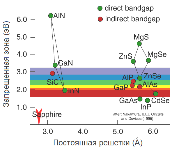
The lattice constant of a semiconductor is laid horizontally here - roughly speaking, the distance between two neighboring atoms in a crystal (we will return to it later). Vertically - the width of the forbidden zone in electron-volts (eV). To have an idea, a person sees photons with energy from 1.8 eV (wavelength 700 nm, red color) to 3.1 eV (400 nm, purple). We are interested in the blue-violet region, with a margin of about 2.6–3.3 eV.
Lyrical digression: electron volts
According to the definition, energy of 1 eV is enough to reduce the potential of an electron by 1 volt. And vice versa: if we increase the potential of an electron by 1 Volt (say, after it runs from “-” to “+” of a single-volt battery), then it will receive energy of 1 eV. Thus, if the band gap of a semiconductor is 3 eV (purple LEDs), then in order to throw an electron into the conduction band, its potential can be increased by 3 V. In general terms, this determines the operating voltage across the LED, reaching as much as 3–3.5 V for blue / violet diodes.
As we see, only three semiconductors fall into the blue-violet region: SiC, ZnSe, and GaN. Historically, in this order, they went to the "LED" arena.
1. Silicon carbide (SiC)
Silicon carbide is remarkable for being able to form a huge amount of crystalline modifications. Already in the 50s, this allowed the creation of structures with different widths of the forbidden zone - and therefore, to generate radiation in different parts of the visible spectrum. After the red and yellow LEDs, the first blue LED was developed in 1969. In the 80s they became commercially available.
However, with all the technological advances, the efficiency of the devices did not exceed 0.03%. The reason was fundamental. To understand it, we will have to delve a bit into physics.
Direct and indirect semiconductors
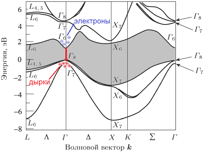
In fact, the band structure of a semiconductor looks a bit more complicated than in the figure above. The position of the zones (and the width of the forbidden zone) depends on the electron momentum in the crystal (that is, in fact, on its velocity). Moreover, it depends on the vector: not only on the magnitude, but also on the direction. The result is something like this:
Source: [1]
This is the band structure of gallium arsenide. Vertically traditionally deposited energy. Horizontal - without going into details - different possible values of the vector impulse (also called the wave vector or the position of the electron in the Brillouin zone ) are shown. For example, electrons in a gamma point (any of the letters D in the picture) have zero momentum. For clarity, I painted the forbidden zone gray. Now we look at the red arrow: an electron from the lowest point of the conduction band falls to the highest point of the valence band without changing the momentum (the same horizontal coordinate), emitting a photon. This is a direct transition.
And what happens in SiC?
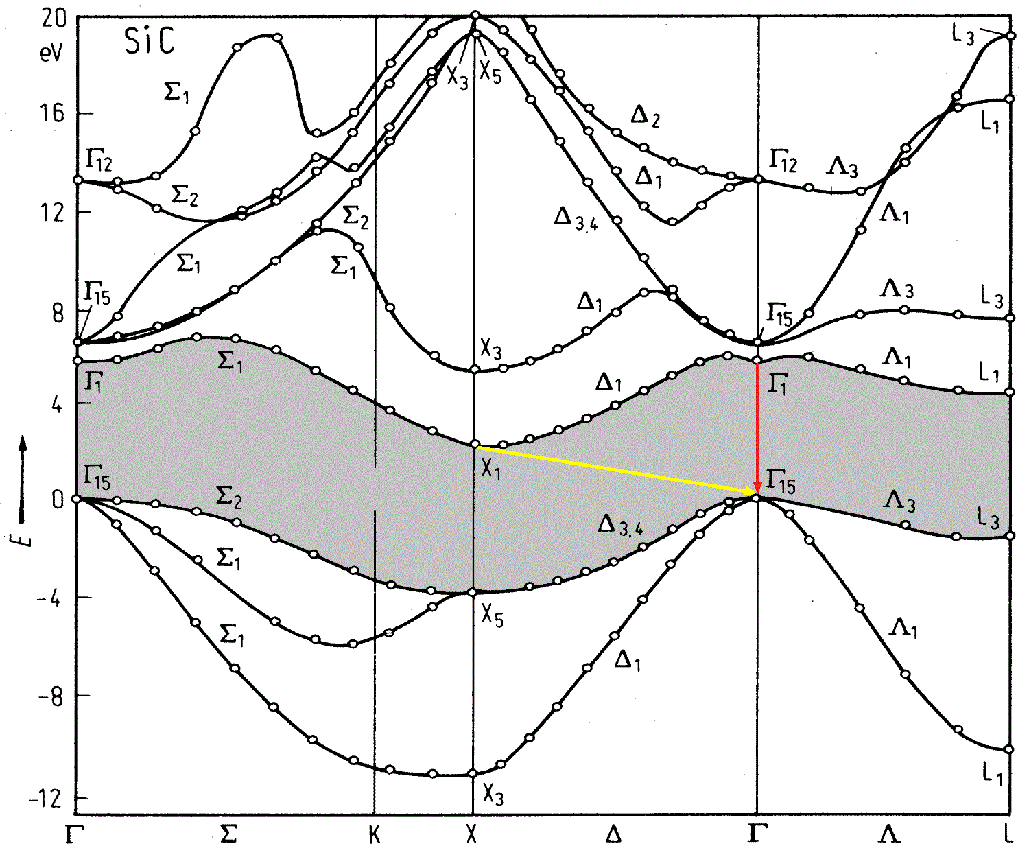
A source
We look at the yellow arrow. Electrons from the lowest point do not fall vertically down, but at an angle ( indirect transition) - which means they change their momentum. The problem is that for the emitted photon this impulse is too large, and the law of conservation of impulse has not been canceled. One more particle is needed — the phonon — capable of compensating for the electron momentum. True, now our process of two-particle (electron-photon) has become three-particle, which significantly reduced its probability. For the LED, this means that of all the electrons in the conduction band, only a few will be able to emit a photon - which means we will noticeably lose in efficiency.
Question: is the red arrow in the picture, is it okay with it?
Answer: Yes, the transition is direct, but its energy is almost 6 eV (good ultraviolet, you can burn your eyes). For us, this is overkill.
Actually, it is the indirect transition of SiC that predetermined its fate (or rather, its ending) in optoelectronics. Fortunately, ZnSe and GaN turned out to be direct-gap semiconductors.
2. Zinc selenide (ZnSe)
ZnSe differed from SiC not only in
First, there was a problem with the manufacture of contacts to the diode. The contacts must be metallic, and a Schottky barrier inevitably forms at the metal-semiconductor interface. The trouble with ZnSe was that a huge voltage drop was observed on the Schottky barrier. As a result, the operating voltage of the diode reached 10 V instead of the expected 2.8. Later it was reduced to 4.2 V, and then only at the price of a noticeable complication of production.
The next problem turned out to be a heat sink. Low electron mobility in ZnSe leads to high resistance (and, as a result, large heat release); low thermal conductivity makes the situation worse.
Finally, the most serious obstacle was the degradation of the material in the process. The essence of this process is reduced to a sharp increase in the number of defects in a crystal at high current or radiation densities. This wildly reduced the lifetime of the device (in general, it is difficult to talk about the “lifetime” when the laser diode burns out after 20 seconds of operation).
Thus, only low-power blue diodes became the lot of zinc selenide. Another material remained in the reserve, in the possibility of which very few people believed at first.
3. Gallium nitride (GaN) and other III-nitrides
To understand why the GaN diodes were returned only in the mid-80s, we need to remember how LEDs are generally produced. Thin layers of semiconductors (in fact, all electronics are more complicated than a transistor) are grown by epitaxial methods. The essence of this word lies in the fact that we are besieging atoms on the surface of a semiconductor, which lie not in an inconsistent manner, but in a quite orderly way - repeating and continuing the crystal lattice, as it were. (This is simply energetically beneficial.) As a result, layer by layer, we get an almost perfect crystal.

A source
The subtlety here is that we cannot start epitaxy from scratch. You need an initial single crystal - substrate .
Lyrical digression: the growth of substrates
Probably many of the readers of Hicktimes raised salt crystals in their childhood. It was necessary to tie a thread with a seed - a grain of salt - and hang it in a saline solution. So, single crystals of semiconductors grow about the same - of course, from the components of the highest purity, while still rotating the seed and slowly pulling it up. This is called the Czochralski method . The grown cylinder is cut into thin plates - future substrates, then they are polished, packed in special clean containers and sent for production.

Sources: 1 , 2 .
Sources: 1 , 2 .
The rest is simple: we take a silicon carbide substrate, with an epitaxy we grow a silicon carbide diode on it. Although there will be a problem with ZnSe: ZnSe substrates are not widely manufactured. Then let's take a GaAs substrate: judging by the “world map”, the lattice constants of GaAs and ZnSe are almost the same (5.66 Å), so the growth will go well. The problem would be if we took a silicon carbide substrate with a lattice constant of about 3 Å: ZnSe could not repeat such a tight lattice due to internal stresses (in fact, repulsion between the Zn and Se atoms). Even on silicon (5.4 Å, the difference is only 5%) it would be problematic to grow ZnSe - starting from a certain layer, the internal stress in the ZnSe layer would become too great, and he would want to grow from his usual lattice constant. The transition from one grid to another would look something like this:

A source
That is, the inconsistency of the lattices leads to the appearance of such defects. And defects in optoelectronics are very bad. Moral: choose the right substrate for epitaxy!
Solid solutions
Take a ZnSe crystal and replace all zinc atoms with magnesium atoms. The result is a MgSe crystal, which has slightly different lattice constant (magnesium atom is larger than zinc atom) and the band gap. And what if not all atoms are replaced, but only some? Say, five percent? Something intermediate will turn out: the lattice form will remain the same, but the lattice constant and the band gap will be somewhere between them for ZnSe and MgSe. Such a substance is called a solid solution of ZnSe and MgSe, denoted as Zn 0.95 Mg 0.05 Se and on the "world map" lies on the straight line connecting ZnSe and MgSe.

Actually, the lines on the "world map" show for which pairs of semiconductors there are stable solid solutions. Thus, by controlling the concentrations of the components during growth, we can adjust the lattice constant and the band gap of the semiconductor - and therefore control the radiation wavelength. Thus, the addition of indium to GaN allows the transition from ultraviolet (3.4 eV) to the visible blue region (2.7–2.9 eV).
Backing for GaN
Now it’s clear what the value of the “world map” is: it allows you to select solid solutions for controlling the wavelength and the corresponding materials for the substrate. Well, let's pick up the substrate for InGaN growth (it so happened that it is impossible to grow GaN substrates). Wait, how is it - no suitable substrates? Not at all?

SiC is close, but is not optimal (the difference between the permanent gratings is 4%) and, besides, is expensive. Because of the price, sapphire was mainly used.
Actually, the lack of substrates was the reason why in the 80s everyone worked with zinc selenide. It was believed that the quality of growth should be a major success factor. The only exception was the Isamu Akasaki group at Nagoya University. By 1986, they offered a clever solution to the problem. The bottom line was that several intermediate (so-called buffer ) GaN layers were grown on a sapphire substrate. The concentration of defects in them was huge, but decreased from layer to layer. Later, Shuji Nakamura (Nichia Corp.) refined this process using AlGaN buffers. It turned out this structure:

A source
In an electron microscope, it looked like this:

On the left - GaN on sapphire, on the right for comparison ZnSe on GaAs (the GaAs substrate is not shown, but judging by the size it is not far). Pay attention to the scale: GaN is one and a half times thicker. Sources: 1 , 2 .
So, even after all the improvements, the dislocation density remained huge. And defects for optoelectronics are not just bad, but very bad: they capture media and allow them to recombine nonradiatively, drastically reducing efficiency. This is the difference between the diode and the LED: making a pn junction is not a problem, making a defect free pn junction is a complex technological task. For example, a GaAs LED with a concentration of defects like in the picture would obviously not work (or rather, it would, but at best, just a diode).
Here nature intervened: it turned out that the quality obtained is sufficient for normal operation of the LEDs. The reasons for this are extremely nontrivial and not studied until the end. One of them is not quite the usual mobility of carriers in GaN: they do not move over long distances, and therefore can avoid meeting with the dislocation. Moreover, almost all dislocations in GaN are filiform, extending from the substrate to the diode surface itself. This imposes some restrictions on their properties that can be used in practice.
Unbelievable, but true: the biggest problem of gallium nitride was suddenly behind.
GaN Acceptors
Another difficulty was the p-doping of gallium nitride. In the early stages, magnesium was used as an acceptor (material for p-doping). However, the resulting material did not behave like a p-type semiconductor. There was some unknown factor that prevented magnesium from playing the role of an acceptor.
The easiest way to determine the degree of doping is to measure the resistance of the material. In p- and n-doped semiconductors, it is low due to an excess of carriers (electrons in n-or holes in the p-type). In a pure semiconductor there are no free carriers, therefore its resistance is high.
Remarkable next episode. Akasaki was able to show that irradiation of GaN with a low-energy electron beam solves the problem: magnesium began to behave as an acceptor. However, in the production process, the material again ceased to be conductive. It happened during annealing : the structure was kept at a high temperature in ammonia. This is a standard procedure to reduce the stresses in the crystal lattice.
Nakamura noticed that p-conductivity disappears at an annealing temperature above 400 ° C. At the same temperature, the dissociation of ammonia into nitrogen and hydrogen begins. And what if the problem is somehow related to hydrogen? Detailed studies have shown that Nakamura was right: atomic hydrogen penetrated into the structure, contacted magnesium and shared its electron with it, preventing it from playing the role of an acceptor. Annealing in nitrogen instead of ammonia immediately solved the problem:

Upper curve: when annealing in ammonia above 400 ° C, the resistance of the material increases dramatically. In nitrogen (bottom line) this does not happen. A source.
Later it turned out that annealing in nitrogen does not just solve the problem with ammonia - it can completely replace the electron beam. That is, instead of what Akasaki did, you can simply anchor the material in nitrogen: this will destroy the bonds of magnesium with hydrogen and make the material p-conductive. Technologically, this was extremely important: the treatment of large crystals with an electron beam is not a quick and expensive thing.
Happy end

Shuji Nakamura. A source.
The story did not end there, but the main problems were solved. Along the way, we managed to make a lot of interesting things, for example, to develop a special reactor for the growth of III-nitrides. By 1994, Nichia Corp. Began industrial production of blue InGaN LEDs.
Sources
[1] P. Yu, M. Cardona, Fundamentals of Physics of Semiconductors - Moscow: Fizmatlit, 2002. - 560 p.
[2] S. Nakamura, S. Pearton, G. Fasol “The Blue Laser Diode: The Complete Story” - Springer, 2000. - 368 p.
[3] H. Morkoç et al. J. Appl. Phys. 76, 1363 (1994).
[4] http://www.eurotechnology.com/store/solidstatelighting/
[5] http://www.nobelprize.org/nobel_prizes/physics/laureates/2014/ (the title picture is also from here)
UPD. Thanks to Mercury13 and jar_ohty for comments on ammonia.
Source: https://habr.com/ru/post/364387/
All Articles