Intel promises 10 TB SSDs in two years
256–384 gigabit on a 32-layer 3D chip
 In conventional NAND memory, electrical elements are combined within planar structures, and the layers are not interconnected. In August last year, Samsung began to produce V-NAND chips, consisting of vertically stacked 24 and later 32 layers of cells. For a long time, only a Korean company released a 3D memory, but on November 20 of this year, Intel revealed plans for a response decision in a video presentation for investors .
Intel is going to fit 256 gigabytes (32 gigabytes) on a single NAND memory chip of 32 layers using MLC technology (multi-level cell), using which two bits are stored in each cell, which requires calibration of four states. When using TLC (triple-level cell, eight states), this volume will increase one and a half times to 384 gigabytes (48 gigabytes).
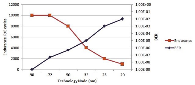
Samsung is working on 14nm “flat” circuits. Intel and Micron are working on a 16 nm 2D process memory. But the reliability of 3D-memory decreases with decreasing element sizes. Samsung 3D chips use 40nm process technology, and Intel is expected to do the same.
')
Increasing the size of elements using 3D-technology has led to the fact that the Samsung 850 Pro is called the fastest and most reliable drive on the market.
Intel would not like to set a rigid framework of the moment of the emergence of 10-terabyte hardcore. Most likely , a device of this size will first be aimed at the corporate sector and only later will be widely used in home computers.
Intel vice president and CEO Rob Kruk promised that the first drives of this size will be created in two years. As he noted, a terabyte memory thickness of 2 mm is possible, which means that the memory capacity of mobile devices will also increase.
The new chips will be produced in collaboration with Micron Technology at the Intel Micron Flash Technologies plant in Lehi, Utah. The start of work is scheduled for the second half of 2015.
For comparison : the Samsung has a V-NAND SM1715 NVMe drive with a capacity of 3.2 TB. The 400GB 845DC Pro uses 4 24-layer 3D chips with a 40 nm process, each 128 GB. In the model 850 Pro used 32-layer V-NAND MLC-chips with a volume of 86 gigabits.
At the end of this year, Hynix plans to begin production of 3D-NAND. Similar work is underway in SanDisk, perhaps in 2015 we will see their first results on the shelves. It is likely that next year 3D-memory will become the norm.
Source: https://habr.com/ru/post/363485/
All Articles