Russian production of embedded systems
This post will be interesting for those who want to see what Russian high-tech electronic equipment looks like, namely embedded systems.
For those who do not know what embedded systems are, in simple words - these are processor boards and peripheral modules of various formats, for example, CompactPCI, PC / 104, MicroPC, which are built into various systems: from industrial automation to telecommunications equipment.
')
For those who know all this - do not take it personally.
Immediately make a reservation that I am not an employee of this plant, so many things happening there will remain a secret for me.
Against the background of the growing Russian fables, one can doubt the existence of high-tech production in the territory of the Russian Federation. But it exists! And when I had the opportunity to go to the factory - I, of course, went there with great interest. I will try to share what I saw there.
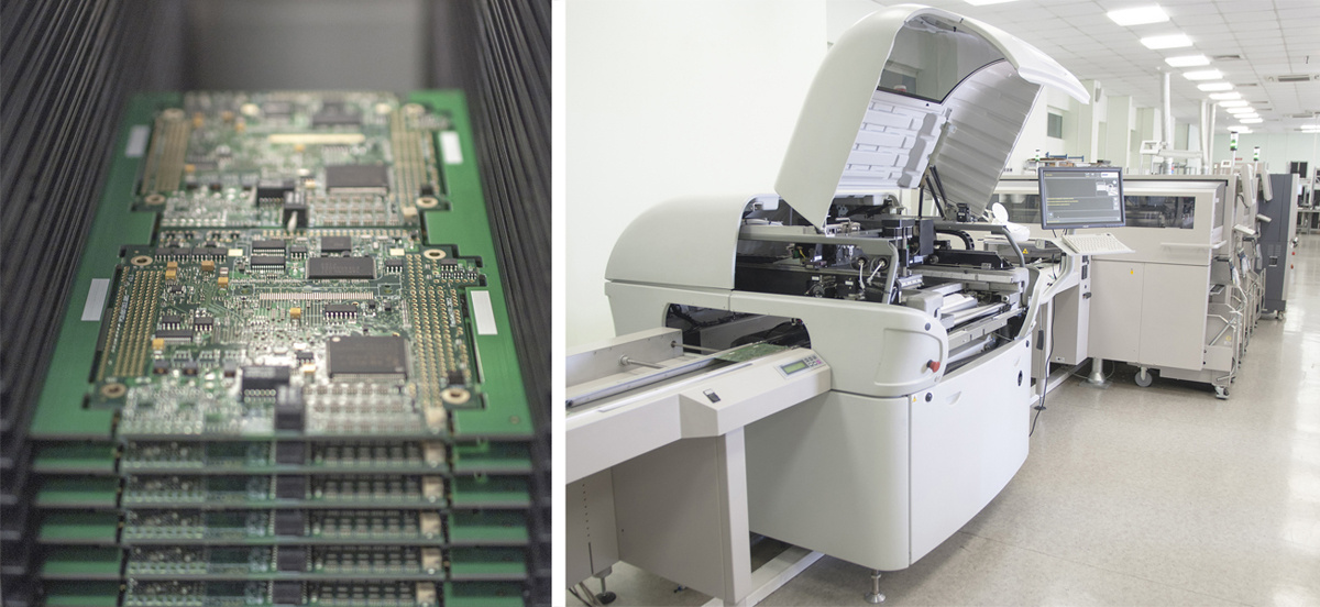
All production is distributed in several geographical points of Moscow. I visited the largest object. It is located on the territory of Moscow, even inside the Moscow Ring Road, and occupies almost the entire floor of the building of the scientific research institute. There are several premises here: a workshop where there are production lines, a manual assembly workshop, warehouses, as well as various administrative premises.
To get to the plant, you need to go through a fairly serious access system. And then go along the underground corridors that unite several tall buildings among themselves. If there were no conductor, we would definitely get lost.
The production maintains a certain level of cleanliness and order. There are no clean rooms here, but nevertheless all employees go in bathrobes and rubber slaps. As they explained to us, slaps are not a fad, but additional protection against electrostatics. By the way, the factory is not at all noisy.
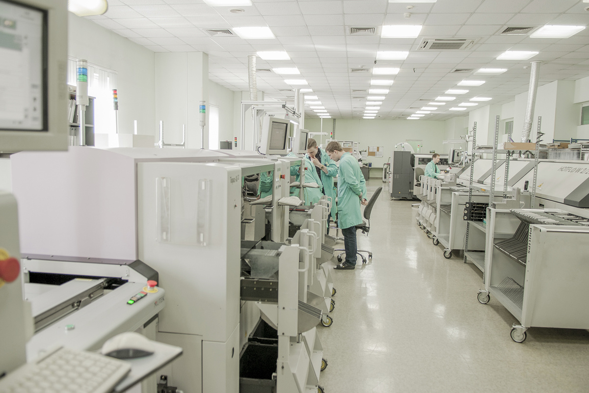
Figure 1. Main workshop with production lines

Figure 2. View of the shop in the other direction
Initially, the boards are designed. The developers in the design center are responsible for this. This time I will not talk about them. After all, the most interesting things happen in the developer’s head, and it’s hard to get there. Therefore, let's see what happens after everything is invented.
The life of the board at the factory begins with such blanks that are made in advance. By the way, in the photo there are blanks for PC / 104-Plus format boards (this is evident from the presence of ISA and PCI bus contacts).
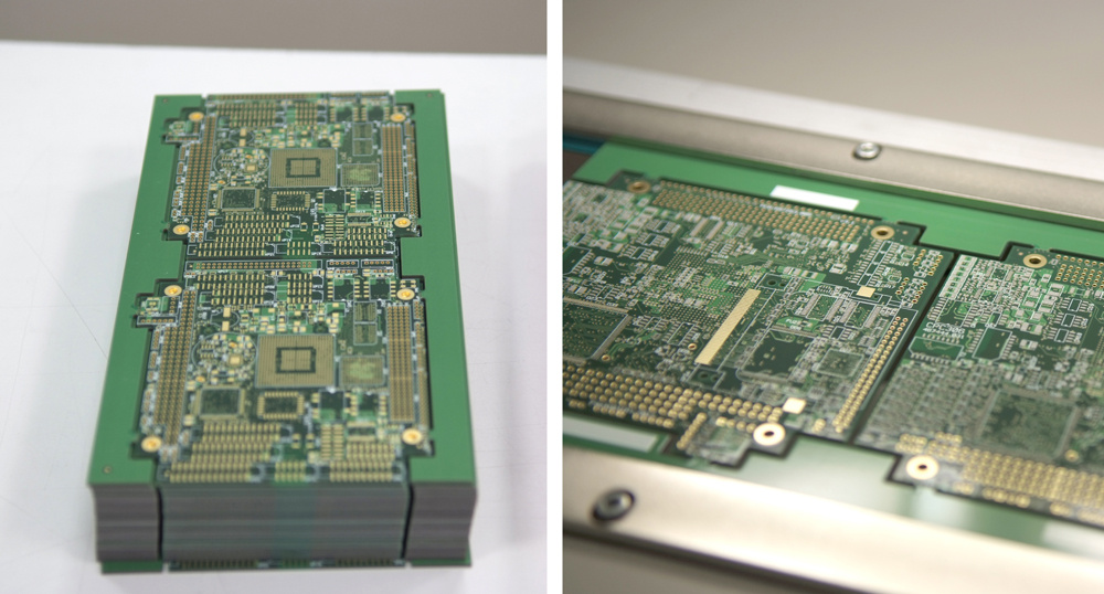
Figure 3. Blanks. No components yet
The blanks are fed to the production line in the screen printing printer, where the solder paste is applied to the required sites - to the places where the so-called SMD components will be installed. Solder paste provides electrical contact and mounting components.
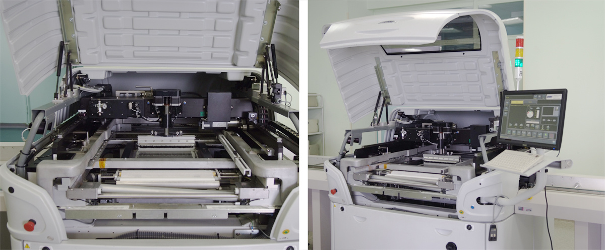
Figure 4. Screen printing printer
The paste is viscous and probably sticky. Probably, because although there was an opportunity to poke a finger at her, the natural modesty and the fear of spoiling everything prevented it.
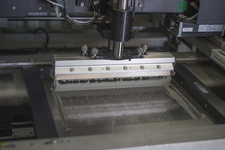
Figure 5. Paste application
After the paste has been applied, the board is moved to the automatic surface mount assembly of the components.
This plant specializes in systems designed for the harsh Russian reality: low temperatures from -40 to 85 ° C, and sometimes lower. Therefore, the components are set appropriate - harsh and brutal. Although outwardly and not tell.
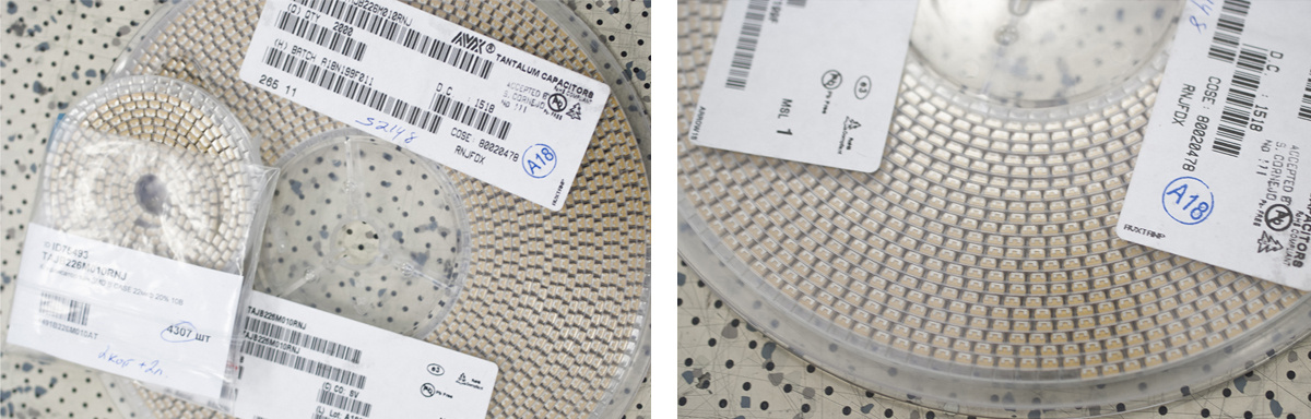
Figure 6. Tantalum capacitors. Solid capacitors, for example, are more reliable at low temperatures than electrolytic
The way I supplied the components for mounting me especially impressed. Not that I thought they were brought dumped in a box. Not that I ever thought about how components are installed on the board! But the fact that they are served in ribbons became for me a revelation from the category: “Aah, that’s how it is!”. Convenient and practical. And if components run out in some tape, the operator is notified.
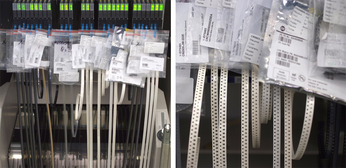
Figure 7. Here is the revelation!
As I have already said, the boards with the paste applied are transferred further to the automatic installer of the components.

Figure 8. Automatic component installer
This illustration shows the interior of the apparatus that installs the components.
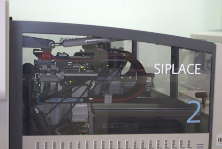
Figure 9. Insides
But looking at the photo is not as interesting as gif-ku. They say that if you look at it long enough you can achieve technical enlightenment.
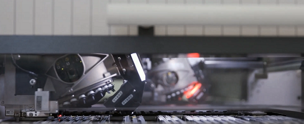
Figure 10. Click to open gif (carefully, ~ 18Mb)
For the installation of large components using selective soldering. In this process, there are several steps: applying flux to the bottom surface of the board, preheating the board and components, and soldering itself.
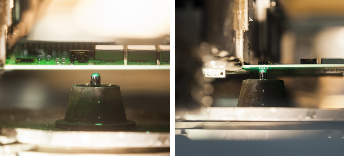
Figure 11. Selective component soldering
Next - the boards pass through a convection convection oven for soldering other components.
Unfortunately, we did not have a full tour of the plant. It was also inconvenient to divert specialists from their work on stupid questions. Therefore, many things had to be thought out, such as, for example, what is depicted in the mnemonic diagram on the right (Fig. 12).
But we were lucky - one specialist from the workshop heard our reasoning and confirmed: on the screen is a zonal profile of the temperature distribution inside the furnace.

Figure 12. The verb anneal gains new meanings
After the boards have been fired, they are washed away from any dirt and solder residue. Yes, yes, in Russia not only money can be laundered!
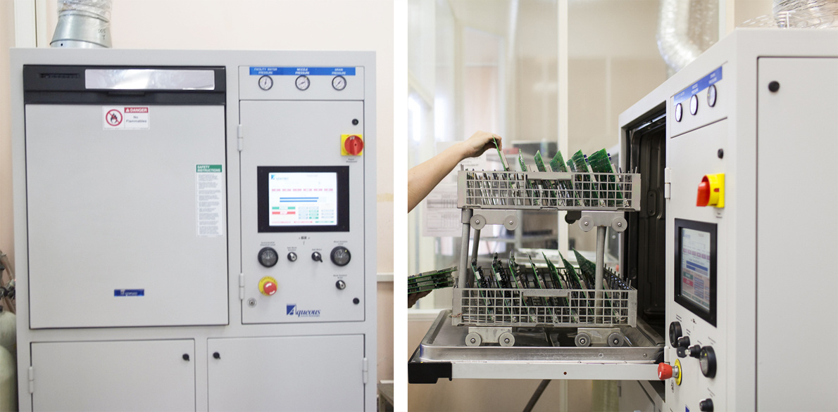
Figure 13. Washing and Drying Boards
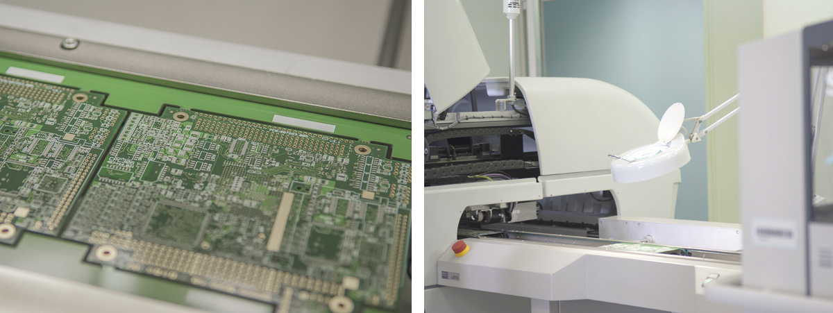
Launched fees are sent to the control. Several control methods are used. With automatic visual inspection, the board is placed in the device, where the ISP is used in the device, and the board image is obtained, which is automatically compared with the standard.
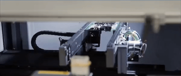
Figure 14. Optical inspection: scanning
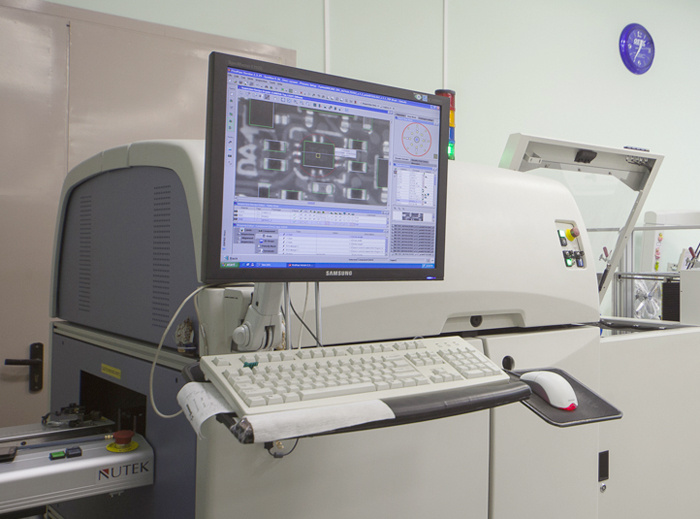
Figure 15. Optical inspection: reconciliation
There is an x-ray control to check the quality of component soldering and assembly control.
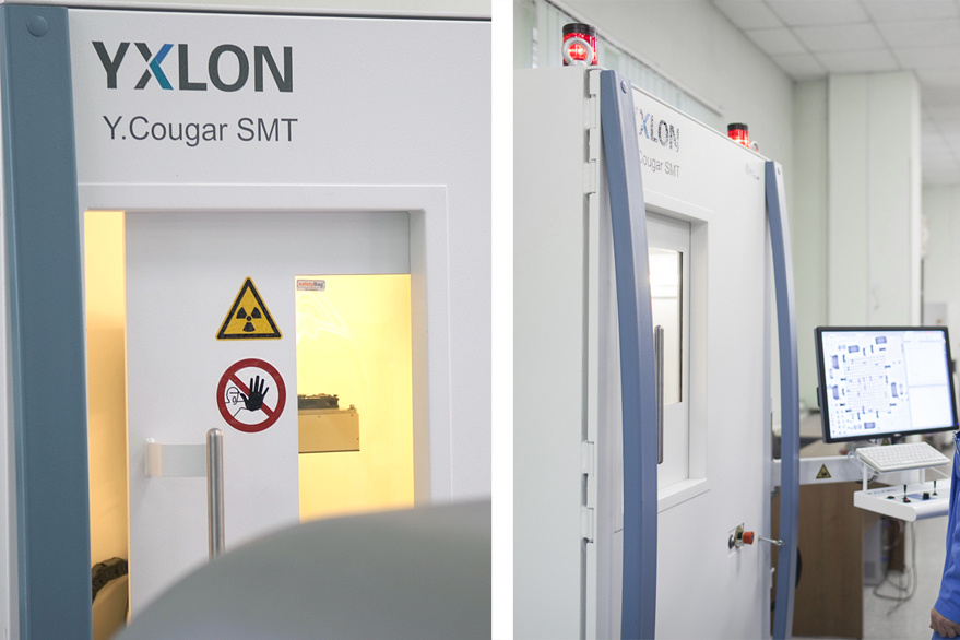
Figure 16. One of the X-ray apparatus
And, of course, here is the usual visual inspection at all stages of production.
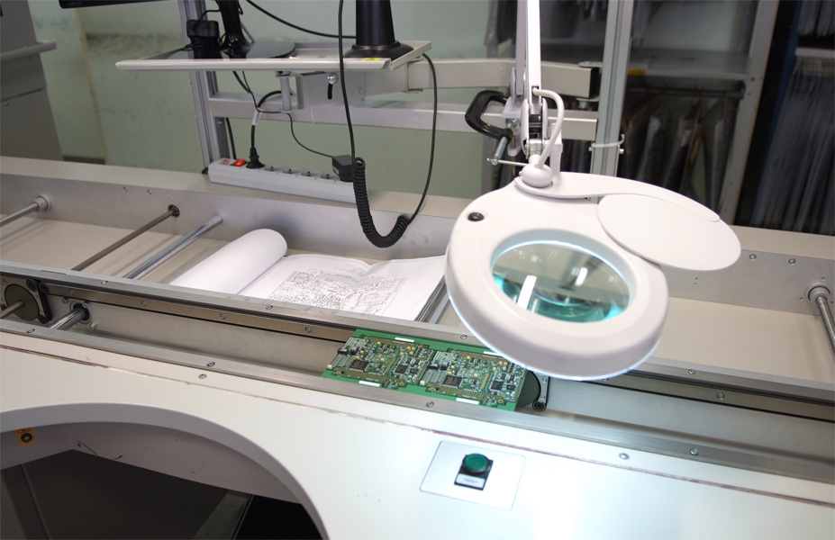
Figure 17. Visual inspection
In the next room, everything is much more interesting - this is a hall for manual assembly and soldering of non-standard components.
In this room, I felt pride in the weaker sex, because half of the “solders” are very pretty girls. To be honest, not surprising. How does soldering differ from cross-stitching? Careful and creative work according to the previously specified pattern. So, forget about the picture, walking on the Internet, where the girl holds her fingers over the hot part of the soldering iron.
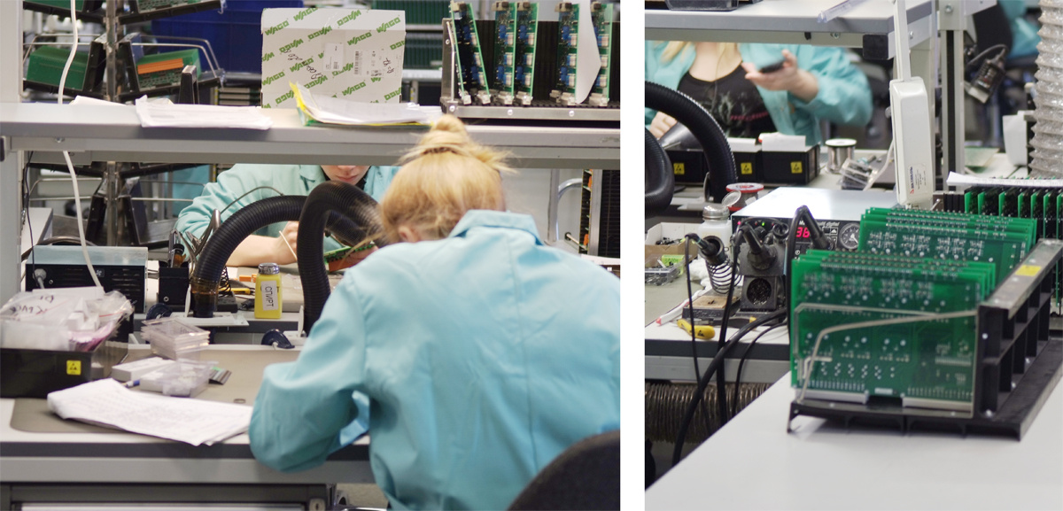
Figure 18. Soldering
After all components are installed, the contacts and connectors are pasted over with a special tape, and the boards are passed on to apply a protective layer. The protective coating is applied under special UV lamps, which allows you to see which areas are not painted.
Rusinok 19. Under the rays of a UV lamp
Born boards are collected and transported to another location, where they pass mechanical and temperature testing, filling and testing software, as well as mounting into the case, if required.
I could sum up my story with some pathos words about Russian production. But honestly, I, as an ordinary engineer, just got aesthetic pleasure from a walk through the plant.
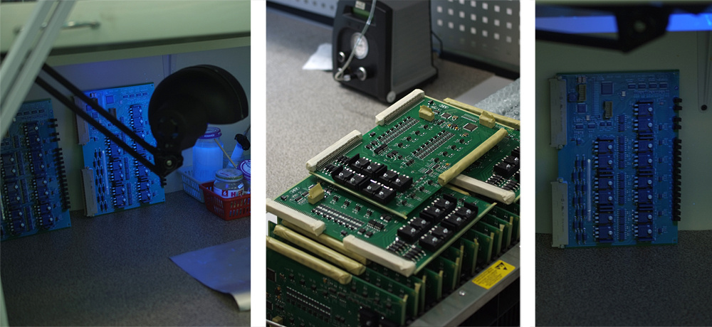
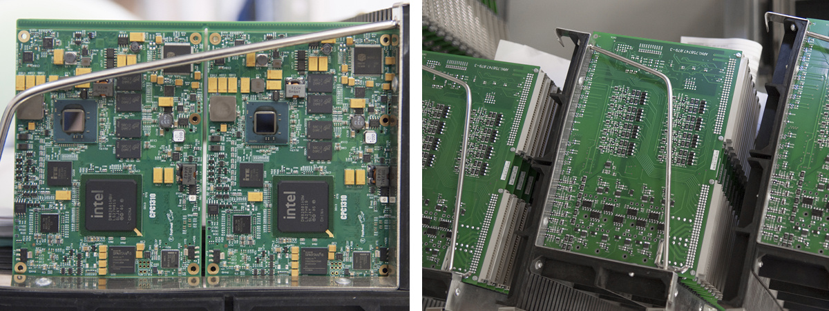
Finally, several photos that are not included in any section.

Thanks for attention!
For those who do not know what embedded systems are, in simple words - these are processor boards and peripheral modules of various formats, for example, CompactPCI, PC / 104, MicroPC, which are built into various systems: from industrial automation to telecommunications equipment.
')
For those who know all this - do not take it personally.
Immediately make a reservation that I am not an employee of this plant, so many things happening there will remain a secret for me.
It exists!
Against the background of the growing Russian fables, one can doubt the existence of high-tech production in the territory of the Russian Federation. But it exists! And when I had the opportunity to go to the factory - I, of course, went there with great interest. I will try to share what I saw there.
All production is distributed in several geographical points of Moscow. I visited the largest object. It is located on the territory of Moscow, even inside the Moscow Ring Road, and occupies almost the entire floor of the building of the scientific research institute. There are several premises here: a workshop where there are production lines, a manual assembly workshop, warehouses, as well as various administrative premises.
To get to the plant, you need to go through a fairly serious access system. And then go along the underground corridors that unite several tall buildings among themselves. If there were no conductor, we would definitely get lost.
The production maintains a certain level of cleanliness and order. There are no clean rooms here, but nevertheless all employees go in bathrobes and rubber slaps. As they explained to us, slaps are not a fad, but additional protection against electrostatics. By the way, the factory is not at all noisy.
Figure 1. Main workshop with production lines
Figure 2. View of the shop in the other direction
How to start the board
Initially, the boards are designed. The developers in the design center are responsible for this. This time I will not talk about them. After all, the most interesting things happen in the developer’s head, and it’s hard to get there. Therefore, let's see what happens after everything is invented.
The life of the board at the factory begins with such blanks that are made in advance. By the way, in the photo there are blanks for PC / 104-Plus format boards (this is evident from the presence of ISA and PCI bus contacts).
Figure 3. Blanks. No components yet
The blanks are fed to the production line in the screen printing printer, where the solder paste is applied to the required sites - to the places where the so-called SMD components will be installed. Solder paste provides electrical contact and mounting components.
Figure 4. Screen printing printer
The paste is viscous and probably sticky. Probably, because although there was an opportunity to poke a finger at her, the natural modesty and the fear of spoiling everything prevented it.
Figure 5. Paste application
After the paste has been applied, the board is moved to the automatic surface mount assembly of the components.
Severe components
This plant specializes in systems designed for the harsh Russian reality: low temperatures from -40 to 85 ° C, and sometimes lower. Therefore, the components are set appropriate - harsh and brutal. Although outwardly and not tell.
Figure 6. Tantalum capacitors. Solid capacitors, for example, are more reliable at low temperatures than electrolytic
The way I supplied the components for mounting me especially impressed. Not that I thought they were brought dumped in a box. Not that I ever thought about how components are installed on the board! But the fact that they are served in ribbons became for me a revelation from the category: “Aah, that’s how it is!”. Convenient and practical. And if components run out in some tape, the operator is notified.
Figure 7. Here is the revelation!
As I have already said, the boards with the paste applied are transferred further to the automatic installer of the components.
Figure 8. Automatic component installer
This illustration shows the interior of the apparatus that installs the components.
Figure 9. Insides
But looking at the photo is not as interesting as gif-ku. They say that if you look at it long enough you can achieve technical enlightenment.
Figure 10. Click to open gif (carefully, ~ 18Mb)
How to properly anneal
For the installation of large components using selective soldering. In this process, there are several steps: applying flux to the bottom surface of the board, preheating the board and components, and soldering itself.
Figure 11. Selective component soldering
Next - the boards pass through a convection convection oven for soldering other components.
Unfortunately, we did not have a full tour of the plant. It was also inconvenient to divert specialists from their work on stupid questions. Therefore, many things had to be thought out, such as, for example, what is depicted in the mnemonic diagram on the right (Fig. 12).
But we were lucky - one specialist from the workshop heard our reasoning and confirmed: on the screen is a zonal profile of the temperature distribution inside the furnace.
Figure 12. The verb anneal gains new meanings
After the boards have been fired, they are washed away from any dirt and solder residue. Yes, yes, in Russia not only money can be laundered!
Figure 13. Washing and Drying Boards
Full control and domination
Launched fees are sent to the control. Several control methods are used. With automatic visual inspection, the board is placed in the device, where the ISP is used in the device, and the board image is obtained, which is automatically compared with the standard.
Figure 14. Optical inspection: scanning
Figure 15. Optical inspection: reconciliation
There is an x-ray control to check the quality of component soldering and assembly control.
Figure 16. One of the X-ray apparatus
And, of course, here is the usual visual inspection at all stages of production.
Figure 17. Visual inspection
Soldering
In the next room, everything is much more interesting - this is a hall for manual assembly and soldering of non-standard components.
In this room, I felt pride in the weaker sex, because half of the “solders” are very pretty girls. To be honest, not surprising. How does soldering differ from cross-stitching? Careful and creative work according to the previously specified pattern. So, forget about the picture, walking on the Internet, where the girl holds her fingers over the hot part of the soldering iron.
Figure 18. Soldering
Level 80 Protection
After all components are installed, the contacts and connectors are pasted over with a special tape, and the boards are passed on to apply a protective layer. The protective coating is applied under special UV lamps, which allows you to see which areas are not painted.
Rusinok 19. Under the rays of a UV lamp
Born boards are collected and transported to another location, where they pass mechanical and temperature testing, filling and testing software, as well as mounting into the case, if required.
That's all
I could sum up my story with some pathos words about Russian production. But honestly, I, as an ordinary engineer, just got aesthetic pleasure from a walk through the plant.
Finally, several photos that are not included in any section.
Thanks for attention!
Source: https://habr.com/ru/post/358340/
All Articles