Indication of output parameters and implementation of load protection in the UPS. Part 4.1
Part 1
Part 2
Part 3
Good day to all and this is the last part of the cycle dedicated to the non- power part of the device. Perhaps you will think that I deliberately tighten the power modules, but this is not so. I just would like to finish with all the side modules that are partly "decorative", but without which our UPS turns into a pile of poorly working iron with an incomprehensible purpose.
Therefore, this article will discuss in detail the implementation of the measurement of voltages, currents in the nodes, as well as temperature control and protection from overheating. And of course - an indication of where we are without it! Indeed, without it, it is quite problematic to understand what is going on with our device, how well it works and whether it works at all.
A few more statements before the start:
1) In the industrial version, the board was divorced in 4 layers for the implementation of high-quality trace of the board, with galvanic isolation and minimal noise, but in this article I will give two types of trace and both for "radio amateurs"! One view is a double-sided board, the other option is one-sided. I can immediately note that even these options have more than enough noise properties for reliable operation, and the galvanic isolation has been removed to reduce the cost of manufacturing, because This node is not responsible and in the event of a malfunction, the device will continue to operate and signal an incident that has occurred.
Of course, before putting them into the article, I made a prototype, hard I drove it and appreciated more than suitable survivability. I also checked the possibility of making these boards with the help of LUT and photoresist - a step of 0.3 mm is achieved without problems.
')
2) Anyone who wants to repeat this unit or the entire UPS, I am ready to send the programmed STM32 microcontroller if its presence scares you away. The price will be: the cost of MK + shipping, solely for the purpose of helping, and not making money.
Some clarity seemed to have introduced, then we went to understand the scheme ...
And so the general scheme of the module that will be discussed today, rewritten it specifically for this article on modules, so that newbies find it easier to understand the general principle of operation and what “piece” is responsible for what in the final functional:
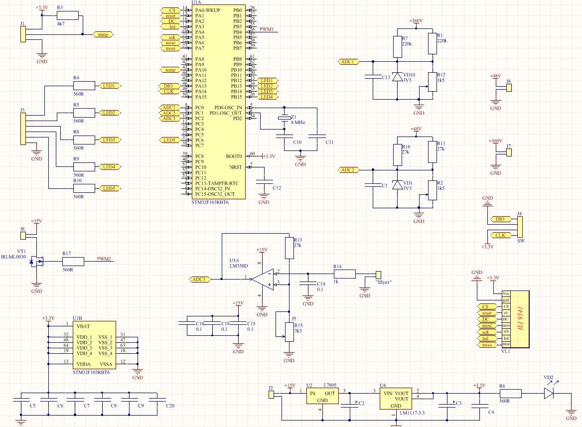
Figure 1 - Schematic diagram of the display and control unit on the STM32F103RBT6
1) the first thing is striking "rectangle" with the inscription ILI9341. This is a color TFT screen with a resolution of 240x320 pixels and a diagonal of 2.4 ". Almost all the information about the measurements will be displayed on it.
2) we also see an inscription near one of the “Shunt” connectors, which I think suggests measuring the current with good accuracy. This is exactly what justifies the use of a current shunt in this circuit, and not a current transformer. The latter are used in power modules for protection against short circuits (short-circuit)
3) we also see a pair of connectors labeled "+ 360V" and "+ 48V" - this is monitoring the voltage on the DC bus (including the battery) and measuring the output voltage. Simply, to reduce the time constant of the circuit, it was decided to carry out measurements in a high-voltage DC circuit, since the output voltage (AC) linearly depends on it, so it is not difficult to recalculate the constant to alternating voltage at the output of the UPS
4) those who worked with the DS18B20 sensor will immediately pay attention to the J1 connector; this is where we will connect our thermal sensor
5) The sensor is a feedback circuit for cooling coolers that connect to connector J8.
6) there is a magic J3 connector, which has a bunch of identical resistors and LED inscriptions around it, probably everyone guessed that the same LED indication was connecting here that you could see on the front panel of the UPS
The general possibilities of the scheme were discussed, you need to make out how each block works.
1) Let's start with the most important thing - with nutrition, you can't break a diet. If someone suddenly forgot the previous article - the power supply at us has a voltage of 15V, we need to power all our good from this voltage, taking into account that the microcontroller is powered by 3.3V.
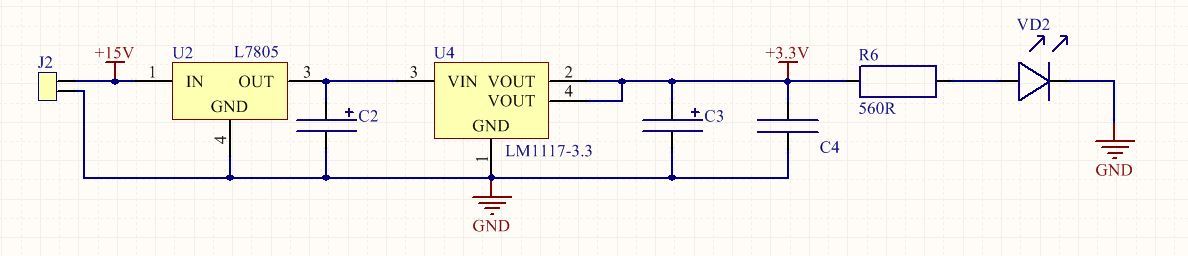
Figure 2 - Supply Stabilization Circuits
Stabilizers are all linear, because The current in the + 3.3V circuit will not exceed 0.25A. There is one fundamental point - the presence of seemingly excess LM7805 stabilizer. In fact, I somehow got into such a situation that my stabilizer on AMS1117-3.3 was burning like a fly, and all because I was used to 7805, 7815 and the like - they have a maximum input voltage of up to 40V. AMS1117 has a maximum input voltage of 12V. Therefore, if we give 15V to it, it will burn so that this does not happen we first reduce our 15V to 5V and then 5V to 3.3V.
It seems to be a trifle, but I, because of inattention and habit, somehow in one project got on a dead STM32F407VET stone and a bunch of SDRAM. LED VD2 - just signals the presence of voltage in the power line.
2) Now we need our stabilized power supply to the MC - we will use the available stone STM32F103RBT6. The reasons for his choice will be in the next paragraph. And so the main rule of wiring - a lot of capacitors in the power supply does not happen. At a minimum, there should be 1 0.1 μF capacitor for each pair of legs V cc - V ss . Of course, the power supply circuit of the analog part of V dda should be diluted differently - there should be a separate electrolyte, a choke ... This is all cool, but for consumer tasks and with not very high accuracy, the usual capacitor like in other circuits will suffice.
An ideal variant of the power scheme can be found in the datasheet on any STM.
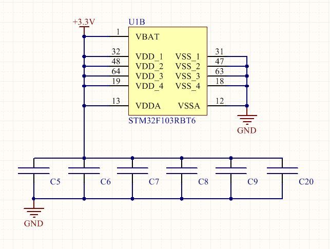
Figure 3 - Microcontroller power circuit
We still see our V bat - it serves to control the power in the line; if it is lowered, it can lead the MK into sleep mode or economy mode. In our problem, this is not relevant, since It is used in systems with battery power, such as a player or phone.
What are capacitors in the circuit for - in order to filter out noise and spikes on the power supply, to eliminate interference. This is especially true for the power supply circuit of the analog part, because measurement accuracy will depend on it.
3) Here I would like to explain why it is STM32F103RBT6. The F10x series is very similar to each other, the first MK that I tried on the ST was the STM32F100RBT6, which stands on the STM32VL-Discovey debug board. It is almost identical to ours and I ran around working with the display on it, but there is one drawback. Our display on ILI9341 works through hardware SPI , which means its speed depends on the frequency of the MK. The F100 is 24 MHz, quite solid, considering the cost at the ATmega8 level, but at this frequency the SPI was not enough to update the image on the TFT with a frequency invisible to the human eye. Therefore, I decided to take a senior friend and the choice fell on the STM32F103RBT6. As I wrote above, the stones are almost the same, the pinout of their legs is the same, roughly speaking - a complete analog. That's just the clock frequency he has already 72 MHz ! Beyond for any AVR-ki and so necessary to us! At such a frequency, the full screen refresh time with a “bare” SPI is 780 ms, which is still noticeable to the eye. Although if you do not update the entire screen, but the inscriptions on it, then nothing is noticeable already. Of course, we don’t need more, but because the project will be open, then maybe someone decides to add the function ofviewing porn branched (tree) menu or something else with a bunch of graphics. Therefore, it was decided to use a very cool part of the periphery - DMA , the work of the SPI + DMA bundle allowed us to reduce the update time to 120 ms, which is enough for excellent work with the graphic menu and other things.
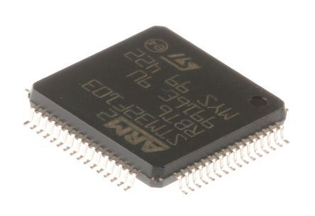
Figure 4 - General view of the STM32F103RBT6 microcontroller in the LQFP-64 package
4) Since our device is a power device and there is something to warm it, it is necessary to implement the temperature control function. It is made on the legendary DS18B20 sensor, which works on the 1-Wire interface “chewed” on the Internet and books. What is he good at? It fulfills our two requirements: it can measure with an accuracy of + -0.5 and is easy to use. In industrial performance, the same sensor is worth it, it's just 3 of them, but this is redundant for the average man, although no one will forbid you to also use 3 of them for each radiator.
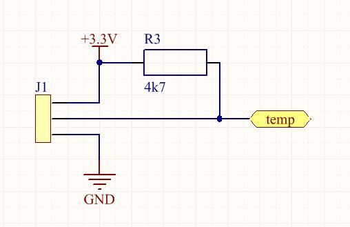
Figure 5 - Connecting a DS18B20 sensor to a microcontroller via a 1-Wire interface
As you can see - everything is so crazy! No difficulties, beyond the wiring requirements of the board and so on. From the diagram it follows that our sensor is connected through the connector, since he himself is attached to the radiators - the main source of heat. The sensor itself is in the TO-92 package. How to work with it programmatically, we will analyze further.
5) The STM32 programming interface is the simplest Serial-Wire interface, which is already made of 3 wires: ground + clock frequency (CLK) + data (DIO).
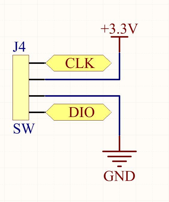
Figure 6 - Microcontroller Programming Interface
I added + 3.3V output to prevent programming the main power supply, but to use the power from the STM32VL-Discovery debug board. I think everything is clear here, just in case I’ll attach a debug photo:
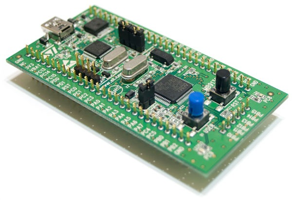
Figure 7 - General view of the STM32VL-Discovery debug board with STM32F100RBT6 stone and ST-link v1.0 programmer on board
If you plan to continue to study my projects and schemes, and there will be a lot of them from welders to HF transceivers , then I strongly advise you to buy a debugging board for you, you can use any fee - according to your budget. If you want cool projects and in-depth research, buy STM32F429-Disco . This fee will cover 95% of your needs, although the price is about 2.5 - 3 thousand rubles.
6) Measurement of operating voltages is implemented on two ADC channels, this STM has 16 such channels, so there are still more possibilities. We are also interested in 2 values : low-voltage DC bus 48V and high-voltage DC bus with 360-400V. Circuitry is the simplest: voltage divider on resistors, one of which is trimmer and voltage adjustment is performed by changing the coefficient. division .
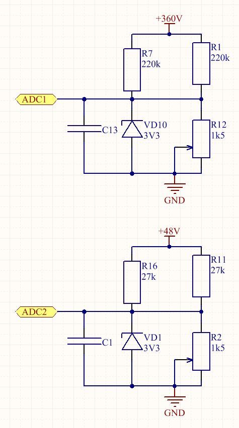
Figure 8 - ADC input circuits for voltage measurement
The formula for calculating the division ratio:
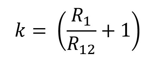
The formula for the dependence of the voltage on the ADC on the input voltage (measured):
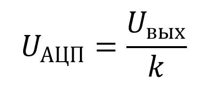
The ADC at STM can measure voltages from 0 to + 3.3V, our task is to choose the coefficient. division so that after the voltage divider 400V and 48V fall into this range. It is desirable that the nominal measured voltage falls approximately at the level of 2V on the ADC, that is, slightly more than the middle. This will measure both smaller and more voltages.
Shunt capacitor - will save us from the pulsations and wrong counting of the ADC, and the Zener diode will protect the input of the ADC MK from overvoltage and ripple, if any.
7) Current measurement is implemented using standard shunts with a nominal drop of 75 mV at 150A . Such a low voltage ADC can measure, but the accuracy and sampling will be low . To solve this problem it is necessary to use an operational amplifier (op amp). It will strengthen us our 75 mV 20 times and we get 1.5V at rated load. Reserve "top" is selected to control the starting and overload currents. After all, we have a stated characteristic of a 200% overload for 20 minutes, and this will create a voltage of 3V on the ADC.
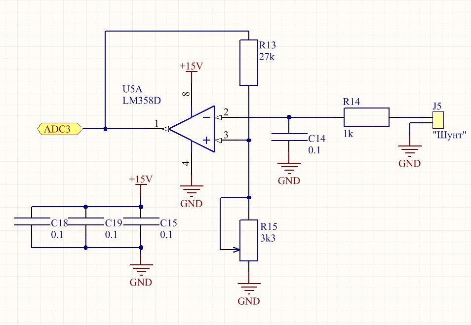
Figure 9 - Implementation of the current measurement circuit at the LM358 op amp
The gain is adjusted by a divider on R13 and R15, by changing it (by adjusting R15 ) we can adjust the current reading. The scheme of inclusion of the OS in general is standard. The only critical moment that arose in my mind is unstable work from + 3.3V. I understand something about this, but in the documentation it was somehow superficially mentioned, I advise you to read the datasheet. Therefore, it was decided to power the DU from + 15V, which we have from duty sources.
8) The last module is the management of the cooling system. It is made on 2 coolers, feedback for their control is performed on the above-mentioned DS18B20. Load control is carried out by power field worker IRLML0030. It is good because it can safely switch the current to 3-4A, and the letter “L” in the markings means that it can work from a low logic level, that is, from + 3.3V. This allows us to directly manage the key from the MC. Controlled rotational speed of coolers using PWM . It is in STM32 hardware, with 4 channels for each timer, and there are many timers ... so there is room for creativity)
I put both coolers on one channel, because it is simply simpler and in this case there is no point in implementing multi-channel control . Feedback "duty cycle - temperature" allows you to maintain the temperature normal to work, as well as to increase (save) the life of the coolers.
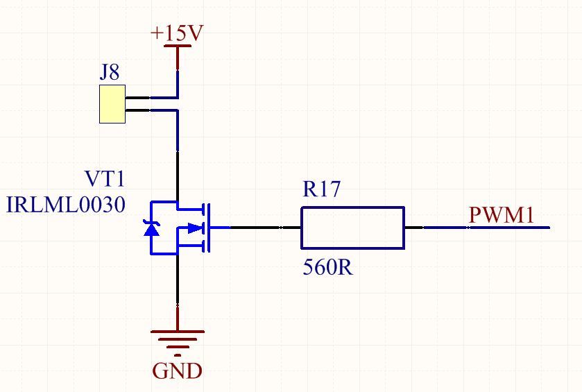
Figure 10 - Scheme of the power circuit control cooler using PWM
Resistor R17 is selected within 100 - 1000 ohms, even though the field-effect transistor opens with voltage and ideally does not consume current, but still its gate has a capacitance. She, in turn, will strive to charge an infinitely large current for an infinitely small time, this is of course all in the ideal model. In reality, the gate capacitance will be charged with a sufficiently large current, and therefore it must be limited so as not to kill the MC. Conclusion STM can give about 10-15 mA or 50-80 mA to the entire port, but the stone is not power, and therefore should not be overloaded. Therefore, we follow the simplest path - we put a current-limiting resistor.
I described its rating above, it is better not to set less than 100 Ohms - the resistor will warm up and the current consumed from the MC will be large. It is not advisable to set more than 1 kΩ. the current will be severely limited, the shutter will charge for a long time and the shape of the PWM will be distorted, and this is not very good. I hope this moment I have explained in some detail.
Option of manufacturing a two-sided board for LUT:
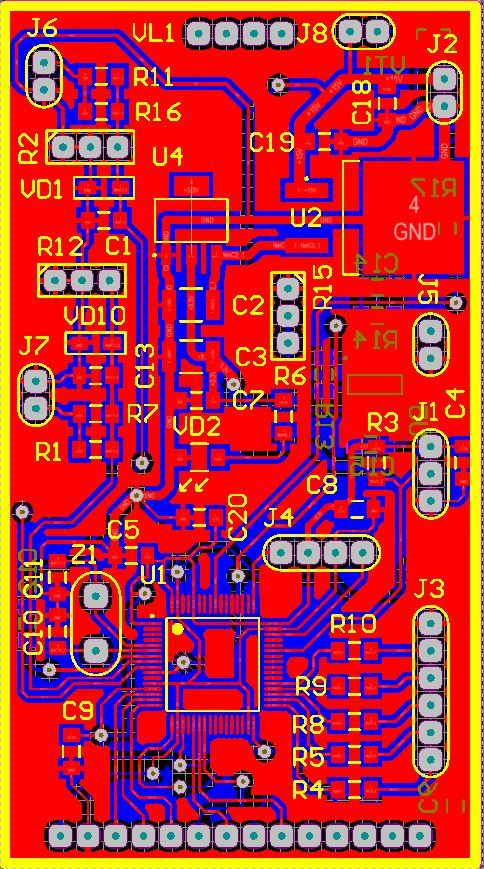
Figure 11 - Board Top Layer
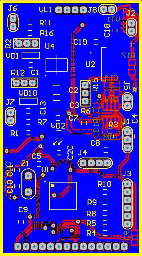
Figure 12 - The bottom layer of the board
PCB file
This is the easiest version of the board, it is for the most newbies, but it works as well as the others and performs its functionality!
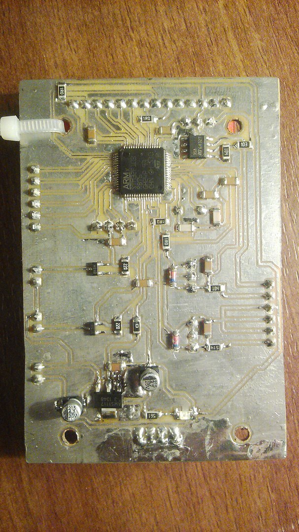
Figure 13 - Board view from the conductors (bottom)
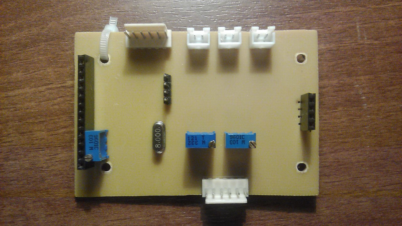
Figure 14 - Top view without TFT, there are hidden quartz, programming connector and trimmer divider resistors
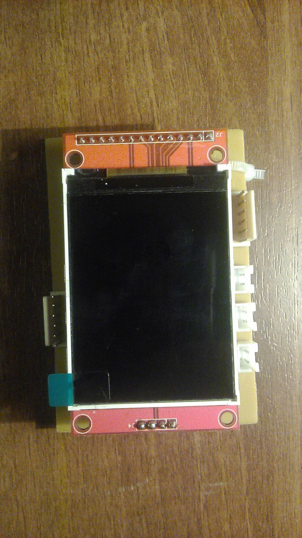
Figure 15 - Top view with a TFT screen, all the "twists" are hidden and you will not knock down the settings at random
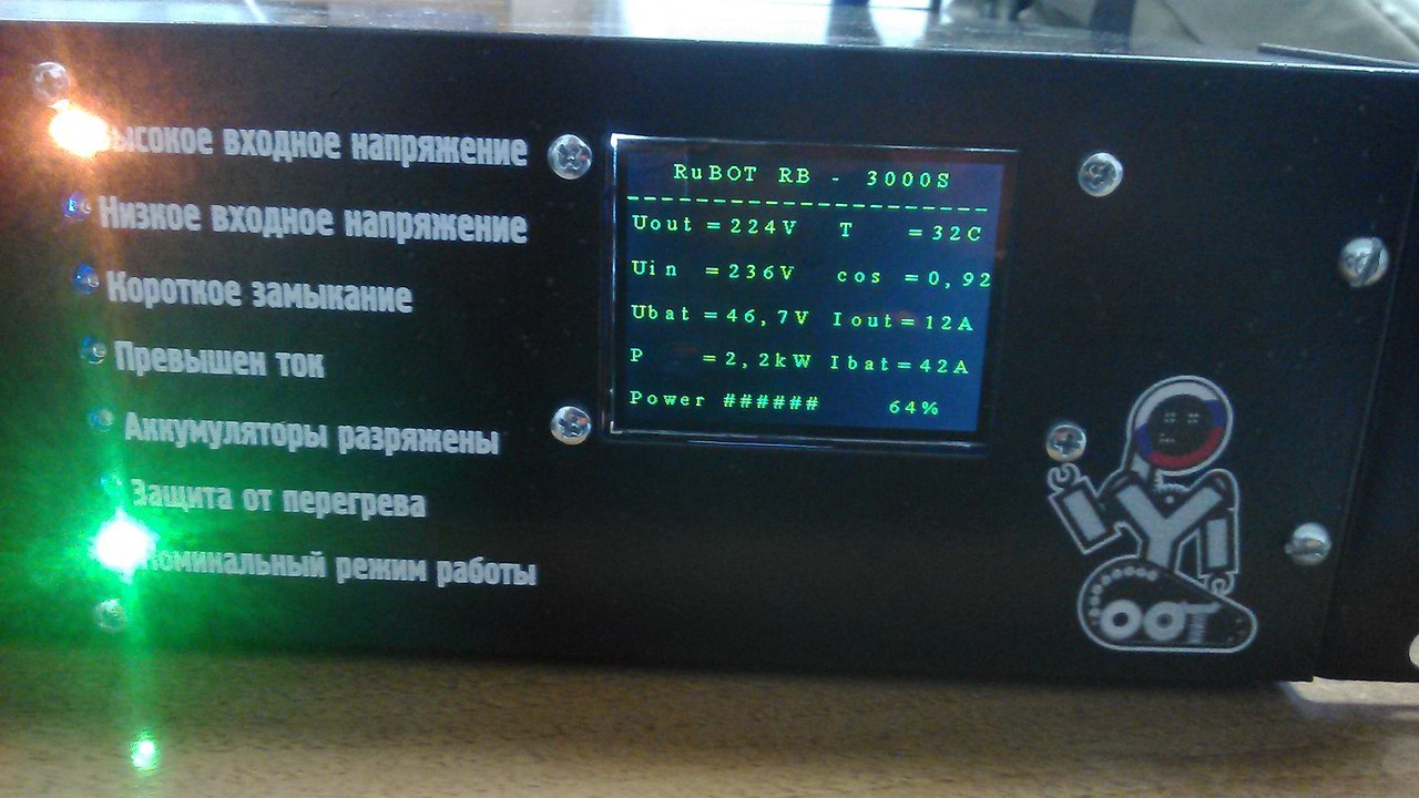
Figure 16 - The whole part of this article was devoted to this very indication.
In principle, this is all that I wanted to tell in this part - namely circuitry and the general principle of operation of the module. And of course the file with the board attached. The code for this device will be a separate part, since This is a very global part of the device and it is better to devote a separate article to it.
Here I would like to know the opinion of readers: is it worth it to parse the code? Does it make sense to lay out the source code and parse them? Perhaps it is enough to attach a ready .hex firmware and that's it? And most importantly - do you need an article on the program part? I can simply attach the source to this article for self-analysis, or chew in a separate part, for example, "Part 4.2"
Thanks to all readers, I look forward to your opinion on the future movement.
Part 4.2
Part 5
Part 6
Part 2
Part 3
Prologue
Good day to all and this is the last part of the cycle dedicated to the non- power part of the device. Perhaps you will think that I deliberately tighten the power modules, but this is not so. I just would like to finish with all the side modules that are partly "decorative", but without which our UPS turns into a pile of poorly working iron with an incomprehensible purpose.
Therefore, this article will discuss in detail the implementation of the measurement of voltages, currents in the nodes, as well as temperature control and protection from overheating. And of course - an indication of where we are without it! Indeed, without it, it is quite problematic to understand what is going on with our device, how well it works and whether it works at all.
A few more statements before the start:
1) In the industrial version, the board was divorced in 4 layers for the implementation of high-quality trace of the board, with galvanic isolation and minimal noise, but in this article I will give two types of trace and both for "radio amateurs"! One view is a double-sided board, the other option is one-sided. I can immediately note that even these options have more than enough noise properties for reliable operation, and the galvanic isolation has been removed to reduce the cost of manufacturing, because This node is not responsible and in the event of a malfunction, the device will continue to operate and signal an incident that has occurred.
Of course, before putting them into the article, I made a prototype, hard I drove it and appreciated more than suitable survivability. I also checked the possibility of making these boards with the help of LUT and photoresist - a step of 0.3 mm is achieved without problems.
')
2) Anyone who wants to repeat this unit or the entire UPS, I am ready to send the programmed STM32 microcontroller if its presence scares you away. The price will be: the cost of MK + shipping, solely for the purpose of helping, and not making money.
Some clarity seemed to have introduced, then we went to understand the scheme ...
General circuitry and description of module functions
And so the general scheme of the module that will be discussed today, rewritten it specifically for this article on modules, so that newbies find it easier to understand the general principle of operation and what “piece” is responsible for what in the final functional:
Figure 1 - Schematic diagram of the display and control unit on the STM32F103RBT6
Now we are looking at the scheme and can roughly imagine that it can:
1) the first thing is striking "rectangle" with the inscription ILI9341. This is a color TFT screen with a resolution of 240x320 pixels and a diagonal of 2.4 ". Almost all the information about the measurements will be displayed on it.
2) we also see an inscription near one of the “Shunt” connectors, which I think suggests measuring the current with good accuracy. This is exactly what justifies the use of a current shunt in this circuit, and not a current transformer. The latter are used in power modules for protection against short circuits (short-circuit)
3) we also see a pair of connectors labeled "+ 360V" and "+ 48V" - this is monitoring the voltage on the DC bus (including the battery) and measuring the output voltage. Simply, to reduce the time constant of the circuit, it was decided to carry out measurements in a high-voltage DC circuit, since the output voltage (AC) linearly depends on it, so it is not difficult to recalculate the constant to alternating voltage at the output of the UPS
4) those who worked with the DS18B20 sensor will immediately pay attention to the J1 connector; this is where we will connect our thermal sensor
5) The sensor is a feedback circuit for cooling coolers that connect to connector J8.
6) there is a magic J3 connector, which has a bunch of identical resistors and LED inscriptions around it, probably everyone guessed that the same LED indication was connecting here that you could see on the front panel of the UPS
The general possibilities of the scheme were discussed, you need to make out how each block works.
Functional unit operation principles and program management
1) Let's start with the most important thing - with nutrition, you can't break a diet. If someone suddenly forgot the previous article - the power supply at us has a voltage of 15V, we need to power all our good from this voltage, taking into account that the microcontroller is powered by 3.3V.
Figure 2 - Supply Stabilization Circuits
Stabilizers are all linear, because The current in the + 3.3V circuit will not exceed 0.25A. There is one fundamental point - the presence of seemingly excess LM7805 stabilizer. In fact, I somehow got into such a situation that my stabilizer on AMS1117-3.3 was burning like a fly, and all because I was used to 7805, 7815 and the like - they have a maximum input voltage of up to 40V. AMS1117 has a maximum input voltage of 12V. Therefore, if we give 15V to it, it will burn so that this does not happen we first reduce our 15V to 5V and then 5V to 3.3V.
It seems to be a trifle, but I, because of inattention and habit, somehow in one project got on a dead STM32F407VET stone and a bunch of SDRAM. LED VD2 - just signals the presence of voltage in the power line.
2) Now we need our stabilized power supply to the MC - we will use the available stone STM32F103RBT6. The reasons for his choice will be in the next paragraph. And so the main rule of wiring - a lot of capacitors in the power supply does not happen. At a minimum, there should be 1 0.1 μF capacitor for each pair of legs V cc - V ss . Of course, the power supply circuit of the analog part of V dda should be diluted differently - there should be a separate electrolyte, a choke ... This is all cool, but for consumer tasks and with not very high accuracy, the usual capacitor like in other circuits will suffice.
An ideal variant of the power scheme can be found in the datasheet on any STM.
Figure 3 - Microcontroller power circuit
We still see our V bat - it serves to control the power in the line; if it is lowered, it can lead the MK into sleep mode or economy mode. In our problem, this is not relevant, since It is used in systems with battery power, such as a player or phone.
What are capacitors in the circuit for - in order to filter out noise and spikes on the power supply, to eliminate interference. This is especially true for the power supply circuit of the analog part, because measurement accuracy will depend on it.
3) Here I would like to explain why it is STM32F103RBT6. The F10x series is very similar to each other, the first MK that I tried on the ST was the STM32F100RBT6, which stands on the STM32VL-Discovey debug board. It is almost identical to ours and I ran around working with the display on it, but there is one drawback. Our display on ILI9341 works through hardware SPI , which means its speed depends on the frequency of the MK. The F100 is 24 MHz, quite solid, considering the cost at the ATmega8 level, but at this frequency the SPI was not enough to update the image on the TFT with a frequency invisible to the human eye. Therefore, I decided to take a senior friend and the choice fell on the STM32F103RBT6. As I wrote above, the stones are almost the same, the pinout of their legs is the same, roughly speaking - a complete analog. That's just the clock frequency he has already 72 MHz ! Beyond for any AVR-ki and so necessary to us! At such a frequency, the full screen refresh time with a “bare” SPI is 780 ms, which is still noticeable to the eye. Although if you do not update the entire screen, but the inscriptions on it, then nothing is noticeable already. Of course, we don’t need more, but because the project will be open, then maybe someone decides to add the function of
Figure 4 - General view of the STM32F103RBT6 microcontroller in the LQFP-64 package
4) Since our device is a power device and there is something to warm it, it is necessary to implement the temperature control function. It is made on the legendary DS18B20 sensor, which works on the 1-Wire interface “chewed” on the Internet and books. What is he good at? It fulfills our two requirements: it can measure with an accuracy of + -0.5 and is easy to use. In industrial performance, the same sensor is worth it, it's just 3 of them, but this is redundant for the average man, although no one will forbid you to also use 3 of them for each radiator.
Figure 5 - Connecting a DS18B20 sensor to a microcontroller via a 1-Wire interface
As you can see - everything is so crazy! No difficulties, beyond the wiring requirements of the board and so on. From the diagram it follows that our sensor is connected through the connector, since he himself is attached to the radiators - the main source of heat. The sensor itself is in the TO-92 package. How to work with it programmatically, we will analyze further.
5) The STM32 programming interface is the simplest Serial-Wire interface, which is already made of 3 wires: ground + clock frequency (CLK) + data (DIO).
Figure 6 - Microcontroller Programming Interface
I added + 3.3V output to prevent programming the main power supply, but to use the power from the STM32VL-Discovery debug board. I think everything is clear here, just in case I’ll attach a debug photo:
Figure 7 - General view of the STM32VL-Discovery debug board with STM32F100RBT6 stone and ST-link v1.0 programmer on board
If you plan to continue to study my projects and schemes, and there will be a lot of them from welders to HF transceivers , then I strongly advise you to buy a debugging board for you, you can use any fee - according to your budget. If you want cool projects and in-depth research, buy STM32F429-Disco . This fee will cover 95% of your needs, although the price is about 2.5 - 3 thousand rubles.
6) Measurement of operating voltages is implemented on two ADC channels, this STM has 16 such channels, so there are still more possibilities. We are also interested in 2 values : low-voltage DC bus 48V and high-voltage DC bus with 360-400V. Circuitry is the simplest: voltage divider on resistors, one of which is trimmer and voltage adjustment is performed by changing the coefficient. division .
Figure 8 - ADC input circuits for voltage measurement
The formula for calculating the division ratio:
The formula for the dependence of the voltage on the ADC on the input voltage (measured):
The ADC at STM can measure voltages from 0 to + 3.3V, our task is to choose the coefficient. division so that after the voltage divider 400V and 48V fall into this range. It is desirable that the nominal measured voltage falls approximately at the level of 2V on the ADC, that is, slightly more than the middle. This will measure both smaller and more voltages.
Shunt capacitor - will save us from the pulsations and wrong counting of the ADC, and the Zener diode will protect the input of the ADC MK from overvoltage and ripple, if any.
7) Current measurement is implemented using standard shunts with a nominal drop of 75 mV at 150A . Such a low voltage ADC can measure, but the accuracy and sampling will be low . To solve this problem it is necessary to use an operational amplifier (op amp). It will strengthen us our 75 mV 20 times and we get 1.5V at rated load. Reserve "top" is selected to control the starting and overload currents. After all, we have a stated characteristic of a 200% overload for 20 minutes, and this will create a voltage of 3V on the ADC.
Figure 9 - Implementation of the current measurement circuit at the LM358 op amp
The gain is adjusted by a divider on R13 and R15, by changing it (by adjusting R15 ) we can adjust the current reading. The scheme of inclusion of the OS in general is standard. The only critical moment that arose in my mind is unstable work from + 3.3V. I understand something about this, but in the documentation it was somehow superficially mentioned, I advise you to read the datasheet. Therefore, it was decided to power the DU from + 15V, which we have from duty sources.
8) The last module is the management of the cooling system. It is made on 2 coolers, feedback for their control is performed on the above-mentioned DS18B20. Load control is carried out by power field worker IRLML0030. It is good because it can safely switch the current to 3-4A, and the letter “L” in the markings means that it can work from a low logic level, that is, from + 3.3V. This allows us to directly manage the key from the MC. Controlled rotational speed of coolers using PWM . It is in STM32 hardware, with 4 channels for each timer, and there are many timers ... so there is room for creativity)
I put both coolers on one channel, because it is simply simpler and in this case there is no point in implementing multi-channel control . Feedback "duty cycle - temperature" allows you to maintain the temperature normal to work, as well as to increase (save) the life of the coolers.
Figure 10 - Scheme of the power circuit control cooler using PWM
Resistor R17 is selected within 100 - 1000 ohms, even though the field-effect transistor opens with voltage and ideally does not consume current, but still its gate has a capacitance. She, in turn, will strive to charge an infinitely large current for an infinitely small time, this is of course all in the ideal model. In reality, the gate capacitance will be charged with a sufficiently large current, and therefore it must be limited so as not to kill the MC. Conclusion STM can give about 10-15 mA or 50-80 mA to the entire port, but the stone is not power, and therefore should not be overloaded. Therefore, we follow the simplest path - we put a current-limiting resistor.
I described its rating above, it is better not to set less than 100 Ohms - the resistor will warm up and the current consumed from the MC will be large. It is not advisable to set more than 1 kΩ. the current will be severely limited, the shutter will charge for a long time and the shape of the PWM will be distorted, and this is not very good. I hope this moment I have explained in some detail.
Boards for display module
Option of manufacturing a two-sided board for LUT:
Figure 11 - Board Top Layer
Figure 12 - The bottom layer of the board
PCB file
General view of the board in one-sided execution
This is the easiest version of the board, it is for the most newbies, but it works as well as the others and performs its functionality!
Figure 13 - Board view from the conductors (bottom)
Figure 14 - Top view without TFT, there are hidden quartz, programming connector and trimmer divider resistors
Figure 15 - Top view with a TFT screen, all the "twists" are hidden and you will not knock down the settings at random
Figure 16 - The whole part of this article was devoted to this very indication.
Epilogue
In principle, this is all that I wanted to tell in this part - namely circuitry and the general principle of operation of the module. And of course the file with the board attached. The code for this device will be a separate part, since This is a very global part of the device and it is better to devote a separate article to it.
Here I would like to know the opinion of readers: is it worth it to parse the code? Does it make sense to lay out the source code and parse them? Perhaps it is enough to attach a ready .hex firmware and that's it? And most importantly - do you need an article on the program part? I can simply attach the source to this article for self-analysis, or chew in a separate part, for example, "Part 4.2"
Thanks to all readers, I look forward to your opinion on the future movement.
Part 4.2
Part 5
Part 6
Source: https://habr.com/ru/post/358322/
All Articles