Designing low-power DC-DC for the organization of emergency power. Part 3
Part 1
Part 2
With the previous two articles, I managed to interest a large number of readers - and this is a reason to continue the cycle of articles and try even more. Many of you urgently require circuitry, so what - it's time! It will be a fairly simple article, it will be a bunch of standard solutions and a fewtricks with the ears of clever circuit solutions.
True, if you have not forgotten - my task is not just to produce a result formonkey mindless repetition , but to explain why every detail and explain how it all works. Therefore, nothing miraculous in this article, you definitely will not see the difference.
It's no secret that there is such a thing as galvanic isolation. This is a circuit technique with which we electrically isolate different parts of our circuit. Most often in practice it is necessaryto isolate in a similar way to untie the high-voltage input part (where we have the mains voltage) and the low-voltage part (output, where we have +15 V).
All this is necessary so that during the operation of the power supply unit (DC-DC converters) of the user, it simplydoesn’t stumble and kill the high voltage that may be output at any fault. It is possible that any power transistor “breaks through” in the circuit, it organizes short circuits, that is, it will pass current from the input directly to the output. In the circuit where there is no electrical isolation at the output instead of + 15V will be + 310V, I think the difference is clear to everyone.
')
I hope at this stage you understand the general essence of the galvanic isolation, and that you should not neglect it, although it often at times complicates the circuit. Moving on ...
1) Applying a transformer. If we remember the principle of operation of a transformer, we will understand that its primary and secondary windings are in no way electrically connected, and energy is transmitted through a magnetic field. That is why you will not kill charging from the phone. In power devices, primary (high-voltage) and secondary (low-voltage) are decoupled exclusively by means of a transformer! Remember this and live a little longer.
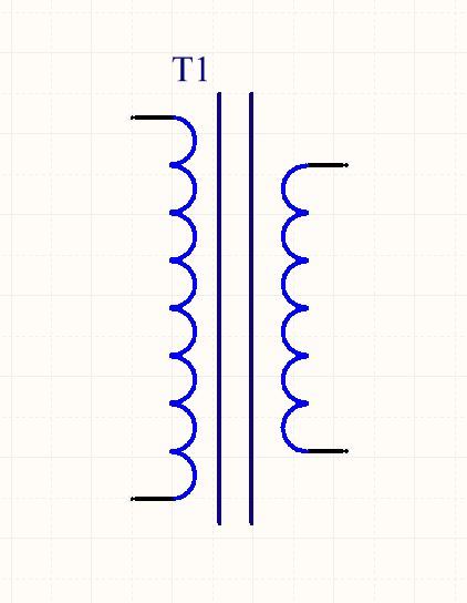
Figure 1 - Transformer as a node of electrical isolation
2) I use optocouplers. This method implements optical isolation, it is used in control circuits. The optocoupler is simply installed - inside it there is a LED and a phototransistor. They are unrelated, except for the light flux. When we light the LED of the optocoupler, it lights the phototransistor and it already passes the current. The end here is obvious! The light does not transmit electricity, so the two halves of the optocoupler are not connected electrically.
Such afeint with ears circuitry technique allows us in the event of a power unit failure to prevent high voltage from getting to the control chips, and they are expensive. A maximum of optocouplers burn, or rather a phototransistor in it. We will have to replace only one part in management instead of a whole board with dozens of elements.

Figure 2 - Optocoupler RS817 as a means of decoupling the control circuit
Let's return to the task ... Comparing the text above with our idea about the UPS, I think you have already guessed that we will need a galvanic isolation in all power units. What we need to do:
1) Untie the UPS input from the DC bus on which the batteries sit, imagine what they will say if instead of 56 V they get 310 V - obviously not thanks;
2) Unleash the DC bus from the device output, we do not need direct current there, and 230 V breaks on the battery especially;
3) Electrically isolate all control modules ( brains ) from high-voltage circuits for their integrity in the event of an accident, as well as reducing the level of interference from power elements.
From the theses above it is necessary to draw the following conclusion: it is necessary to realize a separate power supply to the control elements and power units.
To solve this problem, we need 2 "+15 V" lines: one will power the control boards, the other power switches. Immediately I will clarify why we need +15 V in power modules - the field effect transistor, like the IGBT, opens with voltage. The typical voltage required to open the key is just 12-18V, we will choose the “middle ground”. We realize it simply - we wind 2 secondary windings that will work independently of each other. You can stabilize only one way out, because the windings are identical and the voltage on them with equal duty ratio will be equal.

Figure 3 - Using two isolated windings on one transformer
We also need to remember that if we make a stand-by power supply unit, which, from the input 230V AC, will do on 15V DC, we will not solve the whole problem, since in the event of a voltage drop in the input network, we will be left without our 15 V and all our control elements will go out together with the UPS. I think such a device and UPS will be difficult to name.
This problem can be solved in several ways, but I will go along the most difficult (relatively) way - an additional power supply unit (DC-DC), which will allow us to convert our 48V DC to the required 15V DC. The task seems to have cleared everything up:
a) AC-DC converter 220 - 15 V, power 60 V, which will allow us to easily remove the current 4A, which will be more than enough in this case to open transistors;
b) DC-DC converter 48 - 15 V, the same power of 60 watts.
I use the experience of past years, I immediately decided on what I would do this IIP. The choice fell on an excellent family of chips - TOP22x . This microcircuit contains a high-voltage switch, a driver, a short-circuit current protection, is able to start from high voltage and has the “soft start” skill. All this reduces the external strapping scheme well, just to a minimum! And the price for this miracle is only $ 1-2 at retail, wholesale is cheaper.
For this money, we get almost ready to use SMPS with a capacity of up to 150 W, in the 22x series - the last digit is directly related to the maximum power. TOP227 used by me is capable of 100-120 W, I have never squeezed the declared 150 W or my hands are not from there.

Figure 4 - Schematic diagram of the SMPS with a capacity of 60 W and an output voltage of 15 V
Go through the scheme:
1) Anticipating the question "where ishis mother your KKM or PFC?", I will answer right away - I have a PFC common to the whole device and powering this 230V SMPS comes after it, so you can not install it. If you use this power supply in other constructions, then an input filter is still needed, at least a ferrite ring on the supply wire;
2) Classic rectifier: diode bridge and electrolytic capacitor - cheap and cheerful. The only feature in front of the diode bridge is a capacitor labeled "X1" , that Google will tell it in detail, and I just say that it works perfectly in the fight against interference and pulses, and X1 is the type. So I advise him to put in all the IIP at the entrance. After this node we get - 310 V DC. For all the impulse technology works with direct current.

Figure 5 - Pulse Power Supply Rectifier Assembly (SMPS)
3) The transformer has 4 windings on its board: 1 primary + 2 secondary + 1 self-powered. The self-powered winding is not electrically isolated, since is not an output, so the "earth" of the high-voltage part and this winding are combined.
4) Node with TOP227 microcircuit. Here, special attention should be paid to wiring on the C8-R1 circuit board: these two elements should be located as close as possible to the leg C (control).

Figure 6 - TOP227 chip feedback circuit
5) In parallel to the primary winding, we see two cunning diodes: a suppressor and a pulsed diode. Usually at this moment “professionals” fly withevidence of the level of the Ren-TV channel with not a reasoned statement: “It is necessary to install snubber!” Guys, snubber really makes sense in welding inverters to get the necessary form of IVC. In the IIP came the age of suppressors. These 2 tricky diodes will protect our microcircuit from EMF emissions, which can exceed the limit of 700 V for the internal key TOP227. They work simply: the suppressor is the same Zener diode, only faster and more powerful, so it will extinguish all the pulses above 400 V , and a pulsed diode that has a very short breakdown time will help it. I advise you to use a similar bundle in all SMPSs - this will protect your transistors, which are quite expensive.
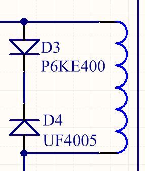
Figure 7 - Protection of the power switch against high voltage emissions at the primary winding of the transformer
6) Rectifiers in this scheme are standard: half-wave rectifier from one diode, electrolyte, choke and a pair of capacitors after. Such a fairly simple rectifier and medium OS make it possible to obtain pulsations not higher than 20-25 mV. A half-wave rectifier is not the most efficient thing, but it took its deserved niche to be simple and at low power.
As we see, we have 3 “lands”: GND - high-voltage side + self-power winding, GND2 and GND3 - two independent lands, such circuitry allowed us to get 2 galvanically isolated windings, both from the network and from each other. One will feed the digital part, the other - the power.

Figure 8 - Half-wave rectifier in the secondary circuits
7) Voltage feedback is quite a “classic” one - it is built on the legendary TL431, a datasheet circuit for it. R10 and R2 - form a voltage divider, by adjusting R2, you can change the coefficient. division and, accordingly, the voltage at the output. R6 and VD5 serve as an indication of the output voltage to visually assess the performance of the unit.
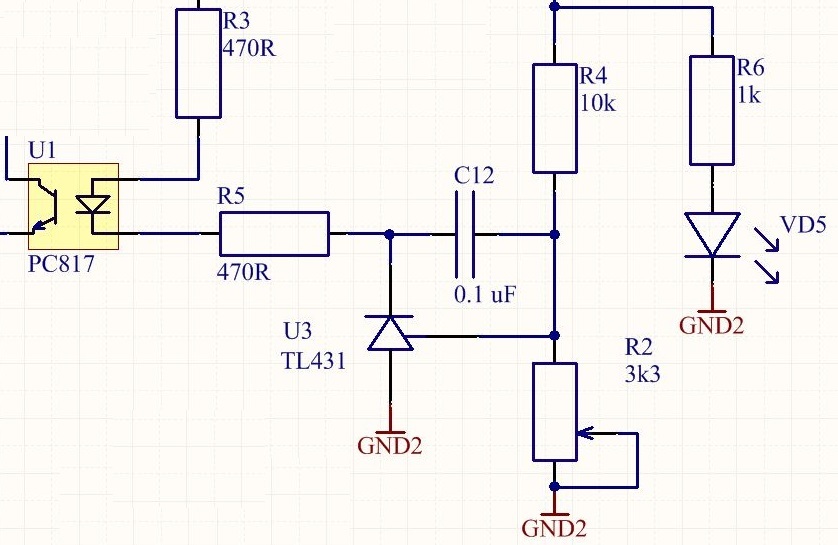
Figure 9 - Voltage feedback based on TL431 and PC817
8) The last thing worth mentioning, and the first in importance, the capacitors C7 and C13 unite the "ground", it is necessary for the stable operation of the OS. They do not bind the "earth" galvanically. I also mention that these are not simple capacitors, but the “Y2” type . Details about them will be in the same place as about X1. This capacitor is able to withstand high-voltage pulsations, as well as equalizes the potentials on the "lands".
The topic of flyback converters or flyback is chewed on the Internet is nowhere more detailed, but I will briefly tell you the general principle of work, because The article is aimed at beginners.
From the name “flyback” - one can guess that he performs some important action (physical process) on the reverse course. And more specifically, our microcircuit generates control pulses - a PWM signal. It has 2 states: 1 and 0. For "1" we have adopted an open transistor, for "0" - a closed one.

Figure 10 - Single-phase converter status diagram
The diagram shows that +310 V to the primary winding is absolutely always supplied. In order for current to flow, it remains to connect the “ground” to the other end of the primary winding. There will be a potential difference and the current will flow. As we see on the wiring diagram, the output transistor TOP227 takes 2 states: open “1” connects the ground to the primary winding, closed “0” disconnects the ground from the primary winding and thereby interrupts the current. All these changes come with a frequency of 100 kHz, that is, very quickly.Your KO
At the moment when the state is “1”, the key is open and current flows in the primary winding — energy is stored, the primary winding, like the usual choke, stores energy in a magnetic field. At this moment there is no current on the secondary windings. When the state changes to “0” and the current in the primary winding stops flowing, then there is a “release” of energy through the core into the secondary winding and there is a current due to self-induced EMF. In general, the primary winding all.
In the secondary we get a pulsating current to get it even we use capacitors and a choke. At the moment of state "0", when the current in the secondary winding is, they accumulate excess energy. When the state "1" and there is no current in the secondary windings, the stored energy from the capacitors and the inductor begins to "release" and create a current - compensating for its absence in the winding.
Fuh ... I hope explained clearly. Please, those who are particularly aware not to throw slippers into some pseudo-bloopers, they are allowed only to develop an understanding of the operation of a pulse transformer!
How to make it and wind it, read in Part 2 of this series of articles. Here I will give only an example of calculation in the Flyback 7.1 program and a few photos from the stage of transformer winding:
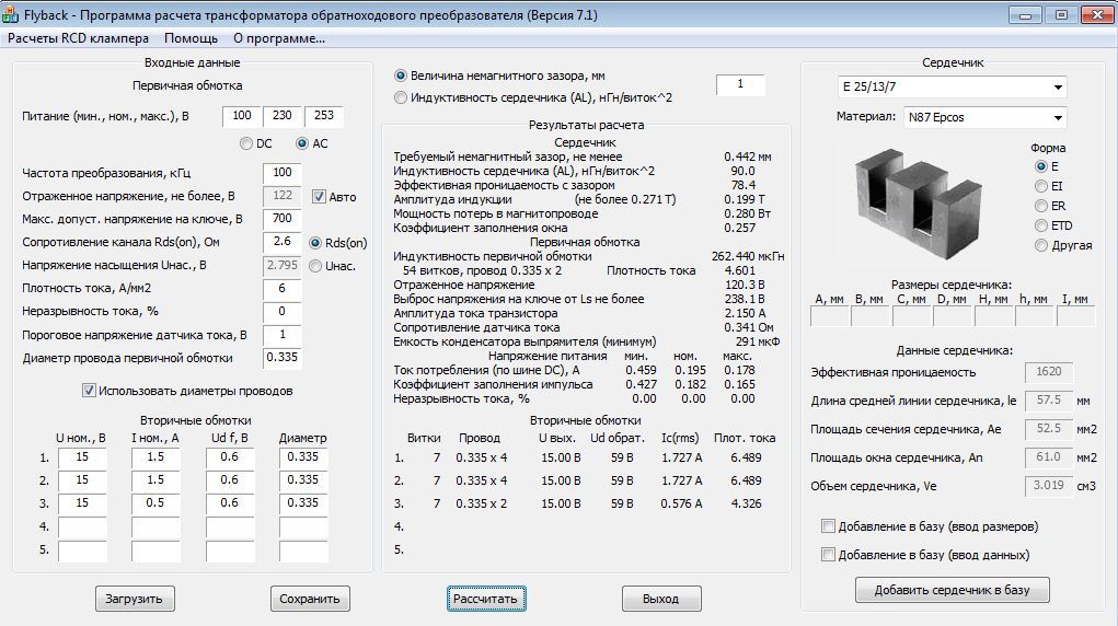
Figure 11 - Calculation of winding parameters for our transformer

Figure 12 - winding the primary winding
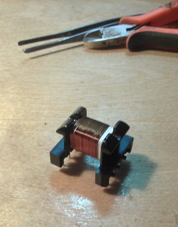
Figure 13 - wound the primary winding

Figure 14 - Winding the power supply winding

Figure 15 - Wound secondary power windings, they are already in several wires
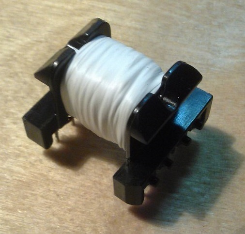
Figure 16 - After winding all layers we isolate, it remains to put on the core and glue it

Figure 17 - Upper layer of the PCB
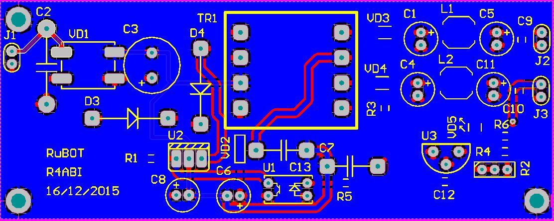
Figure 18 - The bottom layer of the PCB

Figure 19 - Displaying the board model to identify silk-screening jambs
Now the view of the first prototype, it is homemade (made by photoresist + Wood alloy), was made in one-sided version and with one secondary power winding. It is on these layouts all driven around. Of course, a photo of the sample with factory boards and other things will be in a separate photo session! For now:

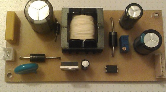
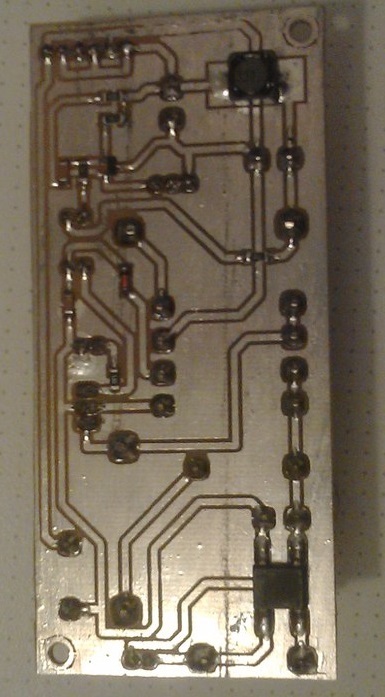
Figure 20-22 - Board of the first working prototype on which it was possible to obtain the required current in 4A and 18 mV ripple
Given that my article has grown quite strongly, but I will describe this block briefly, because as intended, it is identical to the first in TOP227. We will consider the detailed work of this topology in the part about 48 -> 400 V, dedicated to power DC-DC inverter. In the meantime, I offer materials:
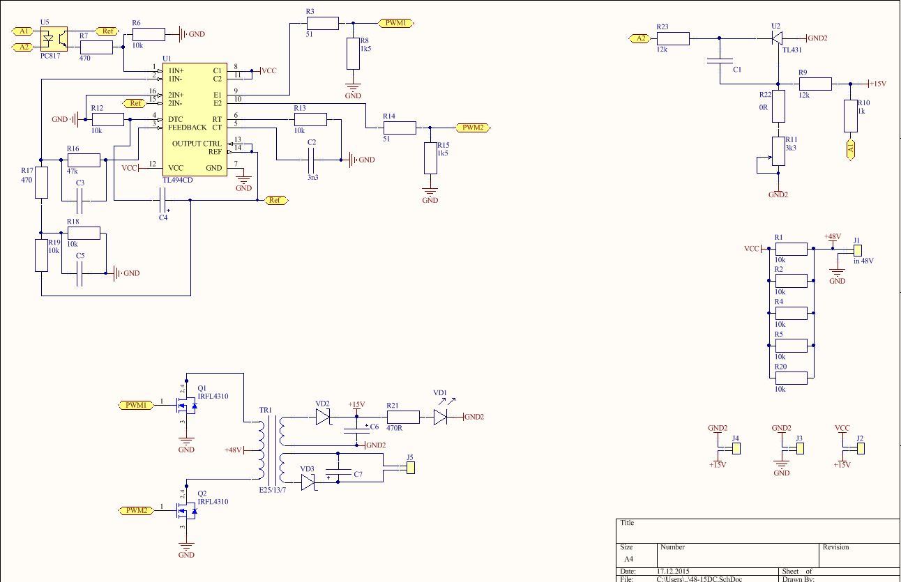
Figure 23 - Schematic diagram of the DC-DC converter on the push-pull topology

Figure 24 - Transformer calculation table for the converter. Current 1A is selected because in the event of a shutdown, this module will have to power only half of the device
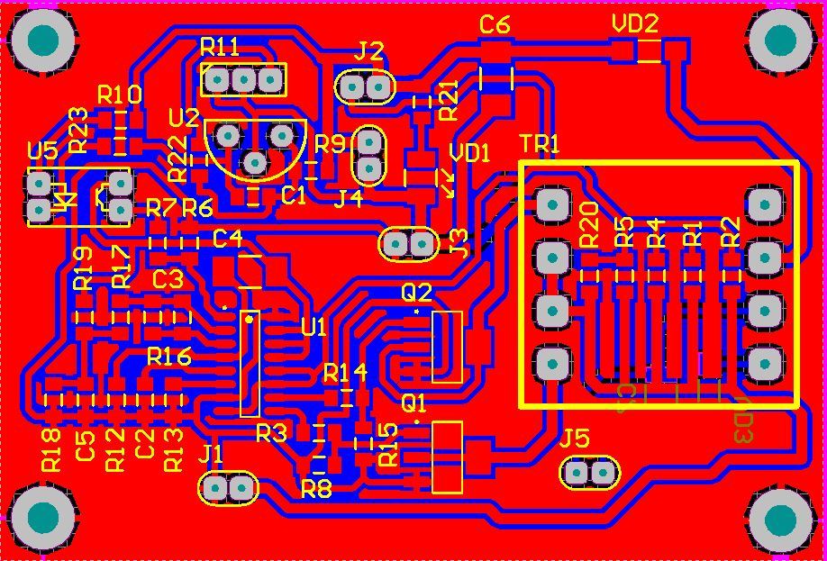
Figure 25 - Board Top Layer

Figure 26 - The bottom layer of the board
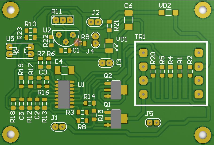
Figure 27 - Model of the printed circuit board for assessing the correctness of screen printing
That ended essentially the first article on the circuitry of the UPS. I hope the material did not disappoint you, any wish and criticism is always happy to listen. Since The next article will be more global, then it will be released on the weekend, most likely on Saturday. Those who wish to begin the repetition of the design will be happy to help with advice and materials.
Just as you probably noticed - the documentation in the folder I did not provide, this is a subtle hint that everyone has not mastered the urgent development of Altium, comrades!
Thanks to everyone who reads and actively discusses my articles! To be continued as always ...
After listening to the criticism and advice from the readers decided to add a second option for distributing flyback.

Figure 28 - Bottom side of the board
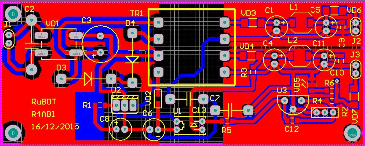
Figure 29 - Top side of the board

Figure 30 - Fee without polygon filling
Part 4.1
Part 4.2
Part 5
Part 6
Part 2
Prologue
With the previous two articles, I managed to interest a large number of readers - and this is a reason to continue the cycle of articles and try even more. Many of you urgently require circuitry, so what - it's time! It will be a fairly simple article, it will be a bunch of standard solutions and a few
True, if you have not forgotten - my task is not just to produce a result for
The task that needs to be solved
It's no secret that there is such a thing as galvanic isolation. This is a circuit technique with which we electrically isolate different parts of our circuit. Most often in practice it is necessary
All this is necessary so that during the operation of the power supply unit (DC-DC converters) of the user, it simply
')
Remember! All subsequent circuits will be high voltage! You should work very carefully if you decide to repeat.
I hope at this stage you understand the general essence of the galvanic isolation, and that you should not neglect it, although it often at times complicates the circuit. Moving on ...
How can you realize galvanic isolation:
1) Applying a transformer. If we remember the principle of operation of a transformer, we will understand that its primary and secondary windings are in no way electrically connected, and energy is transmitted through a magnetic field. That is why you will not kill charging from the phone. In power devices, primary (high-voltage) and secondary (low-voltage) are decoupled exclusively by means of a transformer! Remember this and live a little longer.
Figure 1 - Transformer as a node of electrical isolation
2) I use optocouplers. This method implements optical isolation, it is used in control circuits. The optocoupler is simply installed - inside it there is a LED and a phototransistor. They are unrelated, except for the light flux. When we light the LED of the optocoupler, it lights the phototransistor and it already passes the current. The end here is obvious! The light does not transmit electricity, so the two halves of the optocoupler are not connected electrically.
Such a
Figure 2 - Optocoupler RS817 as a means of decoupling the control circuit
Let's return to the task ... Comparing the text above with our idea about the UPS, I think you have already guessed that we will need a galvanic isolation in all power units. What we need to do:
1) Untie the UPS input from the DC bus on which the batteries sit, imagine what they will say if instead of 56 V they get 310 V - obviously not thanks;
2) Unleash the DC bus from the device output, we do not need direct current there, and 230 V breaks on the battery especially;
3) Electrically isolate all control modules ( brains ) from high-voltage circuits for their integrity in the event of an accident, as well as reducing the level of interference from power elements.
From the theses above it is necessary to draw the following conclusion: it is necessary to realize a separate power supply to the control elements and power units.
To solve this problem, we need 2 "+15 V" lines: one will power the control boards, the other power switches. Immediately I will clarify why we need +15 V in power modules - the field effect transistor, like the IGBT, opens with voltage. The typical voltage required to open the key is just 12-18V, we will choose the “middle ground”. We realize it simply - we wind 2 secondary windings that will work independently of each other. You can stabilize only one way out, because the windings are identical and the voltage on them with equal duty ratio will be equal.
Figure 3 - Using two isolated windings on one transformer
We also need to remember that if we make a stand-by power supply unit, which, from the input 230V AC, will do on 15V DC, we will not solve the whole problem, since in the event of a voltage drop in the input network, we will be left without our 15 V and all our control elements will go out together with the UPS. I think such a device and UPS will be difficult to name.
This problem can be solved in several ways, but I will go along the most difficult (relatively) way - an additional power supply unit (DC-DC), which will allow us to convert our 48V DC to the required 15V DC. The task seems to have cleared everything up:
a) AC-DC converter 220 - 15 V, power 60 V, which will allow us to easily remove the current 4A, which will be more than enough in this case to open transistors;
b) DC-DC converter 48 - 15 V, the same power of 60 watts.
Back-down DC-DC Converter
I use the experience of past years, I immediately decided on what I would do this IIP. The choice fell on an excellent family of chips - TOP22x . This microcircuit contains a high-voltage switch, a driver, a short-circuit current protection, is able to start from high voltage and has the “soft start” skill. All this reduces the external strapping scheme well, just to a minimum! And the price for this miracle is only $ 1-2 at retail, wholesale is cheaper.
For this money, we get almost ready to use SMPS with a capacity of up to 150 W, in the 22x series - the last digit is directly related to the maximum power. TOP227 used by me is capable of 100-120 W, I have never squeezed the declared 150 W or my hands are not from there.
Now the very scheme of the low-power SMPS:
Figure 4 - Schematic diagram of the SMPS with a capacity of 60 W and an output voltage of 15 V
Go through the scheme:
1) Anticipating the question "where is
2) Classic rectifier: diode bridge and electrolytic capacitor - cheap and cheerful. The only feature in front of the diode bridge is a capacitor labeled "X1" , that Google will tell it in detail, and I just say that it works perfectly in the fight against interference and pulses, and X1 is the type. So I advise him to put in all the IIP at the entrance. After this node we get - 310 V DC. For all the impulse technology works with direct current.
Figure 5 - Pulse Power Supply Rectifier Assembly (SMPS)
3) The transformer has 4 windings on its board: 1 primary + 2 secondary + 1 self-powered. The self-powered winding is not electrically isolated, since is not an output, so the "earth" of the high-voltage part and this winding are combined.
4) Node with TOP227 microcircuit. Here, special attention should be paid to wiring on the C8-R1 circuit board: these two elements should be located as close as possible to the leg C (control).
Figure 6 - TOP227 chip feedback circuit
5) In parallel to the primary winding, we see two cunning diodes: a suppressor and a pulsed diode. Usually at this moment “professionals” fly with
Figure 7 - Protection of the power switch against high voltage emissions at the primary winding of the transformer
6) Rectifiers in this scheme are standard: half-wave rectifier from one diode, electrolyte, choke and a pair of capacitors after. Such a fairly simple rectifier and medium OS make it possible to obtain pulsations not higher than 20-25 mV. A half-wave rectifier is not the most efficient thing, but it took its deserved niche to be simple and at low power.
As we see, we have 3 “lands”: GND - high-voltage side + self-power winding, GND2 and GND3 - two independent lands, such circuitry allowed us to get 2 galvanically isolated windings, both from the network and from each other. One will feed the digital part, the other - the power.
Figure 8 - Half-wave rectifier in the secondary circuits
7) Voltage feedback is quite a “classic” one - it is built on the legendary TL431, a datasheet circuit for it. R10 and R2 - form a voltage divider, by adjusting R2, you can change the coefficient. division and, accordingly, the voltage at the output. R6 and VD5 serve as an indication of the output voltage to visually assess the performance of the unit.
Figure 9 - Voltage feedback based on TL431 and PC817
8) The last thing worth mentioning, and the first in importance, the capacitors C7 and C13 unite the "ground", it is necessary for the stable operation of the OS. They do not bind the "earth" galvanically. I also mention that these are not simple capacitors, but the “Y2” type . Details about them will be in the same place as about X1. This capacitor is able to withstand high-voltage pulsations, as well as equalizes the potentials on the "lands".
How it all works
The topic of flyback converters or flyback is chewed on the Internet is nowhere more detailed, but I will briefly tell you the general principle of work, because The article is aimed at beginners.
From the name “flyback” - one can guess that he performs some important action (physical process) on the reverse course. And more specifically, our microcircuit generates control pulses - a PWM signal. It has 2 states: 1 and 0. For "1" we have adopted an open transistor, for "0" - a closed one.
I will give a certain parody of the state diagram:
Figure 10 - Single-phase converter status diagram
The diagram shows that +310 V to the primary winding is absolutely always supplied. In order for current to flow, it remains to connect the “ground” to the other end of the primary winding. There will be a potential difference and the current will flow. As we see on the wiring diagram, the output transistor TOP227 takes 2 states: open “1” connects the ground to the primary winding, closed “0” disconnects the ground from the primary winding and thereby interrupts the current. All these changes come with a frequency of 100 kHz, that is, very quickly.
At the moment when the state is “1”, the key is open and current flows in the primary winding — energy is stored, the primary winding, like the usual choke, stores energy in a magnetic field. At this moment there is no current on the secondary windings. When the state changes to “0” and the current in the primary winding stops flowing, then there is a “release” of energy through the core into the secondary winding and there is a current due to self-induced EMF. In general, the primary winding all.
In the secondary we get a pulsating current to get it even we use capacitors and a choke. At the moment of state "0", when the current in the secondary winding is, they accumulate excess energy. When the state "1" and there is no current in the secondary windings, the stored energy from the capacitors and the inductor begins to "release" and create a current - compensating for its absence in the winding.
Fuh ... I hope explained clearly. Please, those who are particularly aware not to throw slippers into some pseudo-bloopers, they are allowed only to develop an understanding of the operation of a pulse transformer!
And now actually to him ...
How to make it and wind it, read in Part 2 of this series of articles. Here I will give only an example of calculation in the Flyback 7.1 program and a few photos from the stage of transformer winding:
Figure 11 - Calculation of winding parameters for our transformer
Figure 12 - winding the primary winding
Figure 13 - wound the primary winding
Figure 14 - Winding the power supply winding
Figure 15 - Wound secondary power windings, they are already in several wires
Figure 16 - After winding all layers we isolate, it remains to put on the core and glue it
Now to the printed circuit boards:
Figure 17 - Upper layer of the PCB
Figure 18 - The bottom layer of the PCB
Figure 19 - Displaying the board model to identify silk-screening jambs
Now the view of the first prototype, it is homemade (made by photoresist + Wood alloy), was made in one-sided version and with one secondary power winding. It is on these layouts all driven around. Of course, a photo of the sample with factory boards and other things will be in a separate photo session! For now:
Figure 20-22 - Board of the first working prototype on which it was possible to obtain the required current in 4A and 18 mV ripple
Designing DC-DC converter (48-60 V) to 15 V by Push-Pull topology
Given that my article has grown quite strongly, but I will describe this block briefly, because as intended, it is identical to the first in TOP227. We will consider the detailed work of this topology in the part about 48 -> 400 V, dedicated to power DC-DC inverter. In the meantime, I offer materials:
Figure 23 - Schematic diagram of the DC-DC converter on the push-pull topology
Figure 24 - Transformer calculation table for the converter. Current 1A is selected because in the event of a shutdown, this module will have to power only half of the device
Figure 25 - Board Top Layer
Figure 26 - The bottom layer of the board
Figure 27 - Model of the printed circuit board for assessing the correctness of screen printing
Epilogue
That ended essentially the first article on the circuitry of the UPS. I hope the material did not disappoint you, any wish and criticism is always happy to listen. Since The next article will be more global, then it will be released on the weekend, most likely on Saturday. Those who wish to begin the repetition of the design will be happy to help with advice and materials.
Just as you probably noticed - the documentation in the folder I did not provide, this is a subtle hint that everyone has not mastered the urgent development of Altium, comrades!
Thanks to everyone who reads and actively discusses my articles! To be continued as always ...
UPD
After listening to the criticism and advice from the readers decided to add a second option for distributing flyback.
Figure 28 - Bottom side of the board
Figure 29 - Top side of the board
Figure 30 - Fee without polygon filling
Part 4.1
Part 4.2
Part 5
Part 6
Source: https://habr.com/ru/post/358320/
All Articles