DC / AC inverter: principle of operation, circuitry, firmware
Pulse converters and power electronics in general have always remained something sacred for the majority of amateurs and professionals in the field of electronics development. The article highlights perhaps the most interesting topic among DIY-makers and fans of alternative energy - the formation of a sinusoidal voltage / current from DC.
I think many of you probably saw the advertisement, or read the article, where was the phrase "pure sine." That's it about him and will be discussed, but not about the marketing component, but about only technical implementation. I will try to explain as clearly as possible about the principles of operation, about standard (and not so) circuit solutions, and most importantly, we will write and analyze the software for the STM32 microcontroller, which will generate the necessary signals for us.
Why STM32? Yes, because now it is the most popular MK in the CIS: there is a lot of Russian-language information on them, there are a lot of examples, and most importantly, these MK and debugging tools are very cheap for them. Frankly, in a commercial project, I would put only TMS320F28035 or a similar DSP from the Piccolo series from TI, but this is a completely different story.
')
One thing is important - STM32 allows you to stably control simple “household” power converters on which thefate of the world does not work any NPP or data center.
This is the picture of control signals that must be obtained in order to convert a constant current into an alternating current. And yes - here it is the sine! Like in that movie: “See the gopher? - Not. - And he is ... "
It is interesting to know how the sine is formed? I would like to know how the kilowatts of energy are still pumpingoil ? Then welcome under the cat!
If you ask the crowd of electronics engineers: “How can a sine wave be formed?”, Then sentences with a dozen different methods will sprinkle, but which one do we need? Let's push off from the original task - we need to turn, for example, 380V 10A into alternating voltage 230V. In general, this is a “classic” case, we can see it in any good on-line UPS or inverter. It turns out we need to convert the power to about 4 kW, and even with good efficiency, not weak, right? I think a similar condition will reduce the number of options for "drawing" the sine. So what remains for us?
In power converters up to 6-10 kW, two main topologies are used: a full bridge and a “half bridge” with a through neutral. They look like this :
1) Topology with pass-through neutral
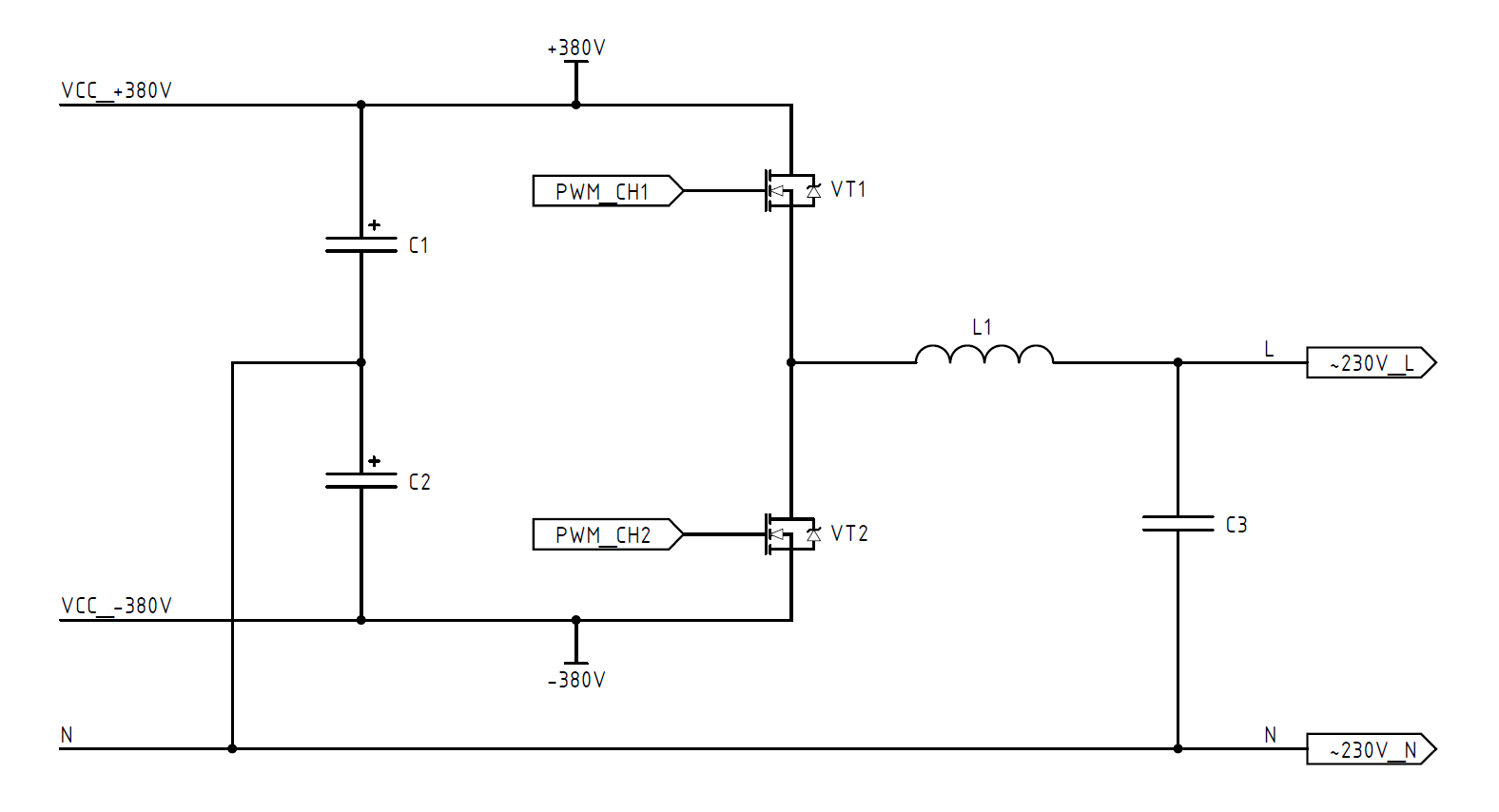
This topology is very often found in budget UPSs with a sine output, although such authorities as APC and GE do not disdain to use it even at sufficiently large capacities. What motivates them to this? Let's look at the advantages and disadvantages of this topology.
The main advantages and disadvantages are determined, so when is this topology necessary? My subjective opinion: at capacities up to 500-1000 W, when cost, not reliability, is a fundamental requirement. An obvious representative of such consumer goods is the stabilizers from “A-electronics”: cheap, it works somehow and well. For 60% of consumers in our country, this is sufficient and affordable. Draw conclusions.
2) Bridge topology
Bridge topology ... probably the most understandable and most common topology in power converters, and most importantly accessible to developers, even with little experience. After 10 kW you will not encounter anything other than a single or three phase bridge. Why is he so loved?
As you can see from the real drawbacks of the bridge topology, there is only an increased requirement for the cooling of transistors. Many will think: "Heat is allocated more - it means efficiency is lower!". Not exactly ... Due to the reduced emissions of EMF and a more “rigid” control system, the efficiency of the two topologies is approximately equal.
In 70% of cases, I have to apply a bridge circuit not only in DC / AC inverters, but also in other converters. This is due to the fact that I design mainly industrial solutions and more often for European customers, and there it has been decided to give a guarantee for 5-15 years for expensive industrial devices. The classical requirement: “We want a piece of iron so that we can give a guarantee of 10 years,” there is no need to choose. Of course, when people want a device with a minimum price, then it is necessary to start from a specific task when choosing a topology.
Small result : this article will provide software for the operation of a bridge converter (H-bridge or Full Bridge), but the principle of sine formation is the same for all topologies. The code can also be adapted for the 1st topology, but this is yourself.
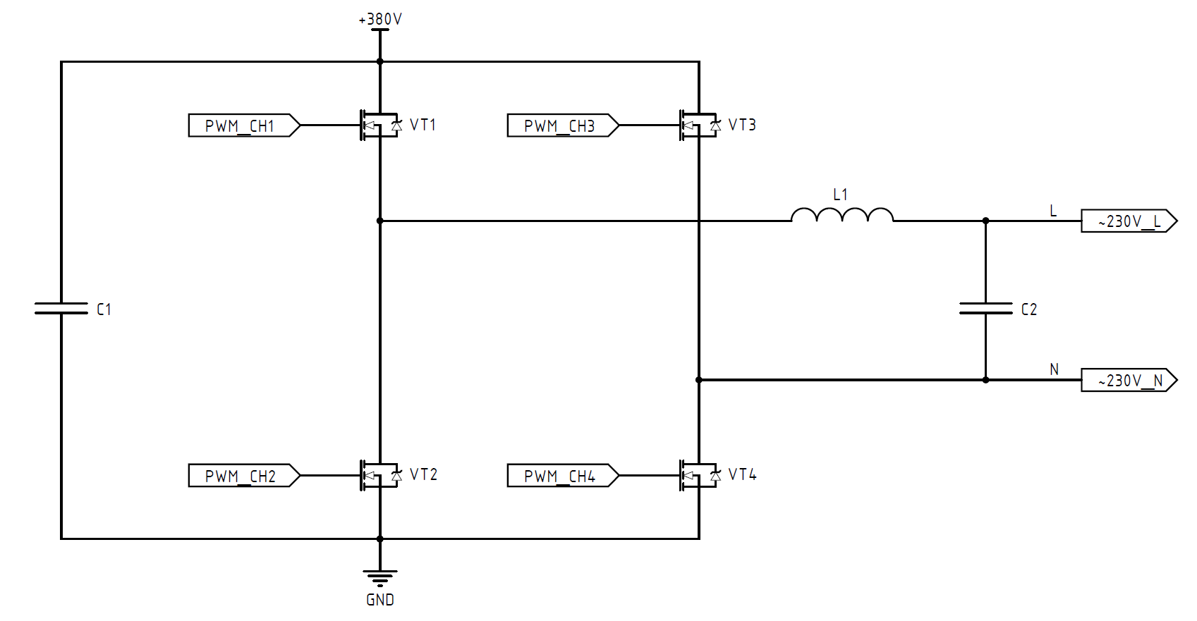
First, let's look at how a bridge converter works. We look at the circuit and see the transistors VT1-VT4. They allow us to apply this or that potential to our abstract load (resistor, for example). If we open the transistors VT1 and VT4, we get the following: VT4 connects one end of the load to minus (GND), and transistor VT1 connects to + 380V, the potential difference “380V - 0V” appears on the load, which is not zero, and therefore the load will begin to flow. I think everyone remembers that scientists have agreed - the current flows “from plus to minus.” We get this picture:
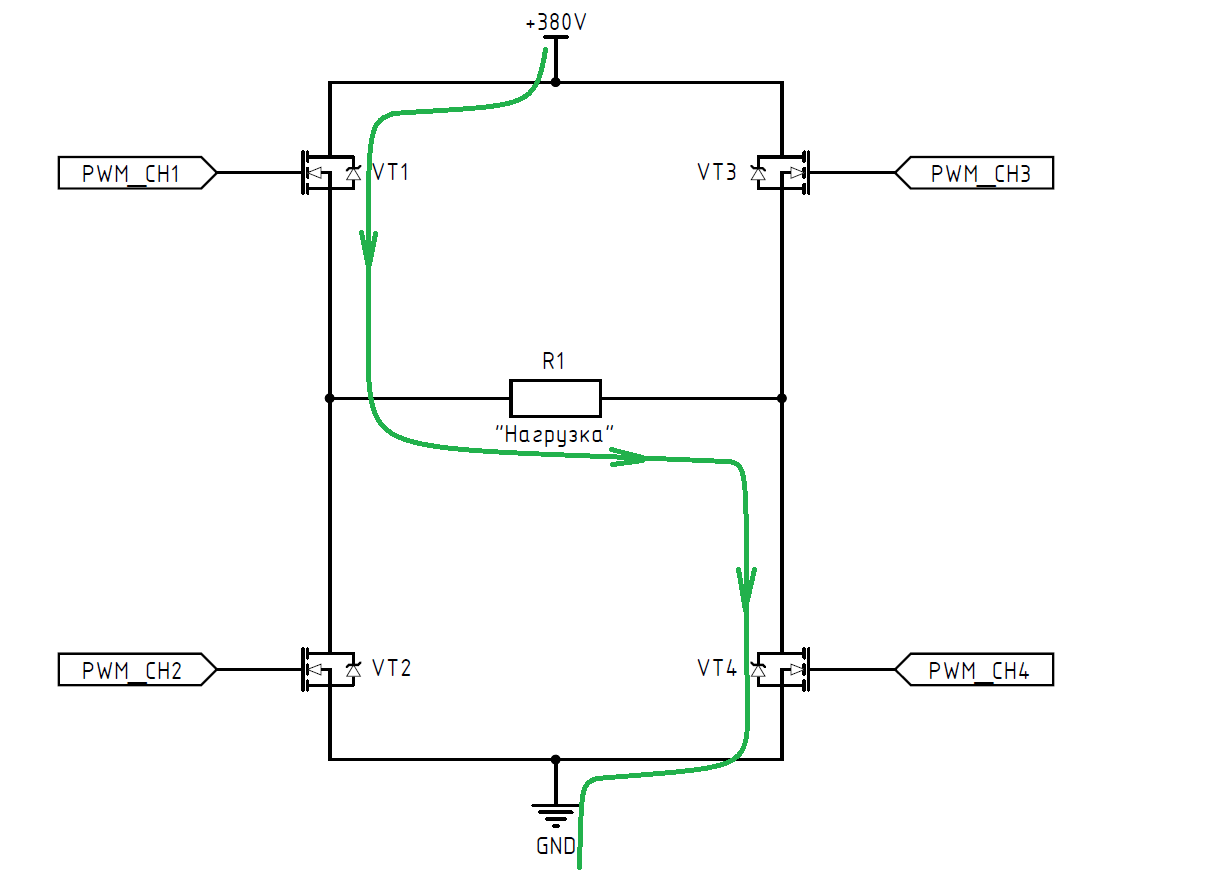
What did we get by opening VT1 and VT4? We connected our load to the network! If the resistor is replaced with a light bulb, then it would just catch fire. And we did not just include the load, but determined the direction of the current flowing through it. It is very important! And what happened at that time with VT2 and VT3? They were closed ... completely ... tightly ... What would happen if all the same VT2 or VT3 were also open? We look:

Suppose that transistors VT1, VT4 and VT2 are opened. We recall Ohm's law, look at the channel resistance of high-voltage transistors, for example, IPP60R099P7XKSA1 and see 0.1 Ohm, we have 2 of them in series - it means the resistance of the circuit VT1 and VT2 is about 0.2 Ohm. Now we calculate the current that goes through this circuit: 380V / 0.2 Ohm = 1900A. I think everyone understands that this is a short circuit? I also think everyone understands why VT2 and VT3 should be closed?
This "phenomenon" is called - through current . And it is with him that there is a big war in power electronics. How to avoid it? Create a control system whose algorithm will strictly forbid the simultaneous opening of an extra transistor.
Why, then, need transistors VT2 and VT3? Remember I wrote that the direction of the current is very important? Let's remember what alternating current is. Actually it is a current that has something variable, in this case the direction of the current. We have a current flowing in the outlet, which changes its direction 100 times per second. Let's now close VT1 and VT4, and then open the transistors VT2 and VT3 and get the following picture:
As you can see the direction of the current (indicated by arrows) has changed to the opposite. Using a bridge allowed us to change the direction of the current, what does that mean? Yes, we got alternating current!
Please note that the bridge has, as it were, 2 diagonals: the first diagonal is formed by VT1 + VT4, and the second diagonal is formed by using VT2 + VT3. These diagonals work in turn, switching the current first in one direction and then in the other.
So we got an alternating current, tell you, but not everything is so simple ... We have a standard - the mains voltage. It is normalized by two main parameters: voltage and frequency. Let's take a look at the frequency for now, because the voltage issue is simple and purely circuitry.
And so the frequency ... that it is known about it - it is 50 Hz (sometimes 60 Hz in the States). The signal period is 20 ms. A sinusoid piece is symmetrical in this case, which means that our 2 half-waves (positive and negative) have the same duration, that is, 10 ms + 10 ms. I hope everything is clear.
What does this mean in the physical sense? Yes, the fact that we need to change the direction of the current in the load every 10 ms. We get that at first we have a 10 ms VT1 + VT4 diagonal open, and then it closes and the VT2 + VT3 diagonal opens for the next 10 ms.
And so, in order for our bridge to change the direction of the current every 10 ms, we need to send a PWM signal to it, the period of which is 20 ms and the duty cycle 50%. This means that in 20 ms the shoulder is half the time (10 ms) open and carries current, and the other half is closed. We need to supply such a PWM to all keys, but with one condition - on the VT1 + VT4 diagonal we submit direct PWM, and on the VT2 + VT3 diagonal already inverse. Speaking more intelligently, the signal supplied to the diagonal should have a 180 o shift. I think at this moment your head is boiling in trying to understand the text, so we are looking at its visual presentation:
Now everything is clear? Not? Then more ... As you can see, I specifically noted the moments of the opening and closing of the transistors: they open at the "plus" and close at the "minus". Also, the signals are opposite, that is, inverse: when the blue signal is “plus”, then the green signal is “minus”. We give a blue signal on one diagonal to one, and a green signal on another - as seen on the oscillogram, our diagonals never open at the same time. AC is ready!
Look at the period. Specially showed the waveform from the controller outputs, so that my words were not an abstraction. The signal period is 20 ms, one diagonal is open 10 ms and creates a positive half-wave, the other diagonal also opens for 10 ms and creates a negative half-wave already. Now I hope everyone understands, and who still do not understand - write in the LAN, I will hold for you an individual lesson on your fingers. In confirmation of my words, the oscillogram shows our cherished 50 Hz! Just relax early ...
We received an alternating current with a frequency of 50 Hz, but we have a sinusode in the socket, and here the meander is not the case. Formally, you can apply the meander to the output and supply them with most of the loads, for example, to a pulsed power supply unit anyway: a sine or a meander. That is, turning on laptops, telephones, televisions, telephones and other things is enough for you, but if you plug in an AC motor, everything will be very bad - it will start to warm up and its efficiency will be significantly less, and in the end it will most likely burn. Do you think you don't have engines at home? And the refrigerator compressor? And a circular heating pump? The latter generally burn as if made of wood. The same situation with deep pumps for wells, and indeed a lot with what. It turns out that a sinusoidal signal at the output of an inverter, stabilizer, or UPS is still important. Well, you need to create it! Now the brain explosion will start ...
Frankly speaking, I do not know how to present this section in an accessible language. Suddenly, whoever does not understand, I ask you either to google it additionally, or write in a comment or a LAN — I will try to explain to you personally. The eyes are afraid, and the hands are doing ...
Let's see what a regular sine plot looks like:
We see 2 axes: one axis with a period of pi, pi / 2 and further, the second with an amplitude of -1 to +1. In our problem, the period is measured in seconds and is 20 ms or 10 ms for each half-wave. Everything is simple and clear, but with amplitude more fun - just accept as an axiom that the amplitude is from 0 to 1000. This is the value of the duty cycle that the microcontroller sets, that is, 100 is 10%, 500 - 50%, 900 - 90 % I think the logic is clear. In the next chapter, you will understand why from 0 to 1000, but for now we will reorganize our graph to our values:

This is how thesmoker’s sinus graph looks like, which corresponds to our task. As you can see, I did not identify negative half-time, because here it is implemented not by using a sinusoidal signal, but by changing the direction of the current by switching the bridge diagonals.
On the X axis, we have time, and on the Y axis, the duty cycle of our PWM signal. We need to draw a sine using SHIM. Remember the geometry at school, how did we build the graphics? That's right, by the points! And how many points? Let's build a sine by several points O1 (0,0) + O2 (5,1000) + O3 (10,0) + O4 (15, -1000) + O5 (20, 0) and we get the following sine:
We have built and see that, in principle, this signal is more like a sine than a normal meander, but it is still not a sine for now. Let's increase the number of points. This is by the way called “signal resolution” or, in this case, “PIM discretization”. And how do you know the coordinates of these points? With the extreme, it was just ...
As I said earlier, the sine is quite symmetrical. If we build 1/4 of the period, that is, from 0 to 5 ms, then duplicating this piece further - we can build a sine for an infinitely long time. And so the formula:

And so in order:
Let’s make an example of conveniently the condition that we have 5 points. It turns out we have 1 step = 1 ms, it will allow you to easily build a schedule. The discretization step is considered simple: the period in which we plot the graph (5 ms) is divided by the number of points. Let's bring the formula to the human mind:

We get a sampling step of 1 ms. The formula for calculating the duty cycle will be, for example, in excel and we will get the following table:
Now back to our sine plot and build it again, but for more points and see how it changes:
As you can see, the signal is much more like a sine, even taking into account my skill in drawing, and more precisely in the level of laziness)) I think the result does not require an explanation? According to the results of construction, we derive an axiom:
And so, how many points will we use ... It is clear that the more the better. How to calculate:
With discreteness of PWM decided, 240 points on the floor of the period with a margin is enough to get the waveform at least as good as the network. Now consider the table, also in excel as the easiest option. We get the following schedule:
The source of the table and values can be taken by reference - here .
We got a sine table and what to do with it? It is necessary to transfer these values with a certain discretization step, which is known to us. It all starts with the fact that the timer was initialized - time 0, duty cycle zero. Next, we count the sampling step of 41.66 μs and write the PWM value from table 13 (0.13%) to the timer, count another 41.66 μs and write 26 (0.26%) and so on all 240 values. Why 240? We have 120 steps for 1/4 period, and we need to draw 1/2 period. The duty ratio is the same, only after they have reached 1000, we write it in the reverse sequence and we get a decrease in sine. At the output, we will have the following waveform:
As you can see, we received a bunch of PWM values in a clearly defined period and its duration is: 240 steps x 41.66 (!) Μs = 9998.4 μs = 9.9984 ms ~ 10 ms. We got half the period for a 50Hz network frequency. As you can see, there are two signals again and they are out of phase, just what is needed to control the diagonals of the bridge. But excuse me, where is the sine you ask? The moment of truth has come! Let's now give the signal from the output of the microcontroller to the low-pass filter, I made a simple low-pass filter on the RC circuits with nominal values of 1.5 kΩ and 0.33 μF (they were just at hand) and I got the following result:

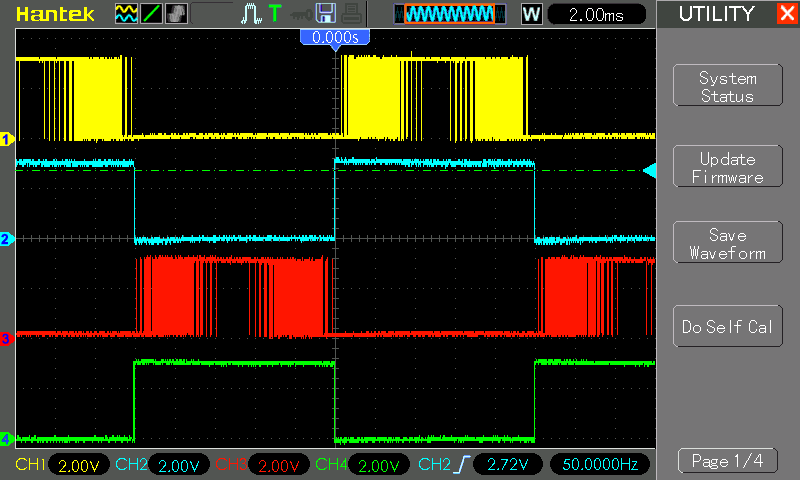
Voila! Here it is our long-awaited sinus! The red beam of the oscilloscope is the signal before the low-pass filter, and the yellow beam is the signal after filtering. LPF cut off all frequencies above 321 Hz. We still have the main signal of 50 Hz, and of course its harmonics with a small amplitude. If you want to clear the signal perfectly, then make a low-pass filter with a cut-off frequency of about 55-60 Hz, but for now it doesn’t matter, we just had to check whether we have a sinus or not. By the way ... I have synchronization of the oscilloscope on the yellow beam (arrow on the right of the screen) and we see its frequency at the bottom of the screen - an ideal 50 Hz. What more could you want? Perhaps everything, it remains to decide what signal and where to submit. Let's look at this picture:

If you draw on the first oscillogram in the article, you will see that the signal in yellow and blue better have the same phase, that is, they become positive at the same time and open the transistors. These 2 signals open VT1 + VT4 diagonal. Accordingly, 2 other signals also have the same phase and open another diagonal. Now we do not just change the direction of the current, but also set the amplitude with the help of PWM so that it varies sinusoidally. Now consider the same schema, but with currents:
As you can see, the current through the load flows in the opposite direction, changing direction with a frequency of 50 Hz, and the modulated PWM applied to the transistors VT1 and VT2 allows you to draw a sinusoidal waveform on half-waves.
Low-pass filter (low-pass filter) is made on inductance L1 and capacitor C2. I advise you to consider the cutoff frequency for this filter to be less than 100 Hz, this will minimize the voltage ripple on the output.
For dessert, I will show part of the scheme of a real device with a similar topology and filter, it is large, so we download the PDF here .
I think it is no secret to anyone that there is nothing perfect? The same with Mosfet-s, they have a number of drawbacks and we will consider one of them - a large gate capacity. That is, in order for us to open the transistor, it is necessary not only to energize, but also to charge the capacitor with this very voltage, therefore the front and falloff of the signal is delayed. This leads to the fact that at the signal boundary there can be a point in time when one transistor has not fully closed yet, and the other has already begun to open.
I advise you to read more about this phenomenon, for example, in this article . I just tell you how to deal with it. So that the transistors have time to close normally before the opening of the next arm between the control signals, they introduce dead-time or, more simply, a time delay. We have such a delay will be introduced between the control signals on transistors VT3 and VT4, because They provide switching half-waves. On transistors with modulated PWM (VT1 and VT2) such delays already exist - the sine begins with a duty cycle of 0% and ends also at 0%. This delay is 1 sampling long, that is, 41.6 μs.
And so - it is necessary to realize the dead time between the blue and the green beam / signal. On any controller, such a delay can be made programmatically, but this is not good - the program will hang or stay and your deviceand apartment will be already on fire. Therefore, in power electronics it is worth using only hardware. On all specialized motor controls, hardware deadtime is provided on all outputs of PWM and channels, but STM32 is still a general-purpose MK, so everything is simpler, but it will perform our function.
We need a timer TIM1, only he knows how to insert a hardware delay between the signals, in the section on writing software, I will tell you how to do it, and now we are looking at the result and what should be in general:
To see the delay, we “stretch” the signal on the oscilloscope, sinceIt has a short duration of about 300 ns. The required time duration of deadtime must be calculated for each specific task in order to protect the transistors from through-currents. The delay time is adjusted when the TIM1 timer is initialized (configured). This delay is present at both the front and the low signal.
So we’ve probably come to the most important and interesting part. We have disassembled the physics of the process, the principle of operation seems to be clear, the necessary minimum of protection is also defined - it remains only to implement all this in real hardware. To do this, I use the STM32VL-Discovery shawl, I got it by the way back in 2011, at a time when ST distributed debugs at their conferences and since then she lay packed - opened the packaging just a couple of months ago, like the shelf life has not passed))) My “stand” for writing the code looks like this:
Now go through the connection. Since I need to form two signals with different frequencies, I had to use the PWM outputs on different timers. TIM1 generates a signal that sets the main frequency of 50 Hz and supplies them to transistors VT3 and VT4. The PIMA channel # 3 + its complementary output is used. Yes, yes, in STM32, hardware deadtime can only be configured between normal and complementary single-channel output, which I didn’t like much. The process of forming the sine itself is transmitted to the timer TIM2, there is no need for a delay here (previously wrote why), and it is quite suitable for generating a modulated signal on VT1 and VT2.
The project is implemented in Keil 5, it will be attached to the archive at the end of the article. I don’t hope to tell how to create a project and similar obvious things, if such questions arise, I advise you to look at how to do it in Google or on youtube. All code is written in CMSIS (registers), because to use any additional levels of abstraction in the converter control system is simply a sin! In ST, these are SPL libraries and more current HALs. For interest I worked with those and with those, the conclusion is full of trash. HAL is so crazy in general, and for applications with hard real-time just doesn’t fit the word at all. In some critical moments, the registers were several times faster, by the way, I found more than one article on the Internet.
Some will surely ask: “Why not use DMA?” This can and should be done, but this article is more of an introductory nature, and the MC itself doesn’t do anything complicated in terms of computation, so the core performance isn’t exactly up to you. DMA is good, but you can do without DMA without any potential problems. Let's clarify what we need to do in the program:
Nothing complicated, right? Then let's go ...
Everything is simple, just an array. The only thing to remember is that we have 120 points from 0 to 1000. We need to add 120 more points to the table, but in reverse order:
Setting clocking in the STM32 is very flexible and convenient, but there are several nuances. The sequence itself looks like this:
1) Switch to clocking from the integrated RC-chain (HSI) to external quartz (HSE), then wait for the ready flag
2) The controller's flash memory is slightly slower than the kernel. For this, we configure flash clocking. If this is not done, the program will start, but will periodically fall: a pair of kW and unstable software are incompatible things.
3) We set up dividers for the system bus clocking (AHB) and for the bus peripherals, of which there are already two pieces: APB1 and APB2. We need the maximum frequency, so we do not divide anything and the division factors are made equal to 1.
4) Adjust the frequency multiplier (PLL) predivider, which stands in front of him and divides the frequency of quartz by 2. We get that 8 MHz divided by 2 and received 4 MHz. Now we need to multiply them by 6, so that the output is 24 MHz. Before writing registers, we first erase their contents just in case.
5) Now you need to turn on the frequency multiplier (PLL) and wait for the readiness flag:
6) Finally, we configure the clock source for the system bus (AHB) output of our frequency multiplier, which has the cherished 24 MHz. Pre-register the contents of the clean, set the desired bit and wait for the ready flag:
As a result, we have this clocking setting function:
I will give a general setting of the timer, it is described in detail in the reference manual - I advise you to read the purpose of each register. And there are basic articles on working with PWM on the Internet. I have very well commented on the code itself, so I’ll quote immediately the code of the function for initializing the timer TIM1, and analyze the most interesting moments:
The duty cycle is fixed and never changes, as well as the frequency. It is this timer that sets the time and sequence of the diagonals:
The duration of the pause "dead time" depends strongly on the TDTS time parameter, which is configured here:
Its duration is 1 clock tick. If you look in the reference manual, you can see that the CKD bits can, for example, make Tdts equal to 2, 8 ticks, and so on.
The very same pause time is set here:
If you open the reference manual RM0041, you will see formulas for calculating DT. As you can see the Tdts parameter is fundamental there:
It’s still easier here, probably there’s no point in explaining something in the setup, for comments are already redundant. If you have questions - wait for them in the comments.
We configure the timer itself at a frequency of 24 kHz:
Major events occur in an interrupt generated by the TIM6 timer. An interrupt is generated every 41.66 μs, if you remember this is our sample rate. Accordingly, in the interrupt, the value of the duty ratio from the table to the CCRx register is written . Also in this interrupt, it is determined which diagonal is currently drawn by inverting the sin_status flag after each half period. We draw 240 points, invert the flag, which causes the control to switch to another channel, when it has already drawn, the flag is inverted again and everything repeats. Main algorithm code:
Download the project, compile and upload to your microcontroller and get a working inverter. All you have to do is make a bridge and give signals to it:

I’ve put some of my bridge schemes in PDF earlier in the PDF, I hope it will help you in mastering power electronics.
Also in the project, I pulled FreeRTOS. Of course, using RTOS means it is impossible to implement similar management tasks, since simple switching between tasks lasts from 4 to 18 microseconds, and that if the code is well written and nothing can hinder the work of the scheduler. This does not allow to get a control system operating in hard real-time. I set up FreeRTOS for another: communication interfaces (RS-485 Modbus RTU), adjustment of the output voltage amplitude, recalculation of the table, synchronization with the 230V network and so on. I will also try to implement all these buns on STM32, and maybe I'll write a continuation of the topic of the article, if interesting results are obtained and there is something to share.
I hope you liked the article. If you have questions on the use of this code in real hardware, I will be glad to answer them. Also, please do not take this code as something ready, this is the core of the converter that implements the main function. All the "buns" and other redundancy you can add yourself. The bare core of the project will allow you to understand how it works and not spend a lot of time disassembling code.
UPD1: I would like to thank the sleip user for a number of errors found, mainly in the sine table - it has been changed. Those who have used the code or the table itself, please copy it again, in the article already corrected version.
I think many of you probably saw the advertisement, or read the article, where was the phrase "pure sine." That's it about him and will be discussed, but not about the marketing component, but about only technical implementation. I will try to explain as clearly as possible about the principles of operation, about standard (and not so) circuit solutions, and most importantly, we will write and analyze the software for the STM32 microcontroller, which will generate the necessary signals for us.
Why STM32? Yes, because now it is the most popular MK in the CIS: there is a lot of Russian-language information on them, there are a lot of examples, and most importantly, these MK and debugging tools are very cheap for them. Frankly, in a commercial project, I would put only TMS320F28035 or a similar DSP from the Piccolo series from TI, but this is a completely different story.
')
One thing is important - STM32 allows you to stably control simple “household” power converters on which the
This is the picture of control signals that must be obtained in order to convert a constant current into an alternating current. And yes - here it is the sine! Like in that movie: “See the gopher? - Not. - And he is ... "
It is interesting to know how the sine is formed? I would like to know how the kilowatts of energy are still pumping
1. Topology for the formation of a sinusoidal signal
If you ask the crowd of electronics engineers: “How can a sine wave be formed?”, Then sentences with a dozen different methods will sprinkle, but which one do we need? Let's push off from the original task - we need to turn, for example, 380V 10A into alternating voltage 230V. In general, this is a “classic” case, we can see it in any good on-line UPS or inverter. It turns out we need to convert the power to about 4 kW, and even with good efficiency, not weak, right? I think a similar condition will reduce the number of options for "drawing" the sine. So what remains for us?
In power converters up to 6-10 kW, two main topologies are used: a full bridge and a “half bridge” with a through neutral. They look like this :
1) Topology with pass-through neutral
This topology is very often found in budget UPSs with a sine output, although such authorities as APC and GE do not disdain to use it even at sufficiently large capacities. What motivates them to this? Let's look at the advantages and disadvantages of this topology.
Pros:
- The minimum possible number of power transistors, which means the loss is 2 times smaller and the cost of the device is also lower
- Pass-through zero. This simplifies the certification process, especially CE and ATEX. This is due to the fact that the through zero allows the input protection systems (for example, RCD) to operate as well when an accident occurs in the output circuits after the converter
- A simple topology that allows us to minimize the cost of the product at small
and medium serial production
Minuses:
- The need for a bipolar power source. As you can see on the inverter circuit should be served ± 380V and zero more
- Doubled the number of high voltage capacitors. High-voltage and high-voltage capacitors with small ESR at capacities from 3-4 kW start to be from 20 to 40%
component cost - The use of electrolytic capacitors in the "divider". They dry, pick up capacitors with the same parameters is almost impossible, and if we consider that the parameters of electrolytes change during operation, it is also meaningless. Replace with a film is possible, but expensive
The main advantages and disadvantages are determined, so when is this topology necessary? My subjective opinion: at capacities up to 500-1000 W, when cost, not reliability, is a fundamental requirement. An obvious representative of such consumer goods is the stabilizers from “A-electronics”: cheap, it works somehow and well. For 60% of consumers in our country, this is sufficient and affordable. Draw conclusions.
2) Bridge topology
Bridge topology ... probably the most understandable and most common topology in power converters, and most importantly accessible to developers, even with little experience. After 10 kW you will not encounter anything other than a single or three phase bridge. Why is he so loved?
Pros:
- Very high reliability. It is mainly due to the quality of the power transistor control system and does not depend on the degradation of components
- Input capacity required at times, and even an order of magnitude less. It is only necessary to provide the estimated value of the ESR. This allows the use of film capacitors while maintaining cost. Film capacitors - do not dry, lead better in harsh temperatures, the working life is much higher than that of electrolytes
- Minimal voltage ripple on transistors, which means that transistors can be applied for lower voltage
- The simplicity and clarity of the algorithms. This leads to a significant reduction in time for product development, as well as for its commissioning.
Minuses:
- The increased number of power transistors, and therefore more serious cooling is needed. The increase in the price of transistors, but at the expense of a smaller number of capacitors, this is more likely even a plus
- Increased driver complexity, especially with requirements for galvanic isolation
As you can see from the real drawbacks of the bridge topology, there is only an increased requirement for the cooling of transistors. Many will think: "Heat is allocated more - it means efficiency is lower!". Not exactly ... Due to the reduced emissions of EMF and a more “rigid” control system, the efficiency of the two topologies is approximately equal.
In 70% of cases, I have to apply a bridge circuit not only in DC / AC inverters, but also in other converters. This is due to the fact that I design mainly industrial solutions and more often for European customers, and there it has been decided to give a guarantee for 5-15 years for expensive industrial devices. The classical requirement: “We want a piece of iron so that we can give a guarantee of 10 years,” there is no need to choose. Of course, when people want a device with a minimum price, then it is necessary to start from a specific task when choosing a topology.
Small result : this article will provide software for the operation of a bridge converter (H-bridge or Full Bridge), but the principle of sine formation is the same for all topologies. The code can also be adapted for the 1st topology, but this is yourself.
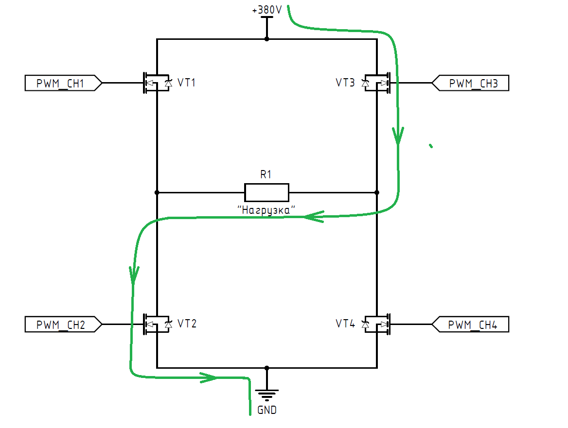
2. Formation of alternating current using a bridge converter
First, let's look at how a bridge converter works. We look at the circuit and see the transistors VT1-VT4. They allow us to apply this or that potential to our abstract load (resistor, for example). If we open the transistors VT1 and VT4, we get the following: VT4 connects one end of the load to minus (GND), and transistor VT1 connects to + 380V, the potential difference “380V - 0V” appears on the load, which is not zero, and therefore the load will begin to flow. I think everyone remembers that scientists have agreed - the current flows “from plus to minus.” We get this picture:
What did we get by opening VT1 and VT4? We connected our load to the network! If the resistor is replaced with a light bulb, then it would just catch fire. And we did not just include the load, but determined the direction of the current flowing through it. It is very important! And what happened at that time with VT2 and VT3? They were closed ... completely ... tightly ... What would happen if all the same VT2 or VT3 were also open? We look:
Suppose that transistors VT1, VT4 and VT2 are opened. We recall Ohm's law, look at the channel resistance of high-voltage transistors, for example, IPP60R099P7XKSA1 and see 0.1 Ohm, we have 2 of them in series - it means the resistance of the circuit VT1 and VT2 is about 0.2 Ohm. Now we calculate the current that goes through this circuit: 380V / 0.2 Ohm = 1900A. I think everyone understands that this is a short circuit? I also think everyone understands why VT2 and VT3 should be closed?
This "phenomenon" is called - through current . And it is with him that there is a big war in power electronics. How to avoid it? Create a control system whose algorithm will strictly forbid the simultaneous opening of an extra transistor.
Why, then, need transistors VT2 and VT3? Remember I wrote that the direction of the current is very important? Let's remember what alternating current is. Actually it is a current that has something variable, in this case the direction of the current. We have a current flowing in the outlet, which changes its direction 100 times per second. Let's now close VT1 and VT4, and then open the transistors VT2 and VT3 and get the following picture:
As you can see the direction of the current (indicated by arrows) has changed to the opposite. Using a bridge allowed us to change the direction of the current, what does that mean? Yes, we got alternating current!
Please note that the bridge has, as it were, 2 diagonals: the first diagonal is formed by VT1 + VT4, and the second diagonal is formed by using VT2 + VT3. These diagonals work in turn, switching the current first in one direction and then in the other.
So we got an alternating current, tell you, but not everything is so simple ... We have a standard - the mains voltage. It is normalized by two main parameters: voltage and frequency. Let's take a look at the frequency for now, because the voltage issue is simple and purely circuitry.
And so the frequency ... that it is known about it - it is 50 Hz (sometimes 60 Hz in the States). The signal period is 20 ms. A sinusoid piece is symmetrical in this case, which means that our 2 half-waves (positive and negative) have the same duration, that is, 10 ms + 10 ms. I hope everything is clear.
What does this mean in the physical sense? Yes, the fact that we need to change the direction of the current in the load every 10 ms. We get that at first we have a 10 ms VT1 + VT4 diagonal open, and then it closes and the VT2 + VT3 diagonal opens for the next 10 ms.
What does it mean to open the transistor and what signal to apply to it
Let's digress a bit on the principle of transistor control. I use Mosfet N-channel field-effect transistors.
An “open transistor” is a transistor whose gate (G) has a positive potential (+ 10..18 V) relative to the source (S) and the transistor has changed the channel resistance (SD) from infinitely large (2-100 MΩ) to small (usually 0.1 - 1 ohm). That is, the transistor began to conduct current.
The “closed transistor” is a transistor whose gate (G) is pulled to the source (S) and its resistance has changed from small to infinitely large. That is, the transistor has ceased to conduct.
For better acquaintance with the principle of operation of a field-effect transistor or IGBT - I advise you to read a couple of chapters in Semenov’s book Fundamentals of Power Electronics, or another source, you can also start Wikipedia.
To control, we give a signal with Pulse Width Modulation or a more familiar abbreviation - PWM. The peculiarity of this signal is that it has 2 states: the lower voltage (GND) and the upper voltage (VCC), that is, by supplying it to the gate of the transistor, we either open it or close it — there is no other way. I also advise you to read about PWM in addition, because I describedto you superficially for the lazy .
An “open transistor” is a transistor whose gate (G) has a positive potential (+ 10..18 V) relative to the source (S) and the transistor has changed the channel resistance (SD) from infinitely large (2-100 MΩ) to small (usually 0.1 - 1 ohm). That is, the transistor began to conduct current.
The “closed transistor” is a transistor whose gate (G) is pulled to the source (S) and its resistance has changed from small to infinitely large. That is, the transistor has ceased to conduct.
For better acquaintance with the principle of operation of a field-effect transistor or IGBT - I advise you to read a couple of chapters in Semenov’s book Fundamentals of Power Electronics, or another source, you can also start Wikipedia.
To control, we give a signal with Pulse Width Modulation or a more familiar abbreviation - PWM. The peculiarity of this signal is that it has 2 states: the lower voltage (GND) and the upper voltage (VCC), that is, by supplying it to the gate of the transistor, we either open it or close it — there is no other way. I also advise you to read about PWM in addition, because I described
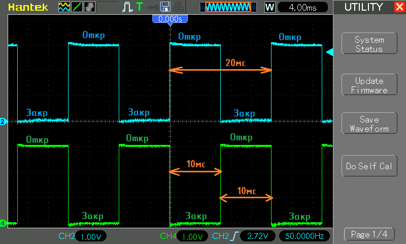
And so, in order for our bridge to change the direction of the current every 10 ms, we need to send a PWM signal to it, the period of which is 20 ms and the duty cycle 50%. This means that in 20 ms the shoulder is half the time (10 ms) open and carries current, and the other half is closed. We need to supply such a PWM to all keys, but with one condition - on the VT1 + VT4 diagonal we submit direct PWM, and on the VT2 + VT3 diagonal already inverse. Speaking more intelligently, the signal supplied to the diagonal should have a 180 o shift. I think at this moment your head is boiling in trying to understand the text, so we are looking at its visual presentation:
Now everything is clear? Not? Then more ... As you can see, I specifically noted the moments of the opening and closing of the transistors: they open at the "plus" and close at the "minus". Also, the signals are opposite, that is, inverse: when the blue signal is “plus”, then the green signal is “minus”. We give a blue signal on one diagonal to one, and a green signal on another - as seen on the oscillogram, our diagonals never open at the same time. AC is ready!
Look at the period. Specially showed the waveform from the controller outputs, so that my words were not an abstraction. The signal period is 20 ms, one diagonal is open 10 ms and creates a positive half-wave, the other diagonal also opens for 10 ms and creates a negative half-wave already. Now I hope everyone understands, and who still do not understand - write in the LAN, I will hold for you an individual lesson on your fingers. In confirmation of my words, the oscillogram shows our cherished 50 Hz! Just relax early ...
We received an alternating current with a frequency of 50 Hz, but we have a sinusode in the socket, and here the meander is not the case. Formally, you can apply the meander to the output and supply them with most of the loads, for example, to a pulsed power supply unit anyway: a sine or a meander. That is, turning on laptops, telephones, televisions, telephones and other things is enough for you, but if you plug in an AC motor, everything will be very bad - it will start to warm up and its efficiency will be significantly less, and in the end it will most likely burn. Do you think you don't have engines at home? And the refrigerator compressor? And a circular heating pump? The latter generally burn as if made of wood. The same situation with deep pumps for wells, and indeed a lot with what. It turns out that a sinusoidal signal at the output of an inverter, stabilizer, or UPS is still important. Well, you need to create it! Now the brain explosion will start ...
3. The formation of a sinusoidal waveform using PWM
Frankly speaking, I do not know how to present this section in an accessible language. Suddenly, whoever does not understand, I ask you either to google it additionally, or write in a comment or a LAN — I will try to explain to you personally. The eyes are afraid, and the hands are doing ...
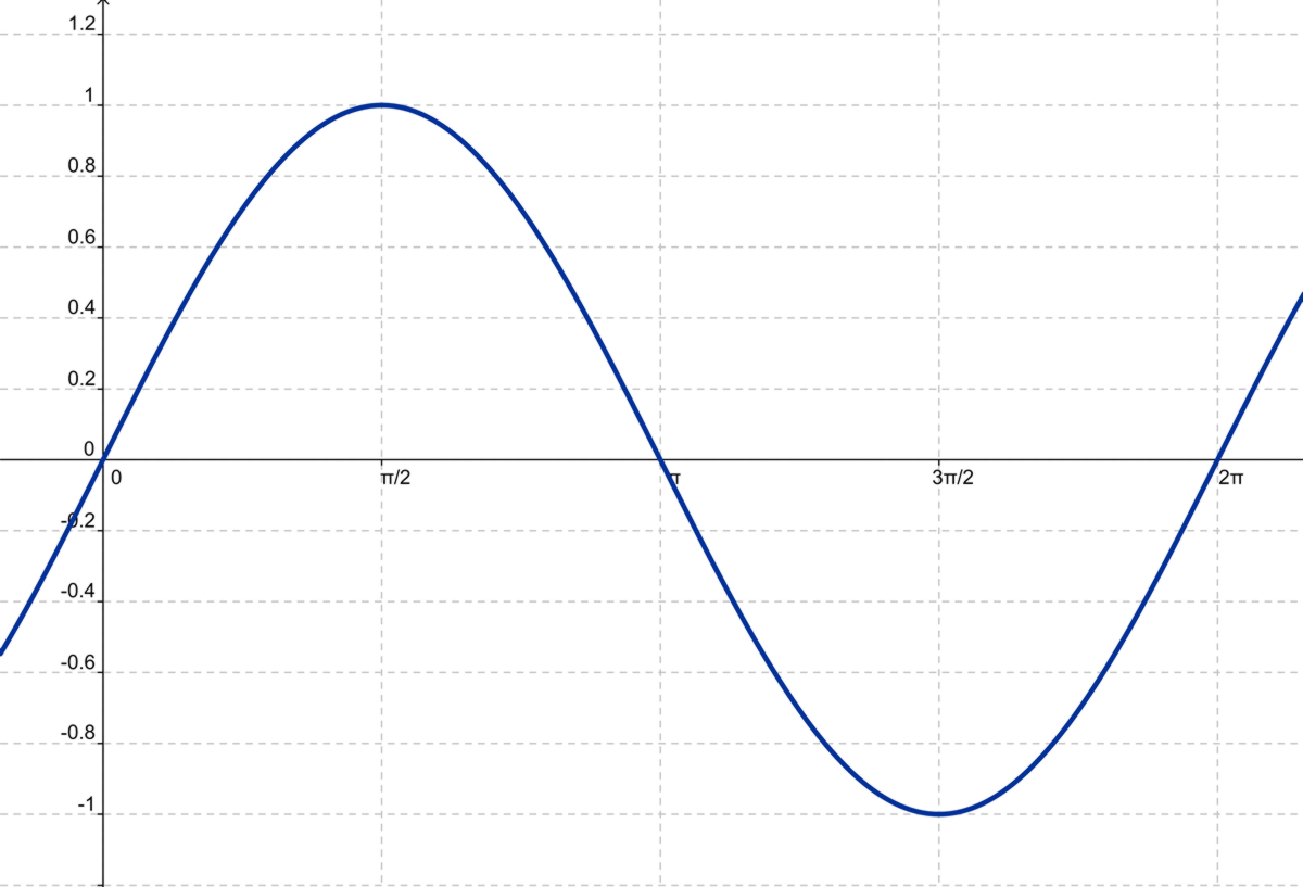
Let's see what a regular sine plot looks like:
We see 2 axes: one axis with a period of pi, pi / 2 and further, the second with an amplitude of -1 to +1. In our problem, the period is measured in seconds and is 20 ms or 10 ms for each half-wave. Everything is simple and clear, but with amplitude more fun - just accept as an axiom that the amplitude is from 0 to 1000. This is the value of the duty cycle that the microcontroller sets, that is, 100 is 10%, 500 - 50%, 900 - 90 % I think the logic is clear. In the next chapter, you will understand why from 0 to 1000, but for now we will reorganize our graph to our values:
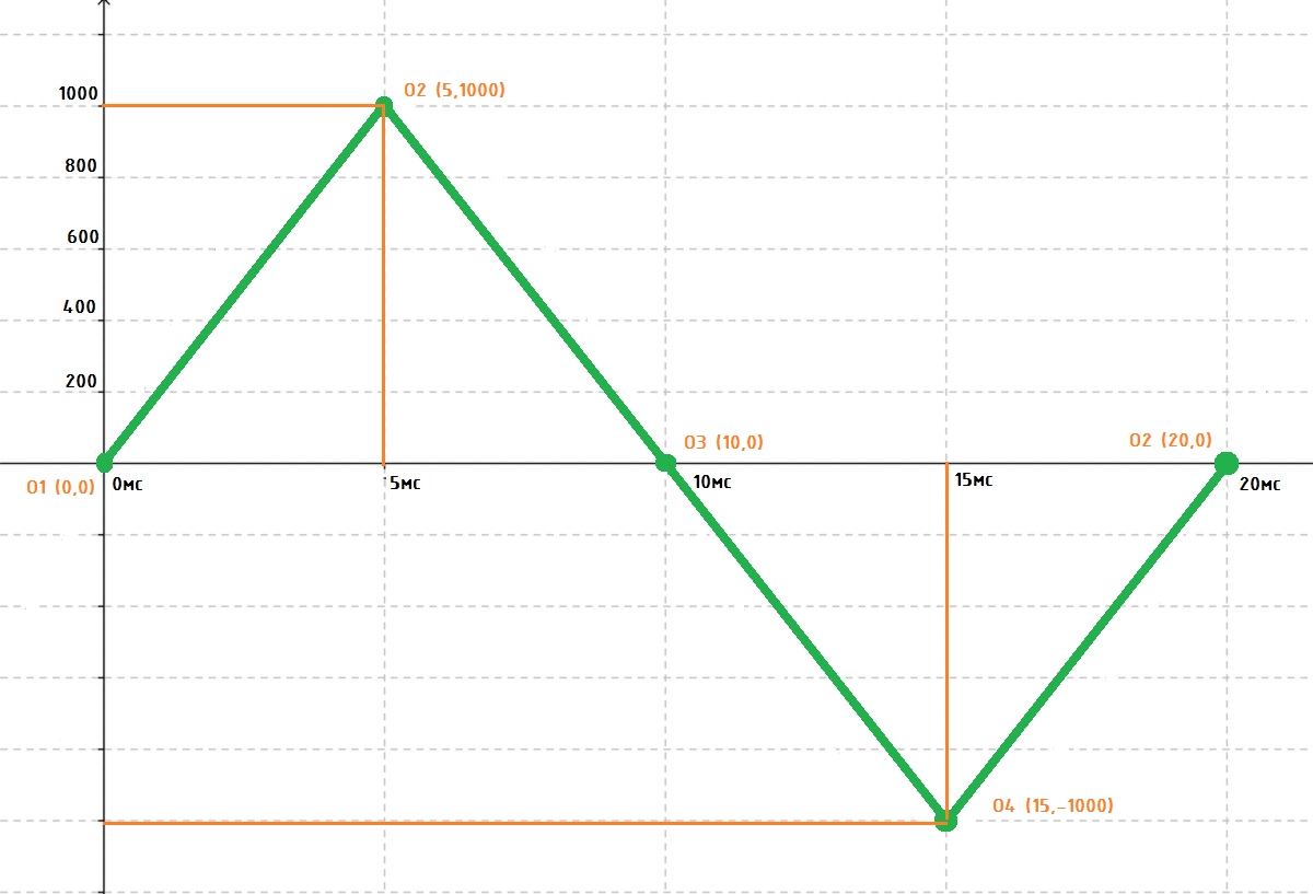
This is how the
On the X axis, we have time, and on the Y axis, the duty cycle of our PWM signal. We need to draw a sine using SHIM. Remember the geometry at school, how did we build the graphics? That's right, by the points! And how many points? Let's build a sine by several points O1 (0,0) + O2 (5,1000) + O3 (10,0) + O4 (15, -1000) + O5 (20, 0) and we get the following sine:
We have built and see that, in principle, this signal is more like a sine than a normal meander, but it is still not a sine for now. Let's increase the number of points. This is by the way called “signal resolution” or, in this case, “PIM discretization”. And how do you know the coordinates of these points? With the extreme, it was just ...
Calculation of values for the formation of sine
As I said earlier, the sine is quite symmetrical. If we build 1/4 of the period, that is, from 0 to 5 ms, then duplicating this piece further - we can build a sine for an infinitely long time. And so the formula:
And so in order:
- n - the value of the duty cycle at this discrete point
- A is the signal amplitude, that is, the maximum value of the duty ratio. We have 1000
- pi / 2 - 1/4 of the sine period falls into pi / 2, if we consider 1/2 of the period, then pi
- x - step number
- N - the number of points
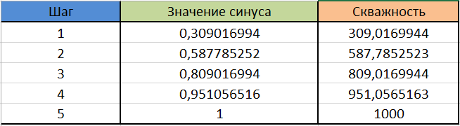
Let’s make an example of conveniently the condition that we have 5 points. It turns out we have 1 step = 1 ms, it will allow you to easily build a schedule. The discretization step is considered simple: the period in which we plot the graph (5 ms) is divided by the number of points. Let's bring the formula to the human mind:
We get a sampling step of 1 ms. The formula for calculating the duty cycle will be, for example, in excel and we will get the following table:
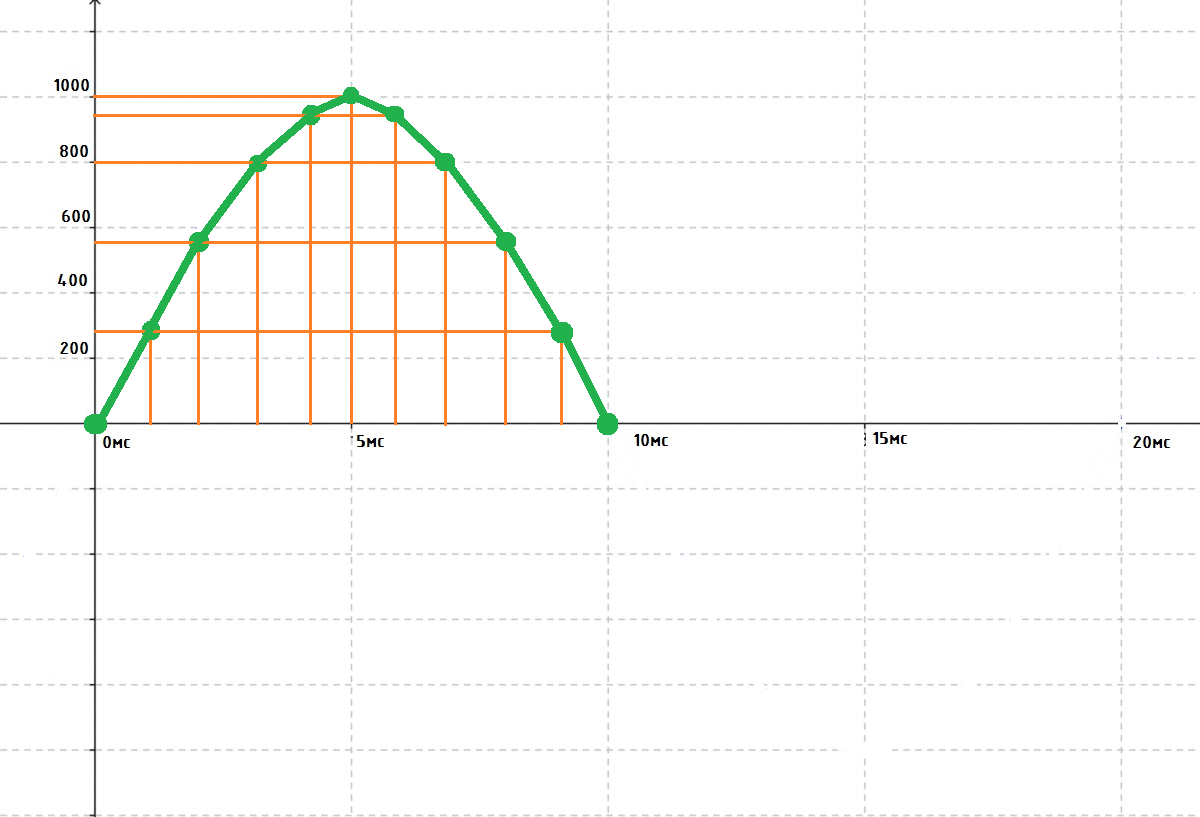
Now back to our sine plot and build it again, but for more points and see how it changes:
As you can see, the signal is much more like a sine, even taking into account my skill in drawing, and more precisely in the level of laziness)) I think the result does not require an explanation? According to the results of construction, we derive an axiom:
The more points, the higher the signal sampling, the more ideal the shape of the sinusoidal signal
And so, how many points will we use ... It is clear that the more the better. How to calculate:
- I use for the article an old microcontroller STM32F100RBT6 (debugging STM32VL-Discovery), its frequency is 24 MHz.
- Consider how many cycles will last a period of 20 ms: 24,000,000 Hz / 50 Hz = 480,000 ticks
- This means half of the period lasts 240,000 ticks, which corresponds to a frequency of 24 kHz. Want to increase the carrier frequency - take the stone faster. 24 kHz, our ears will still be heard, but for tests or a piece of iron, standing in the basement will go. A little later, I plan to transfer to F103C8T6, and there already 72 MHz.
- 240,000 ticks ... It is logical to ask 240 points for half the period. The timer will update the duty ratio every 1000 ticks or every 41.6 μs
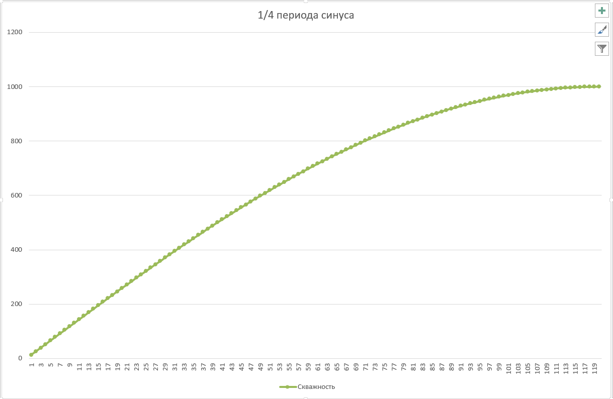
With discreteness of PWM decided, 240 points on the floor of the period with a margin is enough to get the waveform at least as good as the network. Now consider the table, also in excel as the easiest option. We get the following schedule:
The source of the table and values can be taken by reference - here .
4. Control the bridge transducer to form a sine
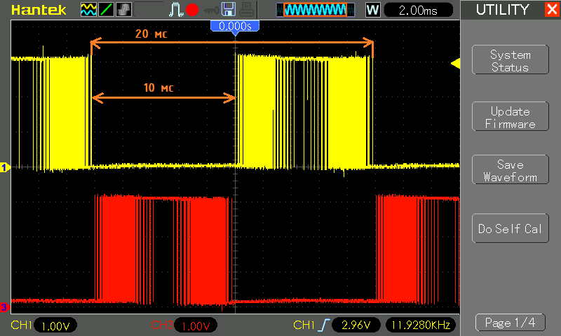
We got a sine table and what to do with it? It is necessary to transfer these values with a certain discretization step, which is known to us. It all starts with the fact that the timer was initialized - time 0, duty cycle zero. Next, we count the sampling step of 41.66 μs and write the PWM value from table 13 (0.13%) to the timer, count another 41.66 μs and write 26 (0.26%) and so on all 240 values. Why 240? We have 120 steps for 1/4 period, and we need to draw 1/2 period. The duty ratio is the same, only after they have reached 1000, we write it in the reverse sequence and we get a decrease in sine. At the output, we will have the following waveform:
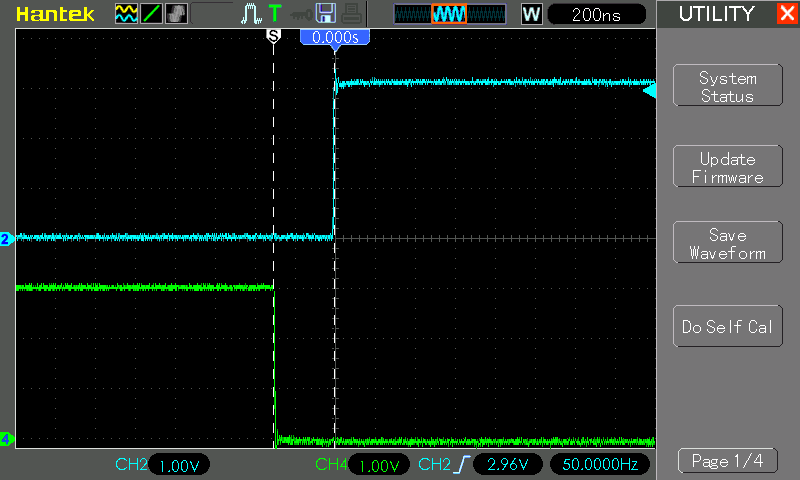
As you can see, we received a bunch of PWM values in a clearly defined period and its duration is: 240 steps x 41.66 (!) Μs = 9998.4 μs = 9.9984 ms ~ 10 ms. We got half the period for a 50Hz network frequency. As you can see, there are two signals again and they are out of phase, just what is needed to control the diagonals of the bridge. But excuse me, where is the sine you ask? The moment of truth has come! Let's now give the signal from the output of the microcontroller to the low-pass filter, I made a simple low-pass filter on the RC circuits with nominal values of 1.5 kΩ and 0.33 μF (they were just at hand) and I got the following result:
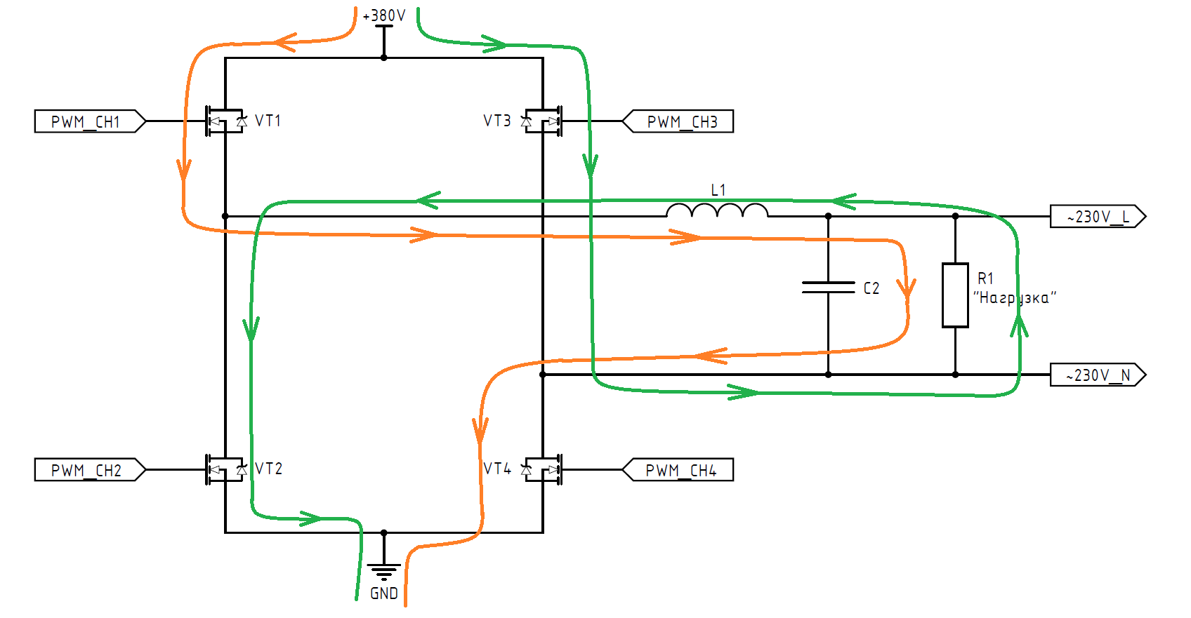
Voila! Here it is our long-awaited sinus! The red beam of the oscilloscope is the signal before the low-pass filter, and the yellow beam is the signal after filtering. LPF cut off all frequencies above 321 Hz. We still have the main signal of 50 Hz, and of course its harmonics with a small amplitude. If you want to clear the signal perfectly, then make a low-pass filter with a cut-off frequency of about 55-60 Hz, but for now it doesn’t matter, we just had to check whether we have a sinus or not. By the way ... I have synchronization of the oscilloscope on the yellow beam (arrow on the right of the screen) and we see its frequency at the bottom of the screen - an ideal 50 Hz. What more could you want? Perhaps everything, it remains to decide what signal and where to submit. Let's look at this picture:
If you draw on the first oscillogram in the article, you will see that the signal in yellow and blue better have the same phase, that is, they become positive at the same time and open the transistors. These 2 signals open VT1 + VT4 diagonal. Accordingly, 2 other signals also have the same phase and open another diagonal. Now we do not just change the direction of the current, but also set the amplitude with the help of PWM so that it varies sinusoidally. Now consider the same schema, but with currents:
As you can see, the current through the load flows in the opposite direction, changing direction with a frequency of 50 Hz, and the modulated PWM applied to the transistors VT1 and VT2 allows you to draw a sinusoidal waveform on half-waves.
Low-pass filter (low-pass filter) is made on inductance L1 and capacitor C2. I advise you to consider the cutoff frequency for this filter to be less than 100 Hz, this will minimize the voltage ripple on the output.
For dessert, I will show part of the scheme of a real device with a similar topology and filter, it is large, so we download the PDF here .
5. Fight against through currents
I think it is no secret to anyone that there is nothing perfect? The same with Mosfet-s, they have a number of drawbacks and we will consider one of them - a large gate capacity. That is, in order for us to open the transistor, it is necessary not only to energize, but also to charge the capacitor with this very voltage, therefore the front and falloff of the signal is delayed. This leads to the fact that at the signal boundary there can be a point in time when one transistor has not fully closed yet, and the other has already begun to open.
I advise you to read more about this phenomenon, for example, in this article . I just tell you how to deal with it. So that the transistors have time to close normally before the opening of the next arm between the control signals, they introduce dead-time or, more simply, a time delay. We have such a delay will be introduced between the control signals on transistors VT3 and VT4, because They provide switching half-waves. On transistors with modulated PWM (VT1 and VT2) such delays already exist - the sine begins with a duty cycle of 0% and ends also at 0%. This delay is 1 sampling long, that is, 41.6 μs.
And so - it is necessary to realize the dead time between the blue and the green beam / signal. On any controller, such a delay can be made programmatically, but this is not good - the program will hang or stay and your device
We need a timer TIM1, only he knows how to insert a hardware delay between the signals, in the section on writing software, I will tell you how to do it, and now we are looking at the result and what should be in general:
To see the delay, we “stretch” the signal on the oscilloscope, sinceIt has a short duration of about 300 ns. The required time duration of deadtime must be calculated for each specific task in order to protect the transistors from through-currents. The delay time is adjusted when the TIM1 timer is initialized (configured). This delay is present at both the front and the low signal.
6. Writing firmware for the STM32 microcontroller
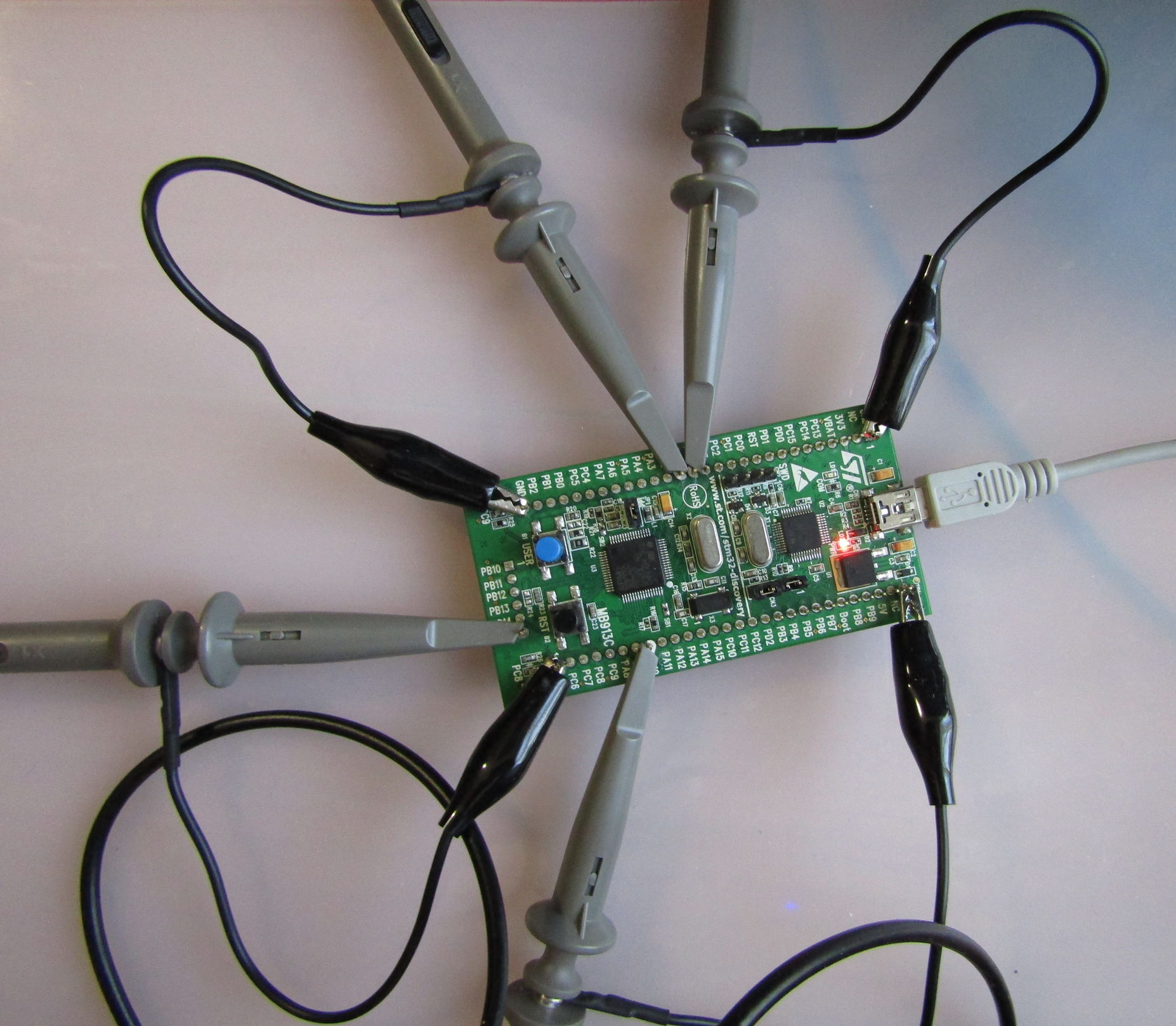
So we’ve probably come to the most important and interesting part. We have disassembled the physics of the process, the principle of operation seems to be clear, the necessary minimum of protection is also defined - it remains only to implement all this in real hardware. To do this, I use the STM32VL-Discovery shawl, I got it by the way back in 2011, at a time when ST distributed debugs at their conferences and since then she lay packed - opened the packaging just a couple of months ago, like the shelf life has not passed))) My “stand” for writing the code looks like this:
Now go through the connection. Since I need to form two signals with different frequencies, I had to use the PWM outputs on different timers. TIM1 generates a signal that sets the main frequency of 50 Hz and supplies them to transistors VT3 and VT4. The PIMA channel # 3 + its complementary output is used. Yes, yes, in STM32, hardware deadtime can only be configured between normal and complementary single-channel output, which I didn’t like much. The process of forming the sine itself is transmitted to the timer TIM2, there is no need for a delay here (previously wrote why), and it is quite suitable for generating a modulated signal on VT1 and VT2.
Used outputs:
- PA10 - normal PWM output, channel 3 of TIM1 timer, which generates 50 Hz per transistor VT3
- PB15 - complementary output of channel 3 of the timer TIM1, which is fed to the transistor VT4
- PA0 — №1 TIM2. VT1
- PA1 — №2 TIM2. VT2
The project is implemented in Keil 5, it will be attached to the archive at the end of the article. I don’t hope to tell how to create a project and similar obvious things, if such questions arise, I advise you to look at how to do it in Google or on youtube. All code is written in CMSIS (registers), because to use any additional levels of abstraction in the converter control system is simply a sin! In ST, these are SPL libraries and more current HALs. For interest I worked with those and with those, the conclusion is full of trash. HAL is so crazy in general, and for applications with hard real-time just doesn’t fit the word at all. In some critical moments, the registers were several times faster, by the way, I found more than one article on the Internet.
Some will surely ask: “Why not use DMA?” This can and should be done, but this article is more of an introductory nature, and the MC itself doesn’t do anything complicated in terms of computation, so the core performance isn’t exactly up to you. DMA is good, but you can do without DMA without any potential problems. Let's clarify what we need to do in the program:
- Create an array with our 240 sine points
- Adjust the clocking circuit at 24 MHz by selecting the source external quartz resonator
- Set the TIM1 timer to generate 50 Hz PWM with deadtime enabled
- Adjust TIM2 to generate PWM with 24 kHz carrier frequency
- Set the timer TIM6, which generates 24 kHz interrupts. In it, we will send the next value of the duty cycle from the table to the timer TIM2, as well as alternate the generation of half-waves
Nothing complicated, right? Then let's go ...
6.1. Create sine table
Everything is simple, just an array. The only thing to remember is that we have 120 points from 0 to 1000. We need to add 120 more points to the table, but in reverse order:
uint16_t sin_data[240] =
{13,26,39,52,65,78,91,104,117,130,143,156,169,182,195,207,220,233,246,258,
271,284,296,309,321,333,346,358,370,382,394,406,418,430,442,453,465,477,488,500,
511,522,533,544,555,566,577,587,598,608,619,629,639,649,659,669,678,688,697,707,
716,725,734,743,751,760,768,777,785,793,801,809,816,824,831,838,845,852,859,866,
872,878,884,891,896,902,908,913,918,923,928,933,938,942,946,951,955,958,962,965,
969,972,975,978,980,983,985,987,989,991,993,994,995,996,997,998,999,999,999,1000,
999,999,999,998,997,996,995,994,993,991,989,987,985,983,980,978,975,972,969,965,
962,958,955,951,946,942,938,933,928,923,918,913,908,902,896,891,884,878,872,866,
859,852,845,838,831,824,816,809,801,793,785,777,768,760,751,743,734,725,716,707,
697,688,678,669,659,649,639,629,619,608,598,587,577,566,555,544,533,522,511,500,
488,477,465,453,442,430,418,406,394,382,370,358,346,333,321,309,296,284,271,258,
246,233,220,207,195,182,169,156,143,130,117,104,91,78,65,52,39,26,13};
6.2. Setting the clocking system
Setting clocking in the STM32 is very flexible and convenient, but there are several nuances. The sequence itself looks like this:
1) Switch to clocking from the integrated RC-chain (HSI) to external quartz (HSE), then wait for the ready flag
RCC->CR |= ((uint32_t)RCC_CR_HSEON); 	// Enable HSE
while (!(RCC->CR & RCC_CR_HSERDY));	// Ready start HSE
2) The controller's flash memory is slightly slower than the kernel. For this, we configure flash clocking. If this is not done, the program will start, but will periodically fall: a pair of kW and unstable software are incompatible things.
FLASH->ACR = FLASH_ACR_PRFTBE | FLASH_ACR_LATENCY; // Cloclk Flash memory3) We set up dividers for the system bus clocking (AHB) and for the bus peripherals, of which there are already two pieces: APB1 and APB2. We need the maximum frequency, so we do not divide anything and the division factors are made equal to 1.
RCC->CFGR |= RCC_CFGR_HPRE_DIV1;	// AHB = SYSCLK/1
RCC->CFGR |= RCC_CFGR_PPRE1_DIV1;	// APB1 = HCLK/1
RCC->CFGR |= RCC_CFGR_PPRE2_DIV1;	// APB2 = HCLK/1
4) Adjust the frequency multiplier (PLL) predivider, which stands in front of him and divides the frequency of quartz by 2. We get that 8 MHz divided by 2 and received 4 MHz. Now we need to multiply them by 6, so that the output is 24 MHz. Before writing registers, we first erase their contents just in case.
RCC->CFGR &= ~RCC_CFGR_PLLMULL; // clear PLLMULL bits
RCC->CFGR &= ~RCC_CFGR_PLLSRC;	// clearn PLLSRC bits
RCC->CFGR &= ~RCC_CFGR_PLLXTPRE; // clearn PLLXTPRE bits

RCC->CFGR |= RCC_CFGR_PLLSRC_PREDIV1;  // source HSE
RCC->CFGR |= RCC_CFGR_PLLXTPRE_PREDIV1_Div2; // source HSE/2 = 4 MHz
RCC->CFGR |= RCC_CFGR_PLLMULL6; // PLL x6: clock = 4 MHz * 6 = 24 MHz
5) Now you need to turn on the frequency multiplier (PLL) and wait for the readiness flag:
RCC->CR |= RCC_CR_PLLON; // enable PLL
while((RCC->CR & RCC_CR_PLLRDY) == 0) {} // wait till PLL is ready
6) Finally, we configure the clock source for the system bus (AHB) output of our frequency multiplier, which has the cherished 24 MHz. Pre-register the contents of the clean, set the desired bit and wait for the ready flag:
RCC->CFGR &= ~RCC_CFGR_SW; // clear SW bits
RCC->CFGR |= RCC_CFGR_SW_PLL; // select source SYSCLK = PLL
while((RCC->CFGR & RCC_CFGR_SWS) != RCC_CFGR_SWS_1) {} // wait till PLL is used
As a result, we have this clocking setting function:
void RCC_Init (void){

RCC->CR |= ((uint32_t)RCC_CR_HSEON); // Enable HSE
while (!(RCC->CR & RCC_CR_HSERDY));   // Ready start HSE

FLASH->ACR = FLASH_ACR_PRFTBE | FLASH_ACR_LATENCY; // Cloclk Flash memory

RCC->CFGR |= RCC_CFGR_HPRE_DIV1; // AHB = SYSCLK/1
RCC->CFGR |= RCC_CFGR_PPRE1_DIV1; // APB1 = HCLK/1
RCC->CFGR |= RCC_CFGR_PPRE2_DIV1; // APB2 = HCLK/1

RCC->CFGR &= ~RCC_CFGR_PLLMULL; // clear PLLMULL bits
RCC->CFGR &= ~RCC_CFGR_PLLSRC; // clearn PLLSRC bits
RCC->CFGR &= ~RCC_CFGR_PLLXTPRE; // clearn PLLXTPRE bits

RCC->CFGR |= RCC_CFGR_PLLSRC_PREDIV1; // source HSE
RCC->CFGR |= RCC_CFGR_PLLXTPRE_PREDIV1_Div2; // source HSE/2 = 4 MHz
RCC->CFGR |= RCC_CFGR_PLLMULL6; // PLL x6: clock = 4 MHz * 6 = 24 MHz

RCC->CR |= RCC_CR_PLLON; // enable PLL
while((RCC->CR & RCC_CR_PLLRDY) == 0) {} // wait till PLL is ready
RCC->CFGR &= ~RCC_CFGR_SW; // clear SW bits
RCC->CFGR |= RCC_CFGR_SW_PLL; // select source SYSCLK = PLL
while((RCC->CFGR & RCC_CFGR_SWS) != RCC_CFGR_SWS_1) {} // wait till PLL is used
}
6.3. Setting the timer TIM1 and "dead time"
I will give a general setting of the timer, it is described in detail in the reference manual - I advise you to read the purpose of each register. And there are basic articles on working with PWM on the Internet. I have very well commented on the code itself, so I’ll quote immediately the code of the function for initializing the timer TIM1, and analyze the most interesting moments:
void PWM_50Hz_Init (void){

RCC->APB2ENR |= RCC_APB2ENR_TIM1EN; // enable clock for TIM1
RCC->APB2ENR |= RCC_APB2ENR_IOPAEN; // enable clock for port A
RCC->APB2ENR |= RCC_APB2ENR_IOPBEN; // enable clock for port B
RCC->APB2ENR |= RCC_APB2ENR_AFIOEN; // enable clock for alternative gpio

/****************************** Setting PA10 **************************************/

GPIOA->CRH 	&= ~GPIO_CRH_CNF10; // setting out alternative push-pull for PWM
GPIOA->CRH 	|= GPIO_CRH_CNF10_1;

GPIOA->CRH	&= ~GPIO_CRH_MODE10;
GPIOA->CRH	|= GPIO_CRH_MODE10; // gpio speed 50 MHz

/***************************** Setting PB15 ***************************************/

GPIOB->CRH 	&= ~GPIO_CRH_CNF15; // setting complementary for CH3N
GPIOB->CRH 	|= GPIO_CRH_CNF15_1;

GPIOB->CRH	&= ~GPIO_CRH_MODE15;
GPIOB->CRH	|= GPIO_CRH_MODE15; // gpio speed 50 MHz

/************************** Config PWM channel ************************************/

TIM1->PSC = 480-1; // div for clock: F = SYSCLK / [PSC + 1]
TIM1->ARR = 1000; // count to 1000
TIM1->CR1 &= ~TIM_CR1_CKD; // div for dead-time: Tdts = 1/Fosc = 41.6 ns
TIM1->CCR3 = 500; // duty cycle 50%

TIM1->CCER |= TIM_CCER_CC3E | TIM_CCER_CC3NE; // enable PWM complementary out
TIM1->CCER &= ~TIM_CCER_CC3NP; // active high level: 0 - high, 1 - low

TIM1->CCMR2 &= ~TIM_CCMR2_OC3M;
TIM1->CCMR2 |= TIM_CCMR2_OC3M_2 | TIM_CCMR2_OC3M_1; // positiv PWM

TIM1->BDTR &= ~TIM_BDTR_DTG; // clear register
TIM1->BDTR |= TIM_BDTR_DTG_2 | TIM_BDTR_DTG_1 | TIM_BDTR_DTG_0;	 // value dead-time
TIM1->BDTR |= TIM_BDTR_MOE | TIM_BDTR_AOE; // enable generation output

/*******************************************************************************/

TIM1->CR1 &= ~TIM_CR1_DIR; // count up: 0 - up, 1 - down
TIM1->CR1 &= ~TIM_CR1_CMS; // aligned on the front signal
TIM1->CR1 |= TIM_CR1_CEN; // start count

}
The duty cycle is fixed and never changes, as well as the frequency. It is this timer that sets the time and sequence of the diagonals:
TIM1->CCR3 = 500; // duty cycle 50%The duration of the pause "dead time" depends strongly on the TDTS time parameter, which is configured here:
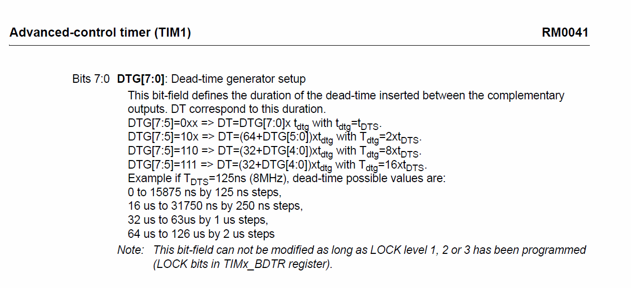
TIM1->CR1 &= ~TIM_CR1_CKD; // div for dead-time: Tdts = 1/Fosc = 41.6 nsIts duration is 1 clock tick. If you look in the reference manual, you can see that the CKD bits can, for example, make Tdts equal to 2, 8 ticks, and so on.
The very same pause time is set here:
TIM1->BDTR |= TIM_BDTR_DTG_2 | TIM_BDTR_DTG_1 | TIM_BDTR_DTG_0;If you open the reference manual RM0041, you will see formulas for calculating DT. As you can see the Tdts parameter is fundamental there:
6.4. Setting the timer TIM2, forming a sine
It’s still easier here, probably there’s no point in explaining something in the setup, for comments are already redundant. If you have questions - wait for them in the comments.
void PWM_Sinus_Init (void){
RCC->APB1ENR |= RCC_APB1ENR_TIM2EN; // enable clock for TIM2
RCC->APB2ENR |= RCC_APB2ENR_IOPAEN; // enable clock for port A
RCC->APB2ENR |= RCC_APB2ENR_AFIOEN; // enable clock for alternative gpio

/****************************** Setting PA0 ***************************************/

GPIOA->CRL 	&= ~GPIO_CRL_CNF0; // setting out alternative push-pull for PWM1_CH1
GPIOA->CRL 	|= GPIO_CRL_CNF0_1;

GPIOA->CRL	&= ~GPIO_CRL_MODE0;
GPIOA->CRL	|= GPIO_CRL_MODE0; // gpio speed 50 MHz
/****************************** Setting PA1 ***************************************/

GPIOA->CRL 	&= ~GPIO_CRL_CNF1; // setting out alternative push-pull for PWM1_CH1
GPIOA->CRL 	|= GPIO_CRL_CNF1_1;

GPIOA->CRL	&= ~GPIO_CRL_MODE1;
GPIOA->CRL	|= GPIO_CRL_MODE1; // gpio speed 50 MHz

/*************************** Config PWM channel ***********************************/

TIM2->PSC = 0; // div for clock: F = SYSCLK / [PSC + 1]
TIM2->ARR = 1000; // count to 1000
TIM2->CCR1 = 0; // duty cycle 0%
TIM2->CCR2 = 0; // duty cycle 0%

TIM2->CCER |= TIM_CCER_CC1E; // enable PWM out to PA8
TIM2->CCER &= ~TIM_CCER_CC1P; // active high level: 0 - high, 1 - low

TIM2->CCER |= TIM_CCER_CC2E; // enable PWM complementary out to PA9
TIM2->CCER &= ~TIM_CCER_CC1P; // active high level: 0 - high, 1 - low

TIM2->CCMR1 &= ~(TIM_CCMR1_OC1M | TIM_CCMR1_OC2M);
TIM2->CCMR1 |= TIM_CCMR1_OC1M_2 | TIM_CCMR1_OC1M_1 |
 TIM_CCMR1_OC2M_2 | TIM_CCMR1_OC2M_1; // positiv PWM1_CH1 and PWM1_CH2

/*******************************************************************************/

TIM2->CR1 &= ~TIM_CR1_DIR; // count up: 0 - up, 1 - down
TIM2->CR1 &= ~TIM_CR1_CMS; // aligned on the front signal: 00 - front; 01, 10, 11 - center
TIM2->CR1 |= TIM_CR1_CEN; // start count

}
6.5. Setting the TIM6 Timer Interrupt
We configure the timer itself at a frequency of 24 kHz:
void TIM6_step_init (void){

RCC->APB1ENR |= RCC_APB1ENR_TIM6EN; // enable clock for basic TIM6

TIM6->PSC = 1-1; // div, frequency 24 kHz
TIM6->ARR = 1000; // count to 1000
TIM6->DIER |= TIM_DIER_UIE; // enable interrupt for timer
TIM6->CR1 |= TIM_CR1_CEN; // start count

NVIC_EnableIRQ(TIM6_DAC_IRQn); // enable interrupt TIM6_DAC_IRQn

}
6.6. Implementation of the main control algorithm
Major events occur in an interrupt generated by the TIM6 timer. An interrupt is generated every 41.66 μs, if you remember this is our sample rate. Accordingly, in the interrupt, the value of the duty ratio from the table to the CCRx register is written . Also in this interrupt, it is determined which diagonal is currently drawn by inverting the sin_status flag after each half period. We draw 240 points, invert the flag, which causes the control to switch to another channel, when it has already drawn, the flag is inverted again and everything repeats. Main algorithm code:
void TIM6_DAC_IRQHandler(void){

TIM6->SR &= ~TIM_SR_UIF;

if(sin_status == 0){TIM2->CCR1 = sin_data[sin_step];}
if(sin_status == 1){TIM2->CCR2 = sin_data[sin_step];}

sin_step++;

if(sin_step >= 240){
         sin_step=0;
         sin_status = sin_status ? 0 : 1;
         }
}
Results
Download the project, compile and upload to your microcontroller and get a working inverter. All you have to do is make a bridge and give signals to it:
I’ve put some of my bridge schemes in PDF earlier in the PDF, I hope it will help you in mastering power electronics.
Also in the project, I pulled FreeRTOS. Of course, using RTOS means it is impossible to implement similar management tasks, since simple switching between tasks lasts from 4 to 18 microseconds, and that if the code is well written and nothing can hinder the work of the scheduler. This does not allow to get a control system operating in hard real-time. I set up FreeRTOS for another: communication interfaces (RS-485 Modbus RTU), adjustment of the output voltage amplitude, recalculation of the table, synchronization with the 230V network and so on. I will also try to implement all these buns on STM32, and maybe I'll write a continuation of the topic of the article, if interesting results are obtained and there is something to share.
I hope you liked the article. If you have questions on the use of this code in real hardware, I will be glad to answer them. Also, please do not take this code as something ready, this is the core of the converter that implements the main function. All the "buns" and other redundancy you can add yourself. The bare core of the project will allow you to understand how it works and not spend a lot of time disassembling code.
Materials
UPD1: I would like to thank the sleip user for a number of errors found, mainly in the sine table - it has been changed. Those who have used the code or the table itself, please copy it again, in the article already corrected version.
Source: https://habr.com/ru/post/358172/
All Articles