On power up
And an amazing story happened to me, which, if it were written with silver needles in the corners of the eyes, would serve as an edification for those who learn.
This story began with the design of a portable device, in which it was desirable to reduce battery consumption in off mode, but the mechanical switch was unacceptable due to design features. It was also undesirable to use the transistor as a key due to the significant operating currents of the device (more than 3A). Therefore, a widespread decision was made to block the operation of the power sources (PIs) that make up the device by controlling the work permit signal. Nothing new or unusual, such schemes can be found 12 to a dozen in devices with autonomous power, however, quite unexpectedly, certain complications arose, which led to a number of instructive conclusions.
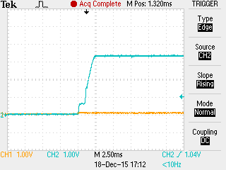
To begin with, I will give a scheme, which will be discussed further, it is presented in a simplified version.
Everything is simple here - in the initial state there is a main voltage of 5 volts (battery), but the power sources are turned off, which is provided by the resistor R2. In this case, the power sources consume a rest current from the main source, which is quite small (in this case, 2 μA + 2 * 1 μA = 4 μA. To turn on, press the S1 button, the voltage from the main source through diodes D3 and D2 goes to the enabling inputs of the PI, which are turned on and start generating the required voltages, including the 3.3 V power supply for the MK. The MK starts up, starts the program and sets a high level on the corresponding pin, which through the diode D1 additionally enables the operation of the power supply. From this point on, you can release the S button 1, the further work of the PI is provided by the output of the MK until the decision is made to disconnect and the MK does not remove the high potential from the diode D1, then the PI will stop working and we will return to the initial state.
')
This scheme was implemented, tested, and proved to be quite workable. It has its pitfalls associated with the chattering of the S1 key, but in this case it is not about them.
Surprises awaited us elsewhere. The fact is that the applied MK has a built-in loader through the UART, and for its use an additional switching mode was implemented using auxiliary MK outputs. From the point of view of the power management scheme, the peculiarity of this mode was that the corresponding output was not involved in the loader program, all outputs after the initial reset should be in the high-impedance (third) state, therefore, when the S1 key is depressed, the device must be powered off ( R2 is provided, which is essential to prevent the MK from hanging in case of an unforeseen entry into the programming mode (the output from the boot program without connecting a programming device to this MK was not implemented van).
However, the reality overturned the rainbow plans, after releasing the S1 button, the device remained on. We start the search for a malfunction: first, we unsolder the diode D1 and make sure that the shutdown happens - it means that the power-on hold signal comes from the MC (well, yes, there is nowhere else, but you never know).
We suggest that the leakage current of the output is enough to create a voltage across the resistor R2, change it to the nominal 10 kΩ, the phenomenon does not disappear. The calculation shows that the leakage current must be at least 0.3mA, which clearly exceeds the leakage by specifications by orders of magnitude. We change the nominal to 1 kOhm, the device starts to turn off, this means that the current from the output of the MC does not exceed 3 mA. In principle, the scheme has earned and you can do other things, but the spirit of research calls to figure out where such a large current comes from on the disconnected output (of course, it is not that big, but it exceeds the data of TU - 1 μA by orders of magnitude).
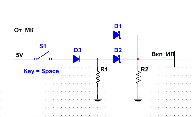
We measure the outgoing current of the other outputs in the third state and make sure that everything is within the limits of the specifications, that is, not more than 1 μA. We return the old face value and try to measure the current at this output of the MK, and here the misunderstandings begin. As soon as we touch the device probe (portable, by the way, that is, without communication with the network) to this MK pin, the device immediately turns off, and the second probe of the device dangles in the air. If we look with an oscilloscope, we see a high level of approximately 3.3V. This behavior of the MC leads to certain suspicions, and to check them we connect an ammeter parallel to the diode D1. And we observe that when the S1 button is pressed, 300 μA flows into the MK, but when it is released, the device turns off, that is, the device continues to influence the situation.
There is an assumption that we are dealing with the so-called “thyristor snapping-in” CMOS structures, which spoiled a lot of blood for developers, but went into non-existence along with the 564 series. But unlike those snaps, which led to a significant through-current, this snapping is weak and may be disturbed even by a slight change in the capacitance connected to the output. The main condition for snapping is the excess voltage at the chip output over the supply voltage. To check this fact, we remove the voltage waveform at this output of the MK (yellow color) together with the supply voltage of the MK (blue color) in the process of switching on.
And precisely, we observe the confirmation of this hypothesis - the voltage at the MK output stably exceeds the supply voltage until a certain moment, apparently, at this moment the snapping-in occurs.
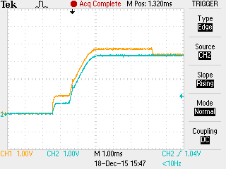
From where we can get an excess at the MK input - the answer is simple: from the main power source through the reverse-offset diode D1. Let us test this hypothesis, for which we connect in series with the diode D2 a resistor of 2/3 of R2, then we limit the voltage at the control point to less than 3 V, and accordingly, we limit the excess over the power supply of the MC. We receive the following oscillogram.
It is seen that our assumption was confirmed, the excess occurs only up to the 3V supply value and the device starts to turn off stably when the S1 button is released. Again, everything is good, the problem is solved, but still we have moments when the voltage at the output exceeds the supply voltage, and I would like to avoid this situation - we have already received an incomprehensible snap once, who knows when it will come out.
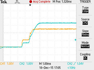
We install a 10kΩ resistor at the MK input and connect it to ground. The oscillogram shows that there is no excess voltage over the power supply (in fact, it is and is about 100 mV, but we believe that it does not exist).
From here, it is possible to calculate the current flowing through the reverse-biased diode D1 - about 10 μA, which correlates well with the value from TU - no more than 500 μA at a voltage of -20 V (we have-5 V).
How can we reduce this current? It is enough to replace the Schottky diode with a conventional one and, even with old resistor values, the device begins to turn off stably. Well, not surprisingly, since a normal diode has a reverse current of no more than 25nA with the same -20V.
However, just in case, we do everything possible: we change the Schottky diode to a normal one, reduce the R2 nominal to 10k ohm, install a 6.8k ohm resistor in series with the D2 diode, install a 10k ohm resistor between the output and ground of the MK, and make sure that the device stably turns off.
We summarize - the incorrect behavior of the device was caused by the latching state of the MK output caused by the supply of an external voltage source exceeding the supply voltage of the MK through the reverse-biased Schottky diode due to its high (compared to a conventional diode but strictly within the DUT) leakage current.
Why the Schottky diodes were initially chosen because of the low fall in the forward direction, although it was possible to open the specifications for the power supplies and see that for them the high level is 1.2V, which is also well achieved by conventional diodes (3.3-0.7> 1.2). In this case, the habit of minimizing the fall on the diodes and, accordingly, the heat dissipation on them, played a cruel joke with the author.
Why the conclusion of the MC went into a latched state, and at some incomprehensible moment, the author does not know, this is surely some kind of technological feature, but in any case the author does not have any complaints about the developers of MC, for the
Source: https://habr.com/ru/post/357928/
All Articles