Implementing FizzBuzz on FPGA
Recently, I became interested in FPGA programming and decided that it would be interesting to implement the algorithm of the FizzBuzz game on FPGA. FPGA ( user-programmable gate array ) is an interesting chip. It is programmed to execute arbitrary digital logic. It is possible to construct a complex circuit without laying the physical channels between the individual valves and the flip-flops. The microcircuit can turn into anything from a logic analyzer to a microprocessor and a video generator.
Test FizzBuzz - write a program that gives numbers from 1 to 100, where multiples of three are replaced by the word “Fizz”, multiples of five by the word “Buzz”, and multiples of fifteen by “FizzBuzz”. Since such a program is implemented in several lines of code, it is often asked at interviews in order to weed out those who do not know how to program at all.
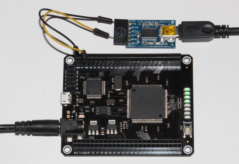
A Mojo FPGA card connected to the serial-to-USB port. The big chip on the board is the Spartan 6 FPGA
')
The implementation of FizzBuzz in digital logic, not in code, is rather meaningless, but it seemed to me a good example for learning. one For this project, I used a simple Mojo V3 FPGA development board for beginners. It has the FPGA of the Xilinx Spartan 6 family. It is one of the smallest FPGAs, but it has 9000 logic cells and 11,000 triggers - so the kid is capable of a lot.
What does it mean to implement FizzBuzz on FPGA? This means that the contacts of the general-purpose input / output interface (GPIO) from the board can be connected to anything, so the FizzBuzz output will appear in a different form: by LEDs, on seven-segment indicators, LCD display, VGA monitor. I decided that text output to the terminal via a serial channel most closely matches the spirit of the “standard” FizzBuzz program. So the first thing to do is to implement serial output on the FPGA.
The main idea of serial communication is the transmission of bits one by one. The RS-232 serial port is a simple protocol for serial data transmission, invented in 1960 to connect teletypes and modems. The diagram below shows how the “F” symbol (binary 01000110) is sequentially transmitted over the channel. First, the start bit (zero) is sent to indicate the beginning of a character. 2 Then eight bits of the character are transmitted in reverse order. At the end, a stop bit is sent. Between the characters, the bar remains in standby mode (one) until the next character is transmitted. At a baud rate of 9600 baud, the transmission of each bit takes 1/9600 seconds. With eight data bits with no parity and one stop bit, this protocol is known as 8N1. There are many protocols for serial data transmission, but 9600 8N1 is very common.

Sequential transmission of the character “F” at 9600 baud / 8N1
The first step in implementing such a serial transmission is to create 1/9600 second intervals for each bit. This interval is measured by calculating 5208 clocks on a Mojo. 3 I made a 13-bit counter for periodic counting from 0 to 5207. A simple finite state machine keeps track of which bit is output in each interval. It starts with the initial bit, changes its state as it processes the eight bits of data and the stop bit. The state is stored in a four-bit register (in general, in FPGA you will have to deal with a large number of clock pulses, counters and finite automata).
To create an interval and state registers in the FPGA, I wrote code in the Verilog hardware description language. I will not explain in detail Verilog - I hope you will understand how it works. In the following code, the first lines specify the 13-bit
Although it looks like ordinary program code, it works completely differently. In a conventional programming language, operations are usually performed sequentially, since the program is executed line by line. For example, the processor checks the value of
The next part of the code outputs the corresponding bit for each state. As before, it looks like a normal program code, but generates hardware circuits, and not operations that are performed sequentially. In this case, the code creates a logic gate (essentially a multiplexer) to select the right
There is some more code to set constants, initialize counters, start and stop the transmission of each character, but the code above gives a general idea of how Verilog works. All code for serial data output is here .
The next step is to determine what specifically to send through the serial channel. How to translate numbers from 1 to 100 in ASCII characters? This is trivial on a microprocessor, but difficult in digital logic. The problem is that converting a binary number to a decimal requires dividing by 10 and 100, and the division is very inconvenient to implement in the gates. I decided to use
binary decimal counter (BCD), which stores each of the three digits separately. This made the meter a bit more complicated, since nodes are introduced into the counter circuit, which ensure the correction of the counting process in case of overflow to one side or the other from the nine. But the issuance of numbers is simplified.
I wrote a BCD module ( source code ) for a three-digit counter. It has three four-bit counters
As before, keep in mind that this only looks like a normal program, but in reality the code turns into a bunch of logic gates that generate new values of
The next task is to check the divisibility by 3 and 5. As a simple division, division with the remainder is also easy to implement on a microprocessor, but difficult in digital logic. There is no built-in division operation, so you have to create a whole bunch of gates. Although the IDE can synthesize them for division with the remainder, but it is tasteless. Instead, I just made counters for the remainder of the division by 3 and 5. For example, mod3 will simply give out 0, 1, 2, 0, 1, 2 ... 5
The last part of FizzBuzz is the code for outputting each line character by character. In the program, we can simply call the sequential output procedure for each character. But in the FPGA, you need to keep track of which symbol is sent to the output, with the help of another state machine. Note that when converting each digit to ASCII, binary 11 is concatenated using a slightly odd syntax of
If you put it all together, the final FizzBuzz scheme consists of numerous state machines and counters. The main state machine controls the code at the top, moving through the characters in the string. For each character, the state machine activates the serial output module and waits for the character to be output. Inside the module, the state machine passes through each bit of the symbol. It waits until the data rate counter counts the bit width. When the symbol transfer is complete, the serial output module sends a signal to the master state machine. Then it goes to the next character in the string. When the line is completed, the main state machine increases the BCD counter (which counts from 1 to 100) - and starts outputting the next line.
In programming languages, it is easy to perform sequential operations, cycles, subroutine calls, and so on. But in FPGA, you need to explicitly track what is happening with the help of finite automata and counters. In exchange, FPGA provides powerful concurrency and control.
To compile Verilog code, I used the Xilinx ISE tool (see below). In this development environment, you can write code, model it, and synthesize logic circuits for downloading to FPGA. The ISE tool is pretty straightforward and is explained in the Mojo manuals . The synthesis process is much slower than compiling: for my FizzBuzz program, it took about 45 seconds.

By writing the Verilog code in the Xilinx ISE tool, you can program the FPGA functionality
As soon as my code earned in simulator 7 I downloaded it to the FPGA board via USB cable. I connected the FPGA output pin to the USB-to-serial 6 adapter and used a terminal emulator (

The first page of the FizzBuzz FPGA output in the terminal emulator
The image below shows raw raw serial data from an FPGA (yellow). This is the end result of the operation of the FizzBuzz scheme on the FPGA board - a sequence of pulses. The oscilloscope also demonstrates decoded ASCII characters (green). The image shows FizzBuzz for 2, 3, and 4 (CR and LF are carriage return and line feed characters).

The serial output signal (yellow) at the beginning of the FizzBuzz output. ASCII decoding - green
You may ask how the Verilog schema description is converted to digital logic and how the FPGA implements this logic. The ISE synthesis tool takes a description of Verilog — and generates schemas suitable for implementation inside an FPGA. First, from the Verilog code, it synthesizes a “netlist” (netlist), defining logic and interconnections. Then translates the lists into FPGA primitives in accordance with the capabilities of a particular chip (in our case Spartan 6). At the end, an optimization procedure is started to minimize the signal path.
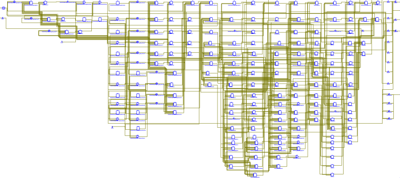
FizzBuzz circuit diagram
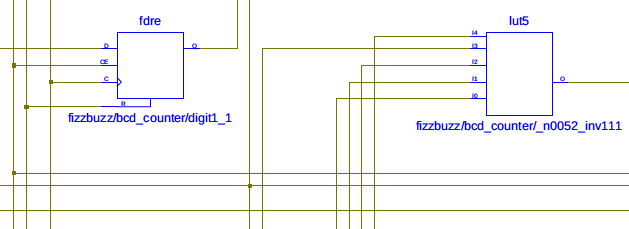
The figure above shows the FizzBuzz chain as generated by the synthesis tool. As you can see, the Verilog code turns into a big tangle of schemes. Each block is a trigger, logic element, multiplexer, or other element. The blocks consist of counters, status registers and logic of the FizzBuzz circuit. Although it seems that there are a lot of logical elements, in fact, less than 2% of the power of the chip is used. A close-up (below) shows the trigger scheme (labeled “fdre”) 8 and a lookup table (labeled “lut5”) from the BCD counter. What is convenient in Verilog is that you design the circuit at a high level — and it turns into a low-level circuit. This is called RTL ( register transfer level ) and allows the use of registers and high-level operations on them without worrying about low-level hardware implementation. For example, you can simply write
Detailed diagram of the trigger and search table
The FPGA uses an interesting technique for logical equations. Instead of linking individual gates, a lookup table (LUT) is used, with which it is convenient to implement arbitrary logic. Each table has six input lines, so it can implement any combinatorial logic with six input signals. It turns out 64 different combinations of input signal and 64-bit truth table. By saving this table as a 64-bit image, LUT can implement any logical function.
For example, part of the logic for an output pin is equivalent to the logic below. It is implemented by storing the 64-bit value

Logic elements implemented by a single lookup table in FPGA
The last part of the task is a matrix switch that arbitrarily connects the circuits. In Spartan 6, several LUTs, triggers, and multiplexers are assembled into configurable logic blocks (CLB) 9 . These CLBs are connected by matrix switches , as shown below. Each block of the matrix switch is programmed to connect different buses, which allows you to lay the FPGA contacts as you like. An important part of the FPGA synthesis process is block positioning to minimize wiring distance. This is necessary both to minimize the propagation delay of the signal, and to maintain a reserve of interconnect paths.

The matrix switch in the Spartan 6 FPGA allows arbitrary connections between CLBs. From the user manual
Personally, I first looked at the FPGAs with fear, because they seemed scary and strange. Although there is a learning curve, but FPGAs were not as complex as I thought. If you are interested in new programming paradigms, then the FPGA will certainly show things from a different angle. What you take for granted, such as the sequential execution of operations, will come to the fore. You can experiment with high parallelism. And the FPGA will allow you to better understand how digital circuits work.
However, I would not recommend experimenting with FPGA if you are at least somewhat familiar with connecting LEDs / switches and do not understand basic digital logic: gates, triggers, and state machines. But if you are comfortable with Arduino, then FPGA is the smart next step.
Probably, for most applications the microcontroller is better suited to FPGA, and it is easier to program. If you don’t need a high data transfer rate or concurrency, then FPGA will probably be redundant. In my case, the microcontroller barely coped with the three megabit Ethernet gateway , so for the next project I take a closer look at the FPGA.
Mojo FPGA development boards sell Adafruit and Sparkfun , so I thought it was a good hacker choice. The board is designed for beginners in FPGA programming, and it copes well with this role. The creators of Mojo have written a large collection of guides for using Verilog . ten . If the manual is written for a specific board, then problems with the board and tools are solved much faster. Mojo is programmed with a standard USB cable - this is more convenient than special JTAG adapters.
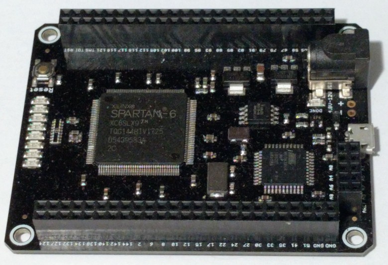
Mojo FPGA board with Spartan-6 FPGA chip
Although there are many I / O pins on the Mojo, no peripherals are sold with it, except for eight LEDs. It would be more pleasant to experiment with the board, if there are buttons, seven-segment displays, VGA output, sensors, and so on. (They are easy to connect to Mojo, but it would be convenient to have it included). In addition, some development boards have external RAM, and Mojo does not. This is a problem for applications like a logic analyzer that requires a lot of memory. eleven (Although you can extend Mojo with IO lining or RAM lining ).
A good book to get started with Mojo is “FPGA Programming . ” It also describes the much cheaper Papilo One and Elbert 2 motherboards. If you want to see other options, here is a list of FPGA development boards .
The task of FizzBuzz is impractical to implement on FPGA, but it was interesting, I learned a lot about FPGA programming. But of course, I won’t get a job if the FizzBuzz question is asked for an interview! My code is on GitHub , but keep in mind that I'm still new to this business.
1. Implementing a microprocessor on an FPGA is a trivial task. For example, with the Spartan 6 chip, you can click a couple of buttons in the IDE wizard - and it will generate a circuit for the MicroBlaze processor . Therefore, an intelligent person would write FizzBuzz code in a few lines of C, and then run it on the processor inside the FPGA. But for me it is too easy. ↑
2. The start bit is required, otherwise the receiver will not be able to determine the beginning of the character if the first bit of the character is 1.
3. Since in Mojo the clock frequency is 50 MHz, then at 9600 baud each bit will take 50000000/9600 or approximately 5208 cycles. This is not a very high speed, so for the experiment I ran the code at a speed of 10 million baud (counting up to five cycles for each bit) - and the circuit survived (the USB-to-serial interface only supports speed up to 230400 baud, so I checked the result on the oscilloscope). ↑
4. In Verilog,
5. I used not a binary, but a binary-decimal counter, so the remainder of the division by 5 is determined almost trivially, looking at the last digit. But the remainder of the division by 3 is non-trivial, so I had to leave the counter option. ↑
6. It was impossible to send serial input directly to the computer, because it does not have a serial port. Instead, I used the USB-to-serial adapter , FTDI Friend from Adafruit. This adapter can also accept a 3.3-volt signal, in contrast to the inconvenient +/− 15 volts in the original RS-232. ↑
7. Debugging FPGA is completely different from debugging a program. Since the FPGA is essentially a black box, you first need to check everything in the simulator, otherwise you will go to the "FPGA-hell" with blinking LEDs, trying to understand what is happening.In the process of debugging, to simulate a circuit, you need to write a “testbench” (testbench) - the Verilog code, which at different times provides different input data ( example ). Then run the simulator (below) and check that the output is correct. Xilinx's ISim simulator allows you to check the FPGA circuit. If something goes wrong, the simulator lets you go over the internal signals and identify the problem. After complete testing in the simulator when running on a real FPGA, my code has only the most trivial problems. The main one was that I assigned a serial output to the wrong contact, so there was no output.

↑
8. Spartan 6 FPGA supports several types of triggers. FDRE is a D-flip-flop with a synchronous reset / set-up input and clock operation. ↑
9. Configurable Spartan 6 FPGA (CLB) logic blocks are quite complex. They contain LUT modules, 8 flip-flops, wide multiplexers, logic, distributed RAM, and shift registers. The hard-soldered components of these blocks slightly reduce flexibility, but greatly simplify the design of the matrix switches. CLB is described in detail in the CLB User Guide . There are other types of blocks in the Spartan 6 FPGA, including clock generation units and DSP units capable of fast multiplication of 18 × 18 bits. ↑
10. An alternative to the Verilog language is VHDL , which is also supported by the development environment. Mojo also supports Lucid , a simpler FPGA language, developed by the Mojo team. Mojo Lucid Guides explain the language, and there is also a book on this topic. However, I decided that it is better to learn the standard language than Lucid. ↑
11. Mojo does not have external RAM, but there are 576 kilobits of internal memory. Although this is a tiny amount compared to boards that have megabytes of external DRAM. ↑
Test FizzBuzz - write a program that gives numbers from 1 to 100, where multiples of three are replaced by the word “Fizz”, multiples of five by the word “Buzz”, and multiples of fifteen by “FizzBuzz”. Since such a program is implemented in several lines of code, it is often asked at interviews in order to weed out those who do not know how to program at all.
A Mojo FPGA card connected to the serial-to-USB port. The big chip on the board is the Spartan 6 FPGA
')
The implementation of FizzBuzz in digital logic, not in code, is rather meaningless, but it seemed to me a good example for learning. one For this project, I used a simple Mojo V3 FPGA development board for beginners. It has the FPGA of the Xilinx Spartan 6 family. It is one of the smallest FPGAs, but it has 9000 logic cells and 11,000 triggers - so the kid is capable of a lot.
Implementing FPGA serial output
What does it mean to implement FizzBuzz on FPGA? This means that the contacts of the general-purpose input / output interface (GPIO) from the board can be connected to anything, so the FizzBuzz output will appear in a different form: by LEDs, on seven-segment indicators, LCD display, VGA monitor. I decided that text output to the terminal via a serial channel most closely matches the spirit of the “standard” FizzBuzz program. So the first thing to do is to implement serial output on the FPGA.
The main idea of serial communication is the transmission of bits one by one. The RS-232 serial port is a simple protocol for serial data transmission, invented in 1960 to connect teletypes and modems. The diagram below shows how the “F” symbol (binary 01000110) is sequentially transmitted over the channel. First, the start bit (zero) is sent to indicate the beginning of a character. 2 Then eight bits of the character are transmitted in reverse order. At the end, a stop bit is sent. Between the characters, the bar remains in standby mode (one) until the next character is transmitted. At a baud rate of 9600 baud, the transmission of each bit takes 1/9600 seconds. With eight data bits with no parity and one stop bit, this protocol is known as 8N1. There are many protocols for serial data transmission, but 9600 8N1 is very common.
Sequential transmission of the character “F” at 9600 baud / 8N1
The first step in implementing such a serial transmission is to create 1/9600 second intervals for each bit. This interval is measured by calculating 5208 clocks on a Mojo. 3 I made a 13-bit counter for periodic counting from 0 to 5207. A simple finite state machine keeps track of which bit is output in each interval. It starts with the initial bit, changes its state as it processes the eight bits of data and the stop bit. The state is stored in a four-bit register (in general, in FPGA you will have to deal with a large number of clock pulses, counters and finite automata).
To create an interval and state registers in the FPGA, I wrote code in the Verilog hardware description language. I will not explain in detail Verilog - I hope you will understand how it works. In the following code, the first lines specify the 13-bit
counter register and the four-bit state register. The counter is increased to a value of 5207, then reset to 0, while the state incremented by one to process the next output bit. (Note that <= is an assignment operator, not a comparison 4 ). The string always @(posedge clk) indicates that the procedural block is triggered on the positive edge of the clock frequency. reg [12:0] counter; reg [3:0] state; always @(posedge clk) begin if (counter < 5207) begin counter <= counter + 1; end else begin counter <= 0; state <= state + 1; end end Although it looks like ordinary program code, it works completely differently. In a conventional programming language, operations are usually performed sequentially, since the program is executed line by line. For example, the processor checks the value of
counter . Then adds one to the counter . But in Verilog there is neither a processor nor an executable program. Instead, the code creates the hardware to perform the operations. For example, to increase the counter , one addition scheme is created, and for increasing the state , another scheme is created. Additional logic is created for comparison with 5207. Unlike a serial processor, an FPGA performs everything in parallel. For example, an FPGA simultaneously performs a comparison of 5207, an increase and a reset counter , and an increase in state on each clock. Because of this, in strongly parallel tasks, FPGA can work to be much faster than a processor.The next part of the code outputs the corresponding bit for each state. As before, it looks like a normal program code, but generates hardware circuits, and not operations that are performed sequentially. In this case, the code creates a logic gate (essentially a multiplexer) to select the right
out value. case (state) IDLE: out = MARK; // high START: out = SPACE; // low BIT0: out = char1[0]; BIT1: out = char1[1]; ... BIT6: out = char1[6]; STOP: out = MARK; default: out = MARK; endcase There is some more code to set constants, initialize counters, start and stop the transmission of each character, but the code above gives a general idea of how Verilog works. All code for serial data output is here .
FizzBuzz Algorithm
The next step is to determine what specifically to send through the serial channel. How to translate numbers from 1 to 100 in ASCII characters? This is trivial on a microprocessor, but difficult in digital logic. The problem is that converting a binary number to a decimal requires dividing by 10 and 100, and the division is very inconvenient to implement in the gates. I decided to use
binary decimal counter (BCD), which stores each of the three digits separately. This made the meter a bit more complicated, since nodes are introduced into the counter circuit, which ensure the correction of the counting process in case of overflow to one side or the other from the nine. But the issuance of numbers is simplified.
I wrote a BCD module ( source code ) for a three-digit counter. It has three four-bit counters
digit2 , digit1 , and digit0 . The increment flag signals an increase in the counter. Usually, only digit0 increases. But if it reaches nine, it turns to 0, and digit1 increases. If digit1 also becomes 9, then it turns to 0, and digit2 increases. Thus, there is a countdown from 000 to 999. if (increment) begin if (digit0 != 9) begin // Regular increment digit 0 digit0 <= digit0 + 1; end else begin // Carry from digit 0 digit0 <= 0; if (digit1 != 9) begin // Regular increment digit 1 digit1 <= digit1 + 1; end else begin // Carry from digit 1 digit1 <= 0; digit2 <= digit2 + 1; end end end As before, keep in mind that this only looks like a normal program, but in reality the code turns into a bunch of logic gates that generate new values of
digit2 , digit1 and digit0 on each digit0 . The system does not follow the instructions in order, so performance is not limited by the number of instructions, but only by delaying the signals propagating through the valves.The next task is to check the divisibility by 3 and 5. As a simple division, division with the remainder is also easy to implement on a microprocessor, but difficult in digital logic. There is no built-in division operation, so you have to create a whole bunch of gates. Although the IDE can synthesize them for division with the remainder, but it is tasteless. Instead, I just made counters for the remainder of the division by 3 and 5. For example, mod3 will simply give out 0, 1, 2, 0, 1, 2 ... 5
The last part of FizzBuzz is the code for outputting each line character by character. In the program, we can simply call the sequential output procedure for each character. But in the FPGA, you need to keep track of which symbol is sent to the output, with the help of another state machine. Note that when converting each digit to ASCII, binary 11 is concatenated using a slightly odd syntax of
2'b11 . The code given here is a bit simplified. The full code contains zero checks at the beginning, so “001” is output as “1”. state <= state + 1; // Different state from serial if (mod3 == 0 && mod5 != 0) begin // Fizz case (state) 1: char <= "F"; 2: char <= "i"; 3: char <= "z"; 4: char <= "z"; 5: char <= "\r"; 6: begin char <= "\n"; state <= NEXT; // Done with output line end endcase end else if (mod3 != 0 && mod5 == 0) begin ... Buzz case omitted ... end else if (mod3 == 0 && mod5 == 0) begin ... Fizzbuzz case omitted ... end else begin // No divisors; output the digits of the number. case (state) 1: char <= {2'b11, digit2[3:0]}; 2: char <= {2'b11, digit1[3:0]}; 3: char <= {2'b11, digit0[3:0]}; 4: char <= "\r"; 5: begin char <= "\n"; state <= NEXT; end endcase end If you put it all together, the final FizzBuzz scheme consists of numerous state machines and counters. The main state machine controls the code at the top, moving through the characters in the string. For each character, the state machine activates the serial output module and waits for the character to be output. Inside the module, the state machine passes through each bit of the symbol. It waits until the data rate counter counts the bit width. When the symbol transfer is complete, the serial output module sends a signal to the master state machine. Then it goes to the next character in the string. When the line is completed, the main state machine increases the BCD counter (which counts from 1 to 100) - and starts outputting the next line.
In programming languages, it is easy to perform sequential operations, cycles, subroutine calls, and so on. But in FPGA, you need to explicitly track what is happening with the help of finite automata and counters. In exchange, FPGA provides powerful concurrency and control.
Running FizzBuzz on the FPGA board
To compile Verilog code, I used the Xilinx ISE tool (see below). In this development environment, you can write code, model it, and synthesize logic circuits for downloading to FPGA. The ISE tool is pretty straightforward and is explained in the Mojo manuals . The synthesis process is much slower than compiling: for my FizzBuzz program, it took about 45 seconds.
By writing the Verilog code in the Xilinx ISE tool, you can program the FPGA functionality
As soon as my code earned in simulator 7 I downloaded it to the FPGA board via USB cable. I connected the FPGA output pin to the USB-to-serial 6 adapter and used a terminal emulator (
screen ) to display the serial output on the computer. I pressed the reboot button on the Mojo board - and (after a little extra debugging) the output of FizzBuzz appeared (below).The first page of the FizzBuzz FPGA output in the terminal emulator
The image below shows raw raw serial data from an FPGA (yellow). This is the end result of the operation of the FizzBuzz scheme on the FPGA board - a sequence of pulses. The oscilloscope also demonstrates decoded ASCII characters (green). The image shows FizzBuzz for 2, 3, and 4 (CR and LF are carriage return and line feed characters).
The serial output signal (yellow) at the beginning of the FizzBuzz output. ASCII decoding - green
What happens inside the FPGA?
You may ask how the Verilog schema description is converted to digital logic and how the FPGA implements this logic. The ISE synthesis tool takes a description of Verilog — and generates schemas suitable for implementation inside an FPGA. First, from the Verilog code, it synthesizes a “netlist” (netlist), defining logic and interconnections. Then translates the lists into FPGA primitives in accordance with the capabilities of a particular chip (in our case Spartan 6). At the end, an optimization procedure is started to minimize the signal path.
FizzBuzz circuit diagram
The figure above shows the FizzBuzz chain as generated by the synthesis tool. As you can see, the Verilog code turns into a big tangle of schemes. Each block is a trigger, logic element, multiplexer, or other element. The blocks consist of counters, status registers and logic of the FizzBuzz circuit. Although it seems that there are a lot of logical elements, in fact, less than 2% of the power of the chip is used. A close-up (below) shows the trigger scheme (labeled “fdre”) 8 and a lookup table (labeled “lut5”) from the BCD counter. What is convenient in Verilog is that you design the circuit at a high level — and it turns into a low-level circuit. This is called RTL ( register transfer level ) and allows the use of registers and high-level operations on them without worrying about low-level hardware implementation. For example, you can simply write
count + 1 - and get a binary adder circuit.Detailed diagram of the trigger and search table
The FPGA uses an interesting technique for logical equations. Instead of linking individual gates, a lookup table (LUT) is used, with which it is convenient to implement arbitrary logic. Each table has six input lines, so it can implement any combinatorial logic with six input signals. It turns out 64 different combinations of input signal and 64-bit truth table. By saving this table as a 64-bit image, LUT can implement any logical function.
For example, part of the logic for an output pin is equivalent to the logic below. It is implemented by storing the 64-bit value
FFFFA8FFFFA8A8A8 in the lookup table. On a Spartan 6 chip, this LUT is placed in 64 bits of static random access memory, which is loaded during FPGA initialization. Since there are 5720 separate tables in a microcircuit, it can be programmed to implement a set of arbitrary schemes.Logic elements implemented by a single lookup table in FPGA
The last part of the task is a matrix switch that arbitrarily connects the circuits. In Spartan 6, several LUTs, triggers, and multiplexers are assembled into configurable logic blocks (CLB) 9 . These CLBs are connected by matrix switches , as shown below. Each block of the matrix switch is programmed to connect different buses, which allows you to lay the FPGA contacts as you like. An important part of the FPGA synthesis process is block positioning to minimize wiring distance. This is necessary both to minimize the propagation delay of the signal, and to maintain a reserve of interconnect paths.
The matrix switch in the Spartan 6 FPGA allows arbitrary connections between CLBs. From the user manual
Is it worth it to try FPGA?
Personally, I first looked at the FPGAs with fear, because they seemed scary and strange. Although there is a learning curve, but FPGAs were not as complex as I thought. If you are interested in new programming paradigms, then the FPGA will certainly show things from a different angle. What you take for granted, such as the sequential execution of operations, will come to the fore. You can experiment with high parallelism. And the FPGA will allow you to better understand how digital circuits work.
However, I would not recommend experimenting with FPGA if you are at least somewhat familiar with connecting LEDs / switches and do not understand basic digital logic: gates, triggers, and state machines. But if you are comfortable with Arduino, then FPGA is the smart next step.
Probably, for most applications the microcontroller is better suited to FPGA, and it is easier to program. If you don’t need a high data transfer rate or concurrency, then FPGA will probably be redundant. In my case, the microcontroller barely coped with the three megabit Ethernet gateway , so for the next project I take a closer look at the FPGA.
Mojo - good pay for a start?
Mojo FPGA development boards sell Adafruit and Sparkfun , so I thought it was a good hacker choice. The board is designed for beginners in FPGA programming, and it copes well with this role. The creators of Mojo have written a large collection of guides for using Verilog . ten . If the manual is written for a specific board, then problems with the board and tools are solved much faster. Mojo is programmed with a standard USB cable - this is more convenient than special JTAG adapters.
Mojo FPGA board with Spartan-6 FPGA chip
Although there are many I / O pins on the Mojo, no peripherals are sold with it, except for eight LEDs. It would be more pleasant to experiment with the board, if there are buttons, seven-segment displays, VGA output, sensors, and so on. (They are easy to connect to Mojo, but it would be convenient to have it included). In addition, some development boards have external RAM, and Mojo does not. This is a problem for applications like a logic analyzer that requires a lot of memory. eleven (Although you can extend Mojo with IO lining or RAM lining ).
A good book to get started with Mojo is “FPGA Programming . ” It also describes the much cheaper Papilo One and Elbert 2 motherboards. If you want to see other options, here is a list of FPGA development boards .
Conclusion
The task of FizzBuzz is impractical to implement on FPGA, but it was interesting, I learned a lot about FPGA programming. But of course, I won’t get a job if the FizzBuzz question is asked for an interview! My code is on GitHub , but keep in mind that I'm still new to this business.
Notes and links
1. Implementing a microprocessor on an FPGA is a trivial task. For example, with the Spartan 6 chip, you can click a couple of buttons in the IDE wizard - and it will generate a circuit for the MicroBlaze processor . Therefore, an intelligent person would write FizzBuzz code in a few lines of C, and then run it on the processor inside the FPGA. But for me it is too easy. ↑
2. The start bit is required, otherwise the receiver will not be able to determine the beginning of the character if the first bit of the character is 1.
3. Since in Mojo the clock frequency is 50 MHz, then at 9600 baud each bit will take 50000000/9600 or approximately 5208 cycles. This is not a very high speed, so for the experiment I ran the code at a speed of 10 million baud (counting up to five cycles for each bit) - and the circuit survived (the USB-to-serial interface only supports speed up to 230400 baud, so I checked the result on the oscilloscope). ↑
4. In Verilog,
<= is a non-blocking assignment operator, and = is a blocking assignment operator. Non-blocking assignments occur in parallel and are usually used for sequential logic (clock trigger). Blocking assignments are used for combinatorial logic (without ticks). This is a bit confusing, see here for more details. ↑5. I used not a binary, but a binary-decimal counter, so the remainder of the division by 5 is determined almost trivially, looking at the last digit. But the remainder of the division by 3 is non-trivial, so I had to leave the counter option. ↑
6. It was impossible to send serial input directly to the computer, because it does not have a serial port. Instead, I used the USB-to-serial adapter , FTDI Friend from Adafruit. This adapter can also accept a 3.3-volt signal, in contrast to the inconvenient +/− 15 volts in the original RS-232. ↑
7. Debugging FPGA is completely different from debugging a program. Since the FPGA is essentially a black box, you first need to check everything in the simulator, otherwise you will go to the "FPGA-hell" with blinking LEDs, trying to understand what is happening.In the process of debugging, to simulate a circuit, you need to write a “testbench” (testbench) - the Verilog code, which at different times provides different input data ( example ). Then run the simulator (below) and check that the output is correct. Xilinx's ISim simulator allows you to check the FPGA circuit. If something goes wrong, the simulator lets you go over the internal signals and identify the problem. After complete testing in the simulator when running on a real FPGA, my code has only the most trivial problems. The main one was that I assigned a serial output to the wrong contact, so there was no output.
↑
8. Spartan 6 FPGA supports several types of triggers. FDRE is a D-flip-flop with a synchronous reset / set-up input and clock operation. ↑
9. Configurable Spartan 6 FPGA (CLB) logic blocks are quite complex. They contain LUT modules, 8 flip-flops, wide multiplexers, logic, distributed RAM, and shift registers. The hard-soldered components of these blocks slightly reduce flexibility, but greatly simplify the design of the matrix switches. CLB is described in detail in the CLB User Guide . There are other types of blocks in the Spartan 6 FPGA, including clock generation units and DSP units capable of fast multiplication of 18 × 18 bits. ↑
10. An alternative to the Verilog language is VHDL , which is also supported by the development environment. Mojo also supports Lucid , a simpler FPGA language, developed by the Mojo team. Mojo Lucid Guides explain the language, and there is also a book on this topic. However, I decided that it is better to learn the standard language than Lucid. ↑
11. Mojo does not have external RAM, but there are 576 kilobits of internal memory. Although this is a tiny amount compared to boards that have megabytes of external DRAM. ↑
Source: https://habr.com/ru/post/357718/
All Articles