CPU Design I (First ver.)
Another version of this article is here .
Let's design a device in Logisim that allows you to sum up sets of numbers stored in memory. Let's take a set of eight-digit numbers and connect it to the multiplexer, transfer from one number to another will be done using a counter connected to the multiplexer select input, and connect the adder and the battery to the multiplexer output. We will use a button as a clock generator. Data will be loaded into the battery when the button is released (this is done using the NOT element connected to the button).

Next, we implement the operation “subtraction”, and we will store our operations (commands) in a hotel array. The “0” command performs addition, and the “1” commands - subtraction. Further, these commands are fed to the input of a multiplexer connected to the Adder and Subtractor.
')
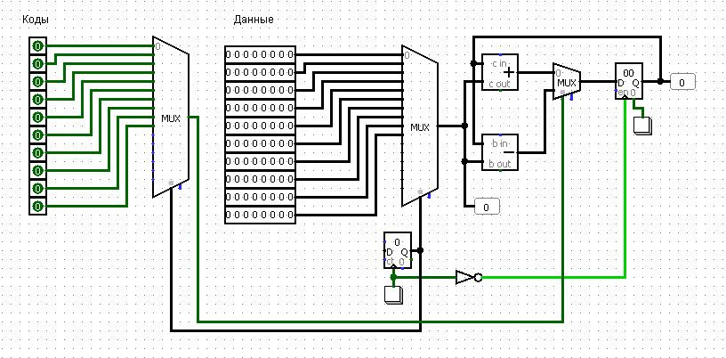
Next, let's say we need to find three sums: three terms, two terms, and two more terms. We implement a device that allows you to load a value from the memory into the battery and save the value from the battery to memory, for this we remove the Vychiyatel circuit, and the multiplexer that we used to select the operation will now be used to fetch data from the memory.
In order to implement the “save” command, in the “data” array, we replace the “Contact” elements with eight-bit registers; we will add a demultiplexer (decoder) for writing to registers.
Increase the width of the commands: command 10 loads the item from memory into the battery,
command 00 adds the number from memory to the battery, command 01 stores the value from the battery in memory. "Splitter" allows you to divide the bits of the command, send the low order to the multiplexer, the senior to the demultiplexer.

Replace individual registers with RAM arrays.
We will use a scheme with one synchronous read / write port (available by default). For the record we will use a managed buffer.
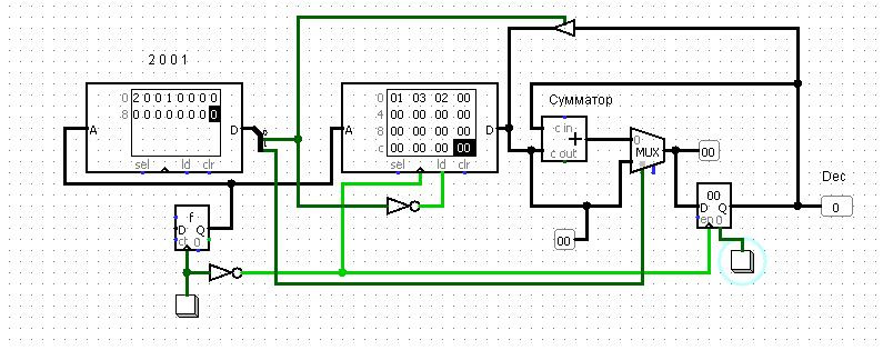
In our device, codes and data are stored in different memory blocks (Harvard architecture). We design a device in which codes and data will be stored in one block (von Neumann architecture).
In the first four digits of the eight-bit memory cell, the command will be stored; in the second four digits, the address (absolute direct addressing) will be stored.
We will load the address and command into separate registers, and then use the multiplexer to go to the saved address. To write data to RAM, we will use a pulse feed delay scheme based on a shift register.
Command 3 loads the item from memory to the battery, command 2 adds the number from memory to the battery, command 4 writes the contents of the battery to RAM.
Here is an example of a program that adds three numbers (cells 8, 9, a) and saves the result to a free cell (cell b): 38 29 2a 4b.
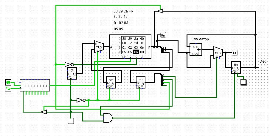
We also add the ability to make unconditional transitions.
We implement a device in which only one command will be executed - an unconditional branch command. To do this, we will send four low-order digits (the address itself) to the counter that generates the address, and we will send the command stored in the high-order digits of the memory cell to the download port.
For example, to jump to the cell with the address 6, the command 86 is used.

Add this device to the main circuit.
The resulting scheme allows you to add numbers (stored in memory), as well as jump to a cell with a specific address.

In general, there was already an article on geektimes devoted to designing a CPU in Logisim.
All schemes presented in the article can be downloaded in one file .
Logisim can be downloaded here.
Consider how the adder works on the example of the 155im3 chip (foreign analogue 7483). For the 155 series microcircuits, let's agree that there is an internal resistor at the inputs that pulls up to a plus (if the leg is “hanging in the air”, then there is a logical “one” on it), so when the power is connected to the microcircuit, all 5 LEDs connected to out.

This is the chip model in Logisim.

In order to design such a microcircuit in Logisim, it is necessary to select “Menu” - “Project” - “Add schema”.
Here is how this MS looks inside a subcircuit. These are four half- adders, combined into a full adder.

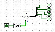
As the battery, we will use the 155TM8 (74175) microcircuit - quad D-flip-flop.
The triggers that are part of the MS pass through all the time while there is 1 at the synchronization input, not only along the front (triggers with static control), but in the Logisim program only triggers with dynamic control are available to us, but in this case it doesn’t matter ; we will use what is.
More about triggers can be found in Wikipedia.
We will assemble the MS 155tm8 model from D-flip-flops.
Further we will collect the scheme, allowing to put sets of numbers.
For example, if you add up a set of numbers 2 (0010), we get 2 (0010), 4 (0100), 6 (0110), etc.
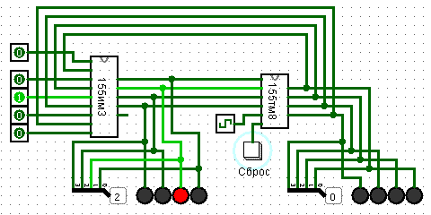
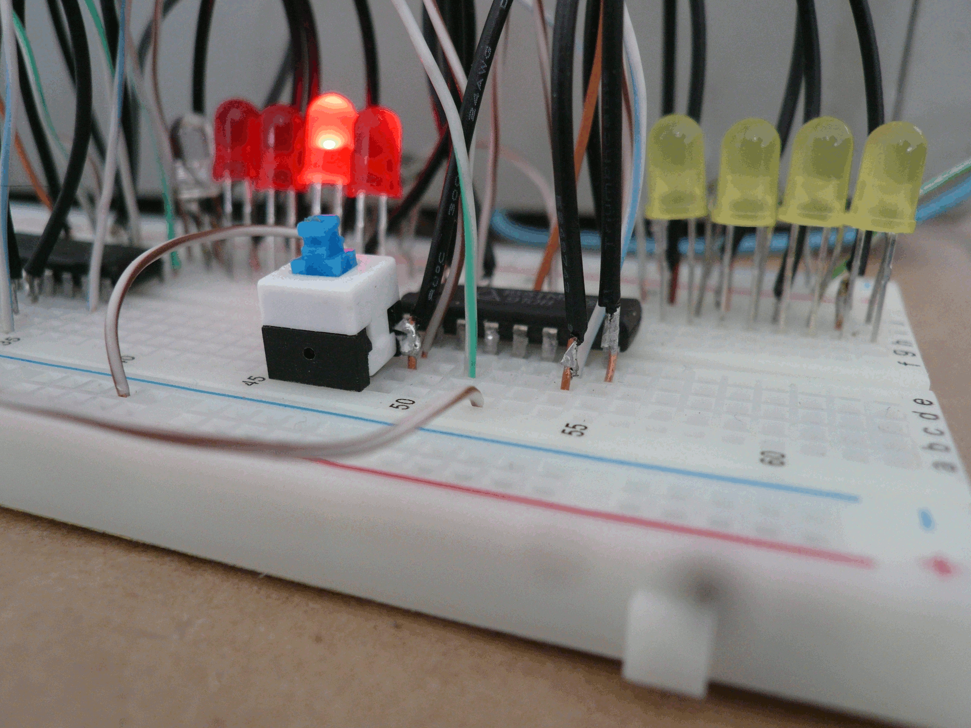
First, 2 appears at the output of the adder (red LEDs), then 2 is loaded into the quad D-Trigger (yellow LEDs), and 4 appears at the output of the adder, then 4 is loaded into 155m8, and 6 appears at the output of the adder.
In order to design a simple memory module (static), we need a multiplexer. Let's design the dual multiplexer 155kp2.

We also need a counter. We will design the chip 155e5.
This is a four-digit counter, but we only need two lower digits.
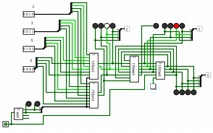
Let us store numbers, for example, 2 (0010), 3 (0011), 5 (0101).
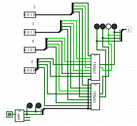

Let's unite all components in one scheme. We will add numbers that are stored in memory.
2 + 3 + 5.

Next, create a device that allows the operation "subtraction". In order to subtract a number, you must first translate it into a reverse code (replace all 0 with 1; all 1 with 0), and then into an additional code (add 1).
For storing numbers we will use 155ru2 (RAM), for translation into the reverse code we will use 155ln2 (six Elements Not). These chips have outputs with
open collector .
For MS 155ru2, we assume that the synchronization input and the recording resolution input are combined into one line. This (combined) input is static, the MS skips through all the time, while at the input there is 0 (low level).
Data enters the MS when a low level appears at this (combined) input, therefore we will hang the Element not to the clock input.
The outputs will be inverted, if connected according to the scheme I gave above for the output with OK (hang Elements Not to outputs), the chip select input is also inverted, the MS performs a write or read cycle only at the zero level on this input (hang Element Not to the input crystal selection).
Also, the MS has separate inputs for the address and for the data, so when choosing a standard RAM module (Side menu - Memory - RAM) on the “Data Interface” tab, you must select “Separate read and write ports”.
So The model closest to 155ru2 will be:
To select a number in the direct or inverse code, we will use a multiplexer. We will store the numbers 8, 4 (in the reverse code), 1.
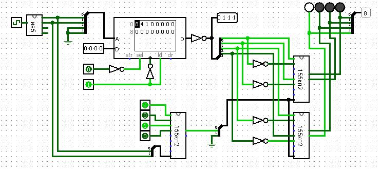

Let us combine our scheme with the previous one and subtract 4 from 8, i.e. 8 + 4 (in the return code) + 1.
So we have created the simplest programmable device in which teams select the number in the direct or reverse code.
Let's design our schemes on FPGA / FPGA. We will use Quartus II. The free version with limited functionality can be downloaded from the official site .
When registering in the My Primary Job Function is * section, select Student.
Next, you need to download the driver for the programmer (the driver for usb-blaster can be installed from C: \ altera \ ... \ quartus \ drivers \ usb-blaster).
In the Quartus environment, create a new project (“File” / “New” / “New Quartus II Project”) and add a Block Diagram / Schematic File (“File” / “New” / “Block Diagram / Schematic File”) to the project.
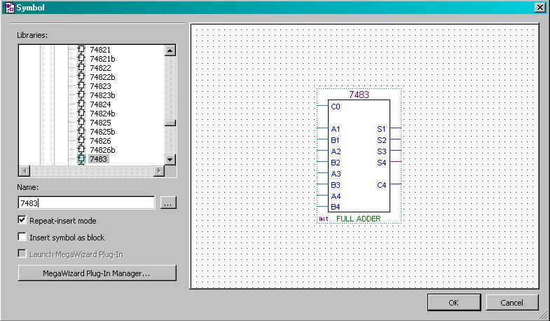
We will need an adder (7483) and a battery (74175).
These chips can be added from the Symbol Tool:

Adding I / O ports ("Symbol Tool" / "primitives" / "pin"), we get a scheme that allows you to add a set of four-digit numbers.

If you use an external clock source, the clock foot of the source must be pulled to the “ground”.
Schemes designed in Logisim can be downloaded in a single file .
Let's design a device in Logisim that allows you to sum up sets of numbers stored in memory. Let's take a set of eight-digit numbers and connect it to the multiplexer, transfer from one number to another will be done using a counter connected to the multiplexer select input, and connect the adder and the battery to the multiplexer output. We will use a button as a clock generator. Data will be loaded into the battery when the button is released (this is done using the NOT element connected to the button).
Next, we implement the operation “subtraction”, and we will store our operations (commands) in a hotel array. The “0” command performs addition, and the “1” commands - subtraction. Further, these commands are fed to the input of a multiplexer connected to the Adder and Subtractor.
')
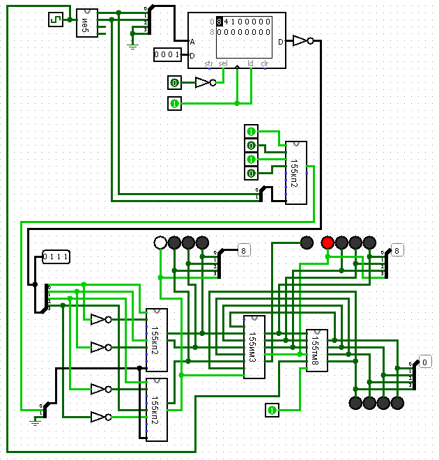
Next, let's say we need to find three sums: three terms, two terms, and two more terms. We implement a device that allows you to load a value from the memory into the battery and save the value from the battery to memory, for this we remove the Vychiyatel circuit, and the multiplexer that we used to select the operation will now be used to fetch data from the memory.
In order to implement the “save” command, in the “data” array, we replace the “Contact” elements with eight-bit registers; we will add a demultiplexer (decoder) for writing to registers.
Increase the width of the commands: command 10 loads the item from memory into the battery,
command 00 adds the number from memory to the battery, command 01 stores the value from the battery in memory. "Splitter" allows you to divide the bits of the command, send the low order to the multiplexer, the senior to the demultiplexer.
Replace individual registers with RAM arrays.
We will use a scheme with one synchronous read / write port (available by default). For the record we will use a managed buffer.
In our device, codes and data are stored in different memory blocks (Harvard architecture). We design a device in which codes and data will be stored in one block (von Neumann architecture).
In the first four digits of the eight-bit memory cell, the command will be stored; in the second four digits, the address (absolute direct addressing) will be stored.
We will load the address and command into separate registers, and then use the multiplexer to go to the saved address. To write data to RAM, we will use a pulse feed delay scheme based on a shift register.
Command 3 loads the item from memory to the battery, command 2 adds the number from memory to the battery, command 4 writes the contents of the battery to RAM.
Here is an example of a program that adds three numbers (cells 8, 9, a) and saves the result to a free cell (cell b): 38 29 2a 4b.
We also add the ability to make unconditional transitions.
We implement a device in which only one command will be executed - an unconditional branch command. To do this, we will send four low-order digits (the address itself) to the counter that generates the address, and we will send the command stored in the high-order digits of the memory cell to the download port.
For example, to jump to the cell with the address 6, the command 86 is used.
Add this device to the main circuit.
The resulting scheme allows you to add numbers (stored in memory), as well as jump to a cell with a specific address.
In general, there was already an article on geektimes devoted to designing a CPU in Logisim.
All schemes presented in the article can be downloaded in one file .
Logisim can be downloaded here.
Consider how the adder works on the example of the 155im3 chip (foreign analogue 7483). For the 155 series microcircuits, let's agree that there is an internal resistor at the inputs that pulls up to a plus (if the leg is “hanging in the air”, then there is a logical “one” on it), so when the power is connected to the microcircuit, all 5 LEDs connected to out.
This is the chip model in Logisim.
In order to design such a microcircuit in Logisim, it is necessary to select “Menu” - “Project” - “Add schema”.
Here is how this MS looks inside a subcircuit. These are four half- adders, combined into a full adder.
As the battery, we will use the 155TM8 (74175) microcircuit - quad D-flip-flop.
The triggers that are part of the MS pass through all the time while there is 1 at the synchronization input, not only along the front (triggers with static control), but in the Logisim program only triggers with dynamic control are available to us, but in this case it doesn’t matter ; we will use what is.
More about triggers can be found in Wikipedia.
We will assemble the MS 155tm8 model from D-flip-flops.
Further we will collect the scheme, allowing to put sets of numbers.
For example, if you add up a set of numbers 2 (0010), we get 2 (0010), 4 (0100), 6 (0110), etc.
First, 2 appears at the output of the adder (red LEDs), then 2 is loaded into the quad D-Trigger (yellow LEDs), and 4 appears at the output of the adder, then 4 is loaded into 155m8, and 6 appears at the output of the adder.
In order to design a simple memory module (static), we need a multiplexer. Let's design the dual multiplexer 155kp2.
We also need a counter. We will design the chip 155e5.
This is a four-digit counter, but we only need two lower digits.
Let us store numbers, for example, 2 (0010), 3 (0011), 5 (0101).
Let's unite all components in one scheme. We will add numbers that are stored in memory.
2 + 3 + 5.
Next, create a device that allows the operation "subtraction". In order to subtract a number, you must first translate it into a reverse code (replace all 0 with 1; all 1 with 0), and then into an additional code (add 1).
For storing numbers we will use 155ru2 (RAM), for translation into the reverse code we will use 155ln2 (six Elements Not). These chips have outputs with
open collector .
For MS 155ru2, we assume that the synchronization input and the recording resolution input are combined into one line. This (combined) input is static, the MS skips through all the time, while at the input there is 0 (low level).
Data enters the MS when a low level appears at this (combined) input, therefore we will hang the Element not to the clock input.
The outputs will be inverted, if connected according to the scheme I gave above for the output with OK (hang Elements Not to outputs), the chip select input is also inverted, the MS performs a write or read cycle only at the zero level on this input (hang Element Not to the input crystal selection).
Also, the MS has separate inputs for the address and for the data, so when choosing a standard RAM module (Side menu - Memory - RAM) on the “Data Interface” tab, you must select “Separate read and write ports”.
So The model closest to 155ru2 will be:
To select a number in the direct or inverse code, we will use a multiplexer. We will store the numbers 8, 4 (in the reverse code), 1.
Let us combine our scheme with the previous one and subtract 4 from 8, i.e. 8 + 4 (in the return code) + 1.
So we have created the simplest programmable device in which teams select the number in the direct or reverse code.
Let's design our schemes on FPGA / FPGA. We will use Quartus II. The free version with limited functionality can be downloaded from the official site .
When registering in the My Primary Job Function is * section, select Student.
Next, you need to download the driver for the programmer (the driver for usb-blaster can be installed from C: \ altera \ ... \ quartus \ drivers \ usb-blaster).
In the Quartus environment, create a new project (“File” / “New” / “New Quartus II Project”) and add a Block Diagram / Schematic File (“File” / “New” / “Block Diagram / Schematic File”) to the project.
We will need an adder (7483) and a battery (74175).
These chips can be added from the Symbol Tool:
Adding I / O ports ("Symbol Tool" / "primitives" / "pin"), we get a scheme that allows you to add a set of four-digit numbers.
If you use an external clock source, the clock foot of the source must be pulled to the “ground”.
Schemes designed in Logisim can be downloaded in a single file .
Source: https://habr.com/ru/post/354978/
All Articles